SSR or Solid state relays are high power electrical switches that work without involving mechanical contacts, instead they use just a couple of solid state semiconductors like MOSFETs for switching an electrical load, smoothly, and with high efficiency.
SSRs can be used for operating high power loads, through a small input trigger voltage with negligible current.
These devices can be used for operating high power AC loads as well as DC loads.
Solid State Relays are highly efficient compared to the electro-mechanical relays due to a few distinct features.
Main Features and Advantages of SSR
The main features and advantages of solid state relays or SSRs are:
- SSRs can be built easily using a minimum number ordinary electronic parts
- They work without any form of clicking sound due to the absence of mechanical contacts.
- Being solid state also means SSRs can switch at much faster speed than the traditional electro-mechanical types.
- SSRs do not depend external supply for switching ON, rather extract the supply from the load itself.
- They work using negligible current and therefore do not drain battery in battery operated systems. This also ensures negligible idle current for the device.
Basic SSR Working Concept using MOSFETs
In one of my earlier posts I explained how a MOSFET based bidirectional switch could be used for operating any desired electrical load, just like a standard mechanical switch , but with exceptional advantages.
The same MOSFET bidirectional switch concept could be applied for making an ideal SSR device.
For a Triac based SSR please refer to this post
Basic SSR Design
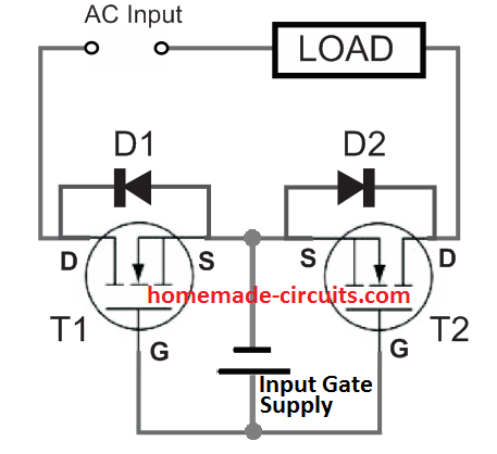
In the above shown basic SSR design, we can see a couple of appropriately rated MOSFETs T1 and T2 connected back to back with their source and gate terminals joined in common with each other.
D1 and D2 are internal body diodes across the drain/source of the respective MOSFETs.
An input DC supply can also be seen attached across the common gate/source terminals of the two MOSFETs. This supply is used for triggering the MOSFETs ON or for enabling permanent switch ON for the MOSFETs while the SSR unit is operational.
The AC supply which could be up to grid mains level and the load are connected in series across the two drains of the MOSFETs.
How it Works
The working of the proposed sold state relay can be understood by referring to the following diagram, and the corresponding details:
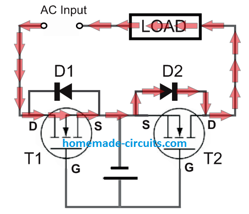
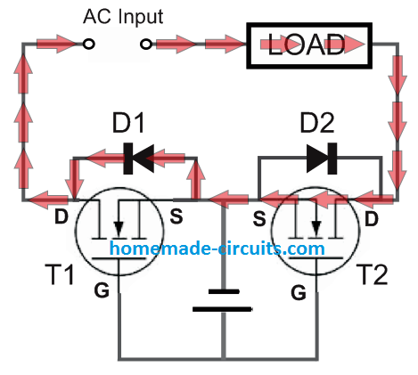
With the above setup, due to the input gate supply connected, T1 and T2 are both in the switched ON position.
When the load side AC input is switched ON, then both T1 and T2 are already turned ON by the gate supply. Since a MOSFET channel can conduct current in either direction when the MOSFET is ON, the AC current flows through the low-resistance channels of both MOSFETs during both half cycles.
During the positive half cycle, current flows through the channel of T1 and then through the channel of T2 in the opposite direction. During the negative half cycle, the current reverses direction but both MOSFET channels continue to provide the conduction path.
Although each MOSFET has an internal body diode, these diodes do not normally carry the load current when the MOSFETs are ON.
The ON-resistance of the MOSFET channels is very low so the voltage drop across the channels is much lower than the forward voltage of the body diodes, which causes the body diodes to carry negligible current.
When the gate supply is removed and both MOSFETs turn OFF, then their channels stop conducting. At this point, the two body diodes are connected in opposite directions, so they block current in both directions. This allows the back-to-back MOSFET arrangement to switch and block the AC load in both directions.
Here's an excerpt from the datasheet of the article.

Video showing the testing of the above SSR circuit
Making a Practical SSR Circuit
Why We Use Two MOSFETs For AC
When we want to switch AC using MOSFETs then we find that a single MOSFET cannot block current in both directions because of its body diode.
So we use two N Channel MOSFETs and we connect their sources together and we keep their drains toward the AC line terminals.
When we do this arrangement then the body diodes oppose each other and the AC can be fully blocked when the gate drive is zero. So the pair works like an AC switch.
Why We Need A Floating 15 V Supply
When we use back to back MOSFETs in AC circuits then the common source point does not stay at ground level.
This point keeps moving up and down with the AC waveform, so now we understand that the gate voltage also must follow this moving point, because the MOSFET only cares about the Vgs difference.
When the source rises, then gate must rise above it, when the source falls, then gate must fall above it.
So we need an isolated 15 V supply that floats along with the MOSFET sources.
When the supply is floating, then it does not care about earth or neutral and it simply rides with the circuit, so the MOSFET always sees a correct gate voltage.
Why The Source Node And The 15 V Negative Can Touch
Many people think that isolation is broken when the isolated supply negative is connected to the MOSFET source node.
But since the isolated supply has no link with mains or earth, it does not matter. It only follows the MOSFETs.
So the 0 V of the 15 V supply becomes the reference for the MOSFET gates and sources.
When we do this connection, everything still stays isolated from the outside world.
How The Gate Is Driven From The 12 V Control Side
We use an opto or a small control section in the 12 V side. When we give 12 V input to this module then the opto transistor pulls the floating 15 V supply positive toward the MOSFET gate through the gate resistor.
When this happens then the MOSFETs get a Vgs of around 12 V and they turn ON.
When we remove the 12 V input then the gate is left without drive and the resistor that we added slowly discharges the gate. When the gate reaches the same level as the source then the MOSFETs turn OFF.
How The Circuit Behaves When AC Passes
When the AC line is connected to the MOSFET drains then common source node becomes a floating midpoint that shifts according to the load and the waveform.
But the gate supply also floats in the same way so the Vgs stays correct.
When we give the 12 V command, then MOSFETs turn ON in both half cycles and the AC flows without restriction.
When the input is removed then the gate falls down through the 1 M resistor and the MOSFETs turn OFF and block both directions due to the anti series body diode configuration.
Why 220k Is Acceptable In This SSR
We use 220k because we do not need ultra fast gate discharge, and because the SSR is not switching at very high speed.
The AC cycle itself is very slow compared to MOSFET switching, so even a 10 ms or 20 ms fall time is perfectly OK. The 220k value also keeps the loading of the 15 V supply to a very small level, but if you want a little faster discharge you can use 100 K also. Both values work fine because the switching is slow.
Final View Of The Completed SSR
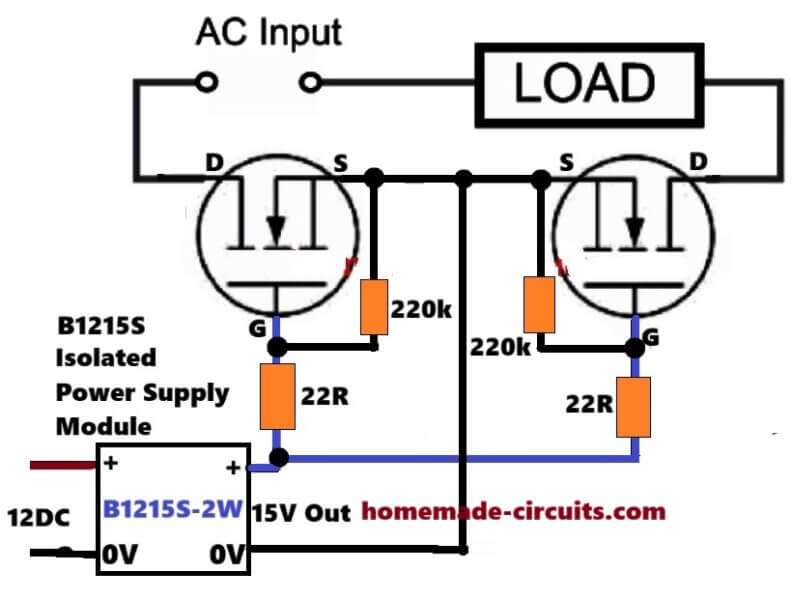
So now the whole SSR becomes very simple. Two N Channel MOSFETs are connected source to source, the drains go to AC.
The floating 15 V positive is fed to the gates through individual 22 Ohms.
The floating 15 V negative goes to the common source.
A 220 K resistor is placed between the gates and the sources of each of the MOSFETs.
The isolated 12 V side drives the opto, and the opto connects the 15 V positive to the gate when it receives the command.
Conclusion
So now we get a simple, very easy to understand bidirectional MOSFET SSR which can switch AC efficiently.
The use of the floating 15 V module makes the design work smoothly even when the AC line moves up and down.
The resistors keeps the gate under control.
Source.
Reference: SSR



Questions & Answers
Hello sir swagatam,help me understand;
1. 100k and zener act as voltage divider/step down?
2. I understand that during the positive half cycle,power goes through D1,100k zener and D3 back to load, so my question is, Can 12v zener diode and 100k hold a huge load say 5000w load ac?
3. Can I this idea be used to switch more than 200A DC? How?
4. Can this circuit be used as a 12v step down for inverter change over? Also how?
Evans, the 100k and the zener are for biasing the MOSFET gates, the load is switched through the MOSFETs and the internal body diodes and therefore can be dimensioned for switching any desired load.
Understood sir swagatam,I think was missing a point but got it. Now please correct me if I’m wrong, is it true that the load will be powered by dc since power goes through the mosfets internal body diode? If so , isn’t there any way this can be made to pass ac to the load?
The devices will conduct alternately for switching the AC input, please see the arrow diagram
Sir swagatam,any diagram with p channel mosfets?
pchannel is not recommended due to its higher resistance compared to N channel
Thanks you for publishing this, however I must make one very important point:
When dealing with the AC Grid mains, you must provide some sort of isolation between the low voltage trigger input and the mains. Maybe an opto-isolator or a reed switch?
Also, what is the purpose of the second circuit (with the 12 volt DC power supply?) How do the mosfets get triggered to control the AC load?
Note, that circuit requires isolation for the low voltage DC as well.
Thanks
Thank you, the SSR explained above is designed to derive the gate voltage from the load itself, not from any external source, therefore isolation is not necessary. Moreover the entire configuration is supposed to be enclosed inside a sealed module. Also the Opto coupler would require more current than a 100k resistor so that may not be appropriate for an SSR design.
The first two designs are for explaining the concept and the conduction path of the module. The battery sign at the mosfet gate shows a biasing DC input for the gate.
I am sorry…Yes an opto coupler should be added for an external low current switching, in my earlier diagram I completely missed that if the gates were connected with the 100K/zener output that would keep the SSR permanently ON. I have changed the design now for your reference.
Is this system suitable for powering inductive loads? The reason why I am asking this is because,power is rectified to DC before reaching the load.
All types of AC load can be powered, please see the arrow diagram.
I can see the arrows show that power passes through the forward biased diodes in either cycles,this will in turn be rectified to DC. Am I right or wrong?
The DC is rectified and used for the gates, not for the load. The load will be switched with the input AC only.
If I connect the gates directly without a switch,is there any issues?
The MOSFETs and the load will be permanently switched ON then.
Sir can you give a system for a full bridge topology using 4 N channel mosfets?
Swagatam: Thanks mate. In my 50+ years of work in the IT industry I have been taught many a lesson by the old “240”. Many faulty power switches, many incorrectly wired extension cables, many mistakes by unknown “dodgy” sparkies. I am still here, but I wonder if the fibulation I suffer from can be attributed to those “shocking” events…
Jeff
That’s awesome mate, I appreciate your knowledge and help! Please keep up the good work!
Hello Sir,
I have a question about this project. I like this project and may use it. However I would like to use something like this that would take the place of a standard SPDT relay for DC. Basically to replace the relays in one of your other circuits used to charge two 2 batteries flip-flop style. Thank you much for all you do.
Hello Joel, for a SPDT DC version you can probably try this concept:
https://www.homemade-circuits.com/12v-dc-solid-state-relay-ssr-100-amps/
Thank you I found it and it looks like it will fit just the way I wanted. I enjoy your site and play with your circuits to draw pc boards with. Just for fun.
Glad you are enjoying my site, please keep up the good work!
I have a question about the circuit that you directed me to. I have used your split 12v charger and the above mosfet circuit you directed me to, for a project I want to build. My question is by looking at what you showed me it seems that the mosfets switch the ground and not the positive side? If that is true the common is nothing more than the positive side of the battery? Y or N. Have not done much work with mosfets which is why I ask.
Thanks much for your help.
yes, that’s correct, even in a relay you have one of the load terminals connected to + or the – line.
Ok I thought so just wanted to make sure I was seeing things right. Thanks again
This is exactly what I want. However I need to switch AC on/off by means of 12v dc. If I connect +12v to the combined gates I don’t think it will work, will it? So how do I do this please?
It will work if you connect the the 12V DC across the gates and the sources of the MOSFETs as indicated in the first diagram.
You mean -12 connected to 240ac? Also if the gates are left floating will it switch of?
Tks for your help
yes that’s right….
gates must not be kept open…
I disconnected +12v from gates and have a 10k resistor between gates & sources but it’s still on,
so how do I switch it off?
Can be difficult to judge without seeing your circuit practically??
Hello, great tutorial, but I had a question. Since half of the time, the one mosfet has current going through its body diode which often has a voltage drop of 1-2V in the models I’ve seen, wouldn’t the mosfets get very hot for higher loads? Or do they not because they are only in this state half of the time? Thanks.
Hi, to ensure an efficient working you will have to complement the mosfets with more number if parallel mosfets
Nice article, how would you drive this from an Arduino if the load is 400 watts?
Then a totem pole would be needed to drive T1 & T2?
Glad you liked it, I think the last concept would be suitable for interfacing with an arduino
Hey Swagatam,
i am wondering how your rectifier can supply the Zener after the SSR has been switched on.
Imagine we are in the positive Half of the Sinewave.
If one of the Mosfets is swicthed on (lets say T1) then D3 of T2 is also in conducting mode. So lets say over T1 is 0.3V and over D3 is 0.7V then you have 0.3V+0.7V=1V for your Zener diode (after rectifier Diodes…), which tries to hold the OnState of the SSR. So, please correct me, but this will not work.
Best regards Tim
Hi Tim, During the half cycle before T1 can conduct the capacitor will be charged and this will hold the supply across the zener diode and also for the MOSFET gates.
Here’s the original link from where I referred the concepts:
https://www.ti.com/lit/ug/tiduc87a/tiduc87a.pdf
Thanks for your answer. Please have a look at page 12; “2.4 Undervoltage Lockout Design Theory”.
The cap will discharge as long as the SSR is in switched on and after some time it must be switched off to reload the cap again. So this is a good solution for something, that is switched on only for a short time, like a thermostat or something. The Texas guys seem to switch it at a certain point off and on again, so the cap reloads. Well its not a problem, but one have to know it before.
Dear Swatagam
I love your site and its amaze me everytime thank you for opening site like this
Can you give a specific value of diodes?
Dc out? How much voltage needed for circuit first stage(capacitors,resistor,part)?
You say for fast switching add opto coupler so triggering opto coupler need another voltage input?
Thank you for your patience and answering <3
Thank you Trishpota, The diode rating will be twice of the load current rating. If load is 2 amp, then diodes must be 4 amps. Only 12V to 17 V DC will be enough for the MOSFET switching. Yes the opto will need to be switched externally from an external trigger source, because in an SSR the input and output is supposed to be completely isolated.
What about zener diode?
zener diode is 15 V, please make the last circuit which will ensure correct working of the SSR. Once confirmed you can break the red line and introduce an opto based switching through that line.
Hi Swagatam,
I have few doubts referring to the figure 2 of current flow.
1) since both the mosfets are turned on at a time the current should flow from both the mosfets rather than the diode, though the current only flows from the drain to source and not from the S to D, it taken a path from the diode please correct me if I’m wrong.
2) when the gate is powered or triggered with the DC supply voltage and the positive half cycle AC signal is passed from the mosfet, since the negative terminal of the DC supply is connected to the common source then why the positive half AC signal did not taken that DC supply ground path rather than flowing through the diode.
please let me know the above doubts I’m new to the electronic design thanks.
Hi Steven,
1) the current will take the easiest path which is through the forward biased diode, and therefore the associated MOSFET will remains completely ignored and turned OFF
2) Referring to the first diagram, the opposite pole of the AC is across its own supply points not the DC negative, so it will flow towards its own negative/positive points not the external DC negative. The points indicated as “AC Input” are referenced with each other, not to an external DC
Hi !
What is AC load?
Any appliance…
Hi friend! I really enjoyed the class, it was magnificent; his way of narrating is that of a great Professor.
I would like, if it were possible a tip on how to create a circuit to keep the soldering iron of 30w, with an ideal temperature, constant. Thank you for the class and Congratulations!
Thank you friend, you can use the second circuit explained in the following post:
https://www.homemade-circuits.com/fan-speed-controller-for-heatsink/