In this post we'll study a simple high current mosfet based SPDT DC relay, which can be used in place conventional bulky SPDT mechanical relays. The idea was requested by Mr. Abu-Hafss.
Working Concept
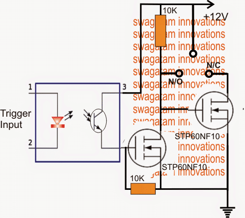
A simple high current SPDT solid state DC relay or a DC SSR can be constructed using a couple of mosfets and an optocoupler, as shown in the digaram above.
The idea looks self explanatory.
In an absence of an external trigger, the lower mosfet stays switched OFF allowing the upper mosfet to conduct through the 10k resistor connected across the positive and the gate of the mosfet.
This enables the N/C contact to get active, and a DC load connected across the supply positive and the N/C gets activated in this situation and vice versa.
Conversely in the presence of an input trigger, the mosfet connected with the opto emitter gets an opportunity to switch ON, switching OFF the upper mosfet.
In this situation a load connected between positive and N/O points gets activated or vice versa.
The Circuit Diagram
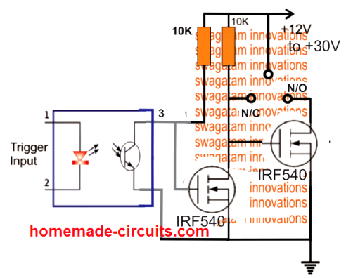
The above design can be configured in the following manner, and in fact this appears to be technically more correct, and therefore is the recommended one.
This design will work regardless of the opto input switching voltage, right from 3V to 30V DC.
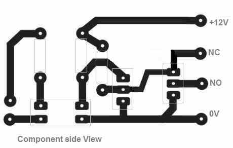
PCB Layout
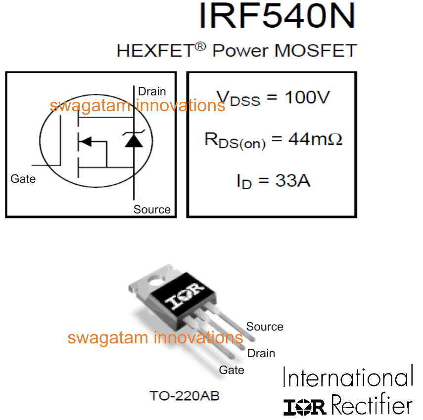
The following image shows the pinout details of the MOSFET IRF540, you can use any other MOSFET of your choice and as desired:
Upgrading the SPDT Relay to DPDT Version
Creating a DPDT version of the above DC solid state relay is actually not too difficult. We can do this by adding a couple of more MOSFETs as shown in the following illustration.
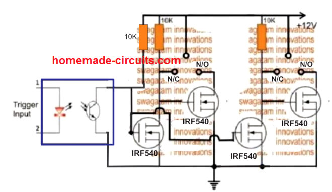
Here, although the poles appear to be a single pole, connected with the positive line, it could be simply separated and integrated with the different DC supplies for operating two individual loads, and implementing a DPDT SSR function.


Comments (122)
Hi Swagatam,
Firstly, elegant design and wonderful to see someone so willing to help. I am only just beginning to learn about semiconductors, most of my electrical knowledge is based on 12vdc automotive applications this is what has lead me to your design. I am looking to create a NC SPDT SSR. This is to be triggered by a 12vdc source. My aim is to be able to interrupt a low output (earth) from the ecu that is used to activate an ignition coil.
In this application the coil is supplied +12v from the ignition and the ecu supply’s the -12v.
Using conventional SPDT relay or “switching relay” I would wire the output from the ECU to the COM terminal, then connect the negative side of the coil to the NC terminal, and no connection to the NO terminal. This would allow the ECU signal to trigger the ignition coil until the relay is activated creating an open circuit. Is it possible to utilise your design in this application?
Regards
Haydn
Thank you Haydn, for your interesting question!
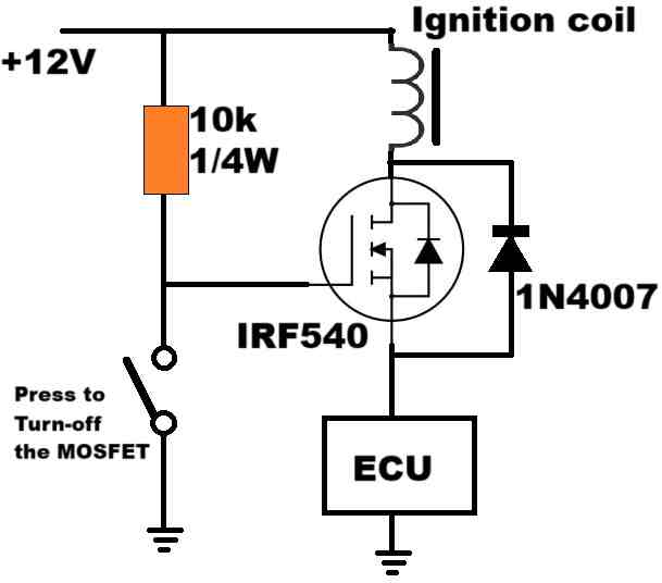
If I understood your requirement correctly, the following design should do the job for you.:
If it doesn’t, please let me know, then I may have to replace the N-channel MOSET with a P-Channel MOSFET.
Let me know if it works or not?
Merci d’avoir répondu rapidement, j’ai bien compris pour le circuit que je dois faire.
Merci infiniment
Laurent
You are welcome Laurent!!
Hello there,this is my first time visiting here. I want to ask:
By using the schematic above, will there be a delay (in ms) when switching from NO to NC and vice versa, or the transition can occur instantly?
There may be a negligible delay in microseconds which may be practically undetectable.
Great circuit. What if I wanted to switch 12VDC to control a circuit instead of ground. Most SSR’s switch voltage source to control a device instead of ground.
Glad you liked the post. For sourcing +12V the N-channel MOSFET side configuration will need to be replaced with P-channel MOSFETs. It’s as simple as that.
Thanks, Swagatam!
My pleasure Greg!!
Hi Swagatam, I’m trying to build a more generic relay replacement where the common output could be positive, negative or signal of some kind that can either be opened from normally closed or applied through normally open. I may want to wire them up reversal rest at ground for actuators or use them for hi low series parallel switching. This design seem to hold common at 12V I need all contacts isolated like a mechanical relay where they don’t switch power but take whatever is on the common contact and either connects or disconnects it through normaly open or normaly closed. Is this possible with mosfet or should I be using something else?
Hi Robert,
Presently I can’t figure out how this can be done. This can be probably created using a couple of mosfets, like in half-bridge driver circuit, but designing the configuration seems a little confusing right now. It will need some deep thinking.
Hi,
Wondering how we can adapt the SPDT circuit so that we can switch a signal between two outputs? I am not trying to switch power between two loads, but am trying to steer a signal one of two paths. Not sure how to make sure N/C is properly isolated without a conducting path when we apply a signal to the optocoupler and move the switch to N/O.
Hi, in an SPDT switch the contacts are perfectly isolated and the signals will never short across each other while toggling the switch.
You can connect the signal input to the center pin of the switch and connect the two outputs to the two outer pins of the switch.
Hello Swagatam,
Thank you for showing me how to assemble the transistors on the new PCB you designed. You have been very patient with me and have done so much in helping me that the work that is ahead of me will be so much easier! I have also learned some things from you that I didn’t know until I made contact with you and for all you have done I am forever grateful. I will update you when I start using the new PCB and relay you designed with my water level indicator.
Have a GREAT New Year!
Rudy
You are most welcome Rudy, Let me know if you have any further doubts or problems with any of the circuits.
I wish you too a Great New Year.
Hello Swagatam,
I just wanted to give you an update on the new PCB relay design you made for me. I just soldered all the parts on the board and tested it with my water level indicator circuit and it worked perfectly.
I am so grateful to you for the help you provided for me to have designed a solid state relay in place of the mechanical relay I have been using. I had been asking in other forums and no one ever gave me an answer to my problem, UNTIL I landed on your web page!
A couple of my family members have been asking me if it’s possible to have a circuit designed that could send the LED water level indicating to a smart phone or a computer so I told them I would ask you since you have the knowledge and are up to date on issues like this. If it’s possible, that would be so convenient and simple for anyone wanting to know how much water is in their tank, especially the elderly people I am helping in trying to make their lives better.
Now that I have tested your new PCB relay I am going to try to design your relay and my level indicator and combine them together into one PCB. I will update you on my progress.
Thank You AGAIN!
Rudy
Thank you Rudy, it’s my pleasure!
I am so glad you could make and implement the relay control operations successfully.
However, regarding the cellphone based transmission, it is beyond my reach, since the idea will require complex microcontroller coding and creating a cellphone Application.
All the best to you, let me know if you have any further problems with the circuit.
Hello Swagatam,
I want to explain more clearly how the siren is to function in my application.
When the water level in the tank is in contact with the probe where I get the +9V the siren is supposed to be off. When the water level drops down below the probe that is when the siren alarm should go off.
The siren is to let me know that we are out of water.
I built the ckt. with the P2N222 transistor and hooked it up to the probe but the siren turns on as soon as the water level makes contact with the probe but I want the siren to turn on when the water is not in contact with the probe.
The main reason I was originally using the relay was to get the result that I wanted in turning on the siren when out of water. I decided to use your MOSFET relay because it was a lot better and more reliable than the mecanical relay that I was using and might use less current to keep it energized and might help the
12 V battery last longer without discharging sooner. Also I was not sure if the relay I was using would last long because the coil was always energized as long as the probe touched the water and since I had never used that relay I wasn’t too comfortable using it.
Hope this helps you to see what I need for my application.
Thank you AGAIN!!
No problem Rudy,
In that case you can try the following PCB design:
Here I have removed the opto coupler. Since the input and output DCs are of the same level, an opto isolation is not required.
I have replaced the input transistor with a BC547
For the output transistor you can use an IRF540 or TIP31.
Hope it works.
Swagatam, I saw the new design with the new PCB with the new transistor but I don’t know how to identify the pins and how to mount them to the new PCB.
Have you made a schematic of this new PCB? It would be helpful in helping me identify where the parts go and also help me to add it to my water level indicator circuit that I am using now.
I continue to being grateful and thankful for all you have done for me. You have helped me resolve some issues that I couldn’t have done without you!
Hello Rudy, I am always happy to help, so no problems at all.
The transistor pinouts can be easily identified.
Assuming you are using BC547 for T1, and TIP31 for T2, then you just have to insert the emitter pin of the transistors into the pads that are associated with ground line. Once you do this the other two pins will automatically fall into place. Meaning, once you insert the emitters to the ground line pads, the base the collector pins will automatically go into their remaining two pads respectively.
If you are using an IRF540 for T2, then again, you can simply insert the SOURCE pin of the mosfet into the ground pad, and the remaining pins will automatically go into their appropriate pads.
However, I am sorry it will be difficult for me to add this design into your PCB because I have not fully studied your water level controller design.
As you explained in your previous email, that when the water is available across the input probes, the siren must remain switched OFF, and it must sound whenever there’s no water available across the probes….so this circuit will fulfill this perfectly.
I have shown 12V as the input trigger instead of 9V, because 12V is already being used for switching the siren, so the same 12V can be also used as the triggering voltage through the water.
hope this image is better photos.app.goo.gl/29MrFC192NGbJEo67
Thanks for showing me how to correct the PCB.
I will update you after I make the changes.
You mentioned that I could use other MOSFET. Do you have the name, number of some others that I could buy?
By the way, I am using a 360 ohm current limiting resistor for the PC817 opto coupler. I have 9 volts before the resistor going pin 1 of the PC817. Is this correct?
THANKS AGAIN!!
Sure, no problem.
360 ohm will be fine according to me.
The mosfet specs will depend on the load specs. If you can tell me about the voltage and current specifications of the load, then I can try to figure out the alternate mosfet numbers.
Hello Swagatam,
Thanks again for the new PCB design. I will be wiring up the corrected design just after Christmas.
I bought the PCB Wizard software program so that I could try learning how to do more schematics for the circuits that I am using for my water level indicator and maybe improve on what I am doing now.
I have designed a schematic that I have completed with the new program that includes your design of the MOSFET Relay and my design of the water level indicator and I was wondering if you would do me a favor and check it out if you have some time to see if it will work as designed. I could send it to you if you are interested in doing this for me. If you are, I am not sure if I could just paste it to here or if there is another way to send it to you so you could see it.
I hope I am not asking too much from you, I just don’t know where else to go to do this and I an truly grateful for all the help you have been to me thus far!
Thank you
You are welcome Rudy,
if your design is not too large and if it is send to me in a schematic format then I can probably can have a look at it and try to solve it for you.
You can upload your schematic to any free online image hosting site and provide me the link here through comment. Please make sure to remove the https from the link so that the comment does not disappear into the spam folder.
Hello Swagatam,
This is the link for the schematic. Hope this works.
photos.app.goo.gl/hnBQaiLcVpiJkqdz5
Hi Rudy, it looks OK to me and matching with my PCB layout, however if the load is a single load then two transistors may not be required, it can be simply handled by a single mosfet.
Thank you again for checking out the schematic!
I am glad that there were no mistake on the schematic I drew up.
I only have the siren that I need to turn on or off in my water level indicator and siren alarm but i didn’t know that I could control this with just 1 MOSFET. Could you please correct my schematic and show me how to use only 1 MOSFET to control the alarm? I would appreciate all the help you have given me thus far and anything more you could do for me.
Is there any way that I could compensate you for all you have done for me?
Actually you won’t even require a MOSFET and an opto-coupler, you will just require a BJT switching stage as shown in the following PCB design. You can easily accommodate it in your main PCB layout as per your convenience. Compensation is not required, I am happy to help without any compensation.
Hello Swagatam,
I wanted to know if a PCB has ever been designed for the SPDT solid state relay using the 2 IRF540 as you designed it in this article. (Image #2)
I can really use this relay for the water level indicator I make but I need a pcb module for what I am making.
The other question I have is do you know anyone that could design the gerber file so that I could have someone make the PCB of your design for me.
I am using a 12 VDC 10 amp 250 Vac relay module just now (JQC-3FF-S-Z) but would prefer to use your design instead.
I do no have a lot of knowledge in electronics but the 9-12 VDC water level indicator is very simple and I am making it and installing the system for many of my neighbors and friends. We all live in an area where we have the have our water delivered and has to be stored in water storage tanks.
The system I am building is helping many of my neighbors now and a PCB for your relay would help me tremendously in putting the system together and save me a lot of time in the assembling the parts together. I am an 81 year old guy trying to help some of the people in this area and not having to run out of water so often.
I would appreciate any help you might be able to give me.
Thank you for all the good you are doing in helping so many people with their projects.
Rudy
Thank you Rudy, I appreciate your interest and your efforts to help your neighbors.
However, unfortunately there’s no ready PCB design for the above concept.
Nevertheless, I can try creating a PCB layout design for the second schematic, without gerber files, if this fulfills your requirement.
Thank you so much for your prompt response. I would really appreciate it if you did that for me. This will help me in the assembly of my parts.
Do you have any suggestions on how and where I can get the gerbil file done and where to get the pin made?
I am truly grateful for your help!!
Have a blessed day
I have uploaded the PCB designs for the second schematic, you can check it out.
The PCB size will need to be scaled down appropriately by comparing with real component lead dimensions.
First of all, I want to thank you for helping me with designing the PCB. You have been a great help for me! The PCB looks great!
I am not clear about the opto coupler how it is hooked up to the relay and exactly where it is mounted on the PCB. How do I determine the value of the resister for the coupler.
Lastly, Is the coupler necessary and what is the purpose for it. I mentioned that I am not very knowledgeable on electronics so I am just trying to understand the circuit.
Have a good day!
Thank you, I am always glad to help!
The opto coupler can be seen at the bottom left of the PCB. I have shown a 4 pin opto coupler such as the PC817.
The opto LED resistor can be typically determined using the following formula:
R = LED supply Voltage – LED forward voltage / Max LED current
The opto coupler ensures that the input trigger DC is well isolated from the output load switching voltage.
If the difference between input and output voltage is not too high then the opto coupler can be avoided, and the input trigger voltage to the mosfet gate can be extracted from the load voltage itself.
Hi Swagatam, Thank you for designing the PCB for me. I copied the design and made the PCB exactly as the design you made. The PCb came out very good and a mirror solder side of the board looks exactly like your design.
I mounted all the components on the board as shown on the schematic and it doesn’t work.
I made sure all the components were soldered correctly and were hooked up correctly and I noticed that the #2 schematic has the NO hooked up to the drain of Q1 but the PCB design has it wired to the gate. Could this be the reason that the relay doesn’t work? Since I am not that knowledgeable on electronics, I couldn’t figure out what to do. I am sure that all the components are wired in the correct place as per the PCB design.
I have been encouraged about what I am trying to accomplish as the result of all the help you have given me. If there were more people like you the world would be a better place!
Thank You
Thank you again for all your help.
Thank you Rudy, for trying the PCB.
Yes there seems to be a small mistake in the PCB design, I have corrected it now, and have updated the new design.
But you don’t have to change your existing PCB, you can simply do some minor corrections on it, like cutting one of the tracks with a sharp knife, and joining a couple of points with a jumper wire.
Here’s what exactly you need to do with your existing PCB:
No problem at all. I will try to do it soon, and let you once it is posted.
Regarding gerber files I have no idea from where this can be done, so I am unable to suggest much on this!
First, You are an extraordinary person. Aside from your engineering knowledge, you are patient and strive to help others. I read all 80 comments and consistently you were supportive. We are exceptionally lucky you are so generous.
My search for help:
I am building an electric door strike control circuit. Fundamentally the circuit consists of a momentary capacitive switch which triggers a timer which energizes the solenoid of the electric door strike. Energizing the door strike enables the door to be opened. I dont need help with that part of the design.
I do need help with the Schurter 3-101-404
Capacitive switch regarding two issues:
The switch provides me with access to three internal leds each connected to an internal 3.3 bus where the 3.3 vdc come from in internal power supply powered by an external supply
Ranging from 5-28 vdc
My understanding of the spec sheet is that i only need to ground the other side of each led to turn it on. Not sure why a current limiting resistor does not exist between the led and ground. Regardless i want to operate these leds with a SPDT circuit. I would like to use
Your design but do not know enough to
Grasp if i can replace your 12vdc supply
With the 3vdc supply internal to the capacitive
Switch. Will the FETs still work at that low 3.3 vdc voltage?
The operation of the leds is such that one led is always on regardless of door strike state.
I intend to turn on the red led when the door strike is NOT energized. When the door strike IS energized i intend that the red light is turned off and the green light is turned on as long as the door strike is energized. When the door strike is no longer energized, the green led is turned off and the red led turned on.Hence the SPDT design.
Because one of the leds is always on
I am hoping the capacitive switch internal 3.3 vdc source seen through a led can be used as the Bus driving the FETs of your design.
Second issue:
My power supply for this project is a Mean well
Irm-30-24st. It is a floating 24 dc supply
The capacitive switch, on the other hand, is intended to be driven by a grounded supply
Whose voltage ranges from 5-28 vdc and can switch a max of 60Vdc and a current of 100 ma. Can i use the floating feature of my supply connecting the -12 vdc to the switch’s ground and +12 vdc to the switch Vin?
How will the switch’s internal power supply generate the 3 vdc to supply the leds?
In my mind, the 3 vdc coukd be generated by
The difference of any set of Voltages within the supply range. Hence if my -12vdc is attached at the switch ground lug, the 3 vdc led bus will actually be -9 vdc relative to the -12vdc. Is this true?
Yes, i could ground one side of my power supply and avoid the question. But that question bothers me. I need to understand
The case of the floating power supply vs grounded supply.
Any insight you can offer me is appreciated.
Thank you for helping us out.
Is there any way i can contribute funds to support your endeavor?
Thank you for visiting my site, I am glad you found my contributions useful!
I checked the datasheet of the Schurter 3-101-404 but couldn’t understand how its terminals are configured. It is strange that no data is given regarding the connection details of the switch with the external power supply or with an external load.
I have to know the pinout details of the switch, and only then I can provide my suggestions regarding its integration with a delay switch.
The LEDs that you are referring to must have output pins for the connections, but the datasheet images of the unit show no output connections from the capacitive switch.
Hi Swagatam,
As I had previously talk to you on the Flip-flop, I came up with a final idea on using analogue SPDT IC (I used SN74LVC1G3157DBVR instead of the other that was a bit rare in Vietnam). However, I still wondering is there a way to make one with pure transistors and mosfet (smaller size) and Google bring me to this article.
I would like to have a question: Can we make a smaller circuit that can mimic the stair-case switches (control inputs are permanent set upon switch on/off) using the approach in this article.
I am thinking of combining 2 of your SPDT to deal with the task rather than using 02 SN74LVC1G3157DBVR
Thank you for your attention.
Ngoc
Hi Dang, I have not yet investigated the staircase switch working, so presently I am unable to simulate the situation.
You can definitely use a couple of the above circuits for implementing your idea.
You can make it smaller in size by using SMD devices, which are highly efficient in terms of their working capability and compactness.
Hi Swagatam,
Thank you so much for this circuit design, you have inspired me to create a lithium battery balancing circuit based around the LTC6804 (https://www.analog.com/media/en/technical-documentation/data-sheets/680412fc.pdf)
My circuit: https://ibb.co/MBvJG9Z
Image of what I’m trying to create (easily possible but expensive with mechanical spdt relays): https://ibb.co/XzKbrbV
I don’t think my circuit works with NFETS as the short across the NO doesn’t allow the NC FETS gate to go low. Do you have any suggestions about how to reconfigure this circuit to work with NFETS or do I need to redesign with PFETS?
Kind Regards
Joe
Hi Joseph,
Before suggesting I have to understand how the SPDT relay operation will charge the cells individually in the below diagram:
Because as the relays switch from N/O to N/C, the supply will go on increasing across the remaining cells, which can be dangerous
Please provide a brief explanation.
Yes the current will increase as cells are taken out of series. However I have designed each lane (parallel cells) of the battery to be able to take the maximum constant current the charger can give. As I am monitoring the SOC of each cell I can ensure that the charger will not exit CC mode. The important thing to note is the solid state relay must be identical in character to a mechanical spdt relay as it is a Break-Before-Make switch. This is to avoid a short circuit across the individual cells being diverted around. The overall design is to intelligently switch between intermittent loads, each device has a wide band of input voltages because of DC-DC regulators (fridge, charging a phone etc.) and intermittent charging supply (solar panels). The design will be able to bottom balance the pack by diverting around the strong cells when charging and when a weak lane is at the end of its life divert around it entirely. I will be current monitoring the loads, the supply and each battery lanes state of charge to dynamically allocate resources. I will also have dump loads like heating or freezing water when the batteries are charged. I’m am trying to get around piecemeal BMS systems by having every device (load, supply, storage) integrated into the system and configurable. I have implemented this system easily with mechanical spdt relays. I have implemented the energy sensing and allocation on the load, supply, storage side. What remains is to replace the mechanical spdt relays with N channel MOSFETS.
Actually I was referring to the rise in the voltage not the current, but yes if the current is controlled and there’s an auto cut off based on current sensing then the increased voltage may not matter much.
I don’t think the N-MOSFET SPDT might work for this application, instead something like the following could be tried:
Hi Swagatam,
I don’t understand your suggestion to use PNP bjts, I would like to use MOSFETs if possible for simplicity in handling the high charging currents going through the battery pack and the ability to drive the gates with the ltc6804 outputs. I found this circuit which is for switching supplies in a break before make topology https://www.edn.com/mosfet-pair-makes-simple-spdt-switch/, what do you think?
Hi Joseph, I can’t figure how the EDN circuit can be configured between the series batteries.
The concept suggested by me using PNP BJTs looks simple and effective, which can be even replaced with P FETs.
You just have to control the pairs appropriately using CMOS gates for implementing required SPDT toggling