The following calculator tool can be used to correctly calculate all the parameters essential for connecting many number of MOSFETs in parallel. This ensures the current handling by the MOSFETs is implemented optimally, without any issues or technical errors, and keeps the MOSFETs safe for long term operations.
MOSFET Parallel Calculator
Main reason for paralleling is simply, more current handling.
Suppose inverter pulls around 120Amp from battery side, then one MOSFET alone may become too hot handling all that current. So instead of using one giant costly MOSFET, people use many smaller ones together.
Like maybe:
- 2 MOSFETs then around 60A each
- 4 MOSFETs then maybe near 30A each
- 6 MOSFETs then around 20A type sharing
Not perfectly equal always, but around that. So heat reduces, stress reduces, so that system survives better.
Typical Applications Using Parallel MOSFETs
We see this mostly inside:
- Pure sine wave inverter
- UPS systems
- Solar inverter side
- Induction heater
- DC motor controller
- EV controller
- Spot welder
- Big DC-DC converter
- High power SMPS things
Mostly wherever heavy current comes then parallel MOSFET bank appears.
Basic Parallel MOSFET Connection
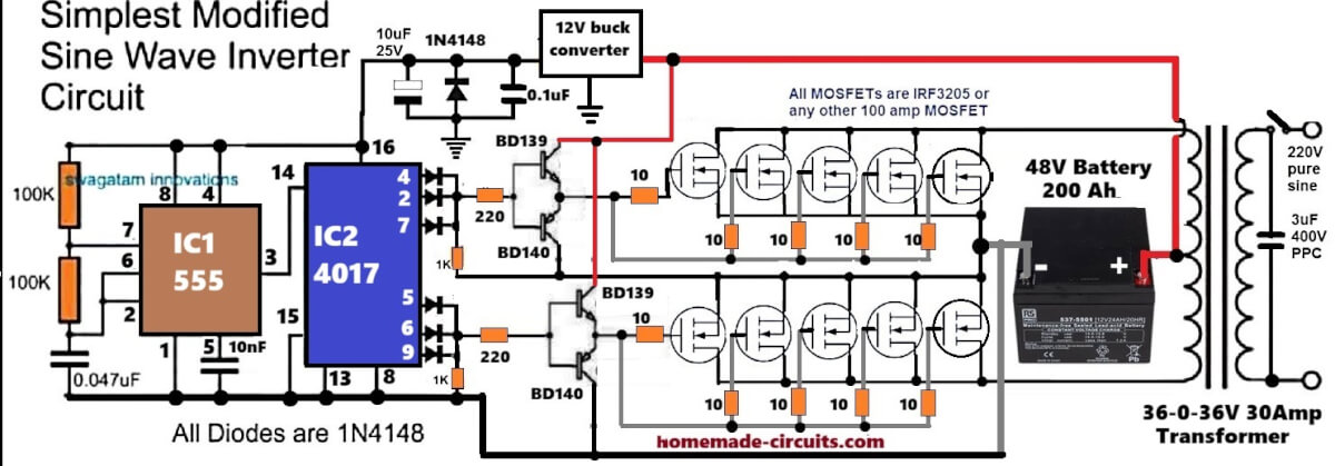
In basic setup all drains join together, all sources join together, and all gates receive same drive signal. So now all MOSFETs try switching together at same time. But practical circuit is never that clean. Extra parts become necessary otherwise instability can start.
Why MOSFETs Are Easier To Parallel Than BJTs
MOSFETs are actually nicer than BJTs for parallel work because MOSFET has this behavior where RDS(on) rises with temperature. So if one MOSFET starts taking more current then it heats up and once temperature rises then its resistance also rises slightly, therefore current comes down a bit.
Meanwhile cooler MOSFET nearby starts taking little more current. Kind of self balancing happens naturally.
BJTs do opposite thing, hotter transistor may start taking even more current and then thermal runaway can happen very fast.
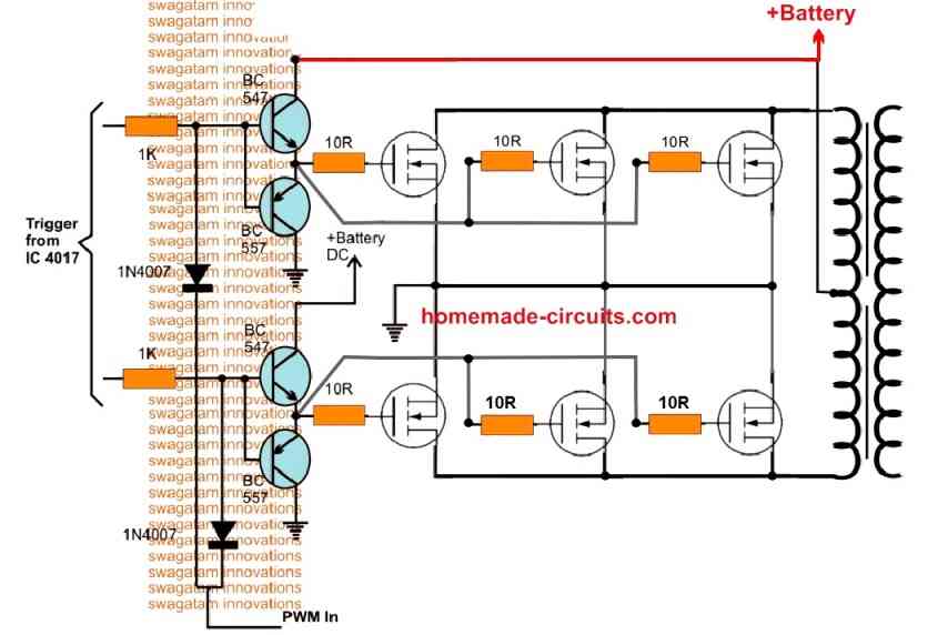
Importance Of Individual Gate Resistors
This is where many beginners make mistake. They connect all MOSFET gates directly together with one common resistor or sometimes no resistor also.
This gives rise to gate ringing, oscillation, unequal switching, and parasitic effects start troubling. Correct way is separate resistor for each MOSFET gate.
Driver output to gate resistor then to individual gate.
Usually values like, 4.7Ω, 10Ω, 22Ω, something around these are used depending on frequency and MOSFET gate capacitance.
Each MOSFET behaves slightly differently, one may switch faster, another slower. One may have little different gate charge, so without separate resistors they start affecting each other badly.
Separate gate resistors stabilize things down.
Gate Driver Requirements For Parallel MOSFETs
Now as MOSFET count increases, total gate capacitance also becomes huge.
Then weak driver can not charge discharge gates quickly. Hence switching becomes slow, increasing heat, switching losses, and sometimes cross conduction trouble also arises.
That is why strong MOSFET drivers are used.
Common ones are:
- TC4420
- TC4429
- IR2110
- IR2184
- UCC21520
- HCPL-3120
These can push and pull several ampere current into MOSFET gates fast and quick.
Push-Pull Gate Driver Stages
Many practical circuits also put push pull transistor stage between controller and MOSFET gate. Very common pair is:
- BD139
- BD140
This pair gives stronger gate charging and discharging current. Fast charging helps during turn ON, fast discharging helps during turn OFF, therefore switching losses reduce.
Importance Of Gate-Source Zener Diodes
In high power systems nasty voltage spikes can appear at MOSFET gate because of transformer leakage inductance, wiring inductance, high dv/dt, Miller capacitance effects etc and many other things.
Sometimes gate voltage may exceed safe limit. So people connect zener diode directly across gate and source.
Usually, 15V zener, 18V zener. That zener clamps gate voltage and protects thin gate oxide layer from damage. Very important especially in SPWM inverter side and high voltage bridge circuits.
PCB Layout Is Extremely Important
Many MOSFET failures actually come from bad PCB layout, not from schematic mistake.
At high switching current even small PCB inductance can create dangerous spikes. So gate tracks should stay short, copper tracks thick, layout symmetrical as much possible. Source return path also should stay short. Power ground and signal ground should not get mixed randomly. Driver bypass capacitors should remain close to driver IC itself.
Small layout mistake sometimes destroys full MOSFET bank, we see that many times.
Current Sharing Between Parallel MOSFETs
Perfect current sharing never happens fully.
One MOSFET always takes slightly more or less current because of PCB resistance, timing differences, temperature differences, device variations, and many such small things. So to improve sharing then use identical MOSFETs only, same gate resistors, same track lengths, symmetrical layout.
In very high current systems people sometimes add tiny source balancing resistors also.
Sharing Current in Parallel MOSFETs
For example, if inverter runs from 48V battery side then current becomes very high.
5kVA ÷ 48V ≈ 104A
But that is only simple calculation side, real current goes higher because inverter also has losses and surge load moments, so now current can easily touch around 120A to 150A or something near that.
Now one single MOSFET cannot comfortably handle this much current, heating becomes too much, stress also increases, therefore we put many MOSFETs in parallel at each switching section. So normally people use something like:
3 MOSFETs parallel, or 4 MOSFETs parallel, sometimes even 6 MOSFETs together, depending on MOSFET current rating, heatsink size, cooling fan condition and all that practical side.
So in full bridge inverter then every section has parallel MOSFET group only.
- Upper left side = many MOSFETs together
- Lower left side = many MOSFETs together
- Upper right side = many MOSFETs together
- Lower right side = many MOSFETs together
Now about MOSFET choosing side, low RDS(on) MOSFETs are better because resistance stays lower when MOSFET switches ON, therefore heating reduces and power loss also stays less.
Some MOSFETs which people use a lot in high power inverter work are:
- IRFP260N
- IRFP2907
- IRFB4110
- HY4008
- HY5608
- IXFH series MOSFETs
Voltage rating also must be selected carefully, we cannot use very close voltage rating otherwise MOSFET may puncture during spikes. So always keep enough safety margin above DC bus voltage.
For example, in 48V systems people usually use around 75V to 100V MOSFETs. If DC bus is around 160V then 200V MOSFETs are commonly used. And for 310V bus side, generally 500V or 600V MOSFETs are used because spikes also come there, so lower voltage MOSFET becomes risky.
Heat Sink Requirements
Even with many MOSFETs together, heat can still become huge. So proper heatsink is compulsory. Thermal paste should be applied properly, add insulation pad also if needed, and for big systems forced air cooling also becomes necessary.
Without thermal management parallel MOSFET bank may fail very quickly.
RC Snubber Networks
Many high power MOSFET circuits also use RC snubber network. Typical one may have, 47Ω resistor, 47nF to 100nF capacitor in series. This absorbs switching spikes and reduces ringing a bit. Also helps reduce EMI and protects MOSFET side. Becomes especially useful when transformer or inductive load is connected.
Dead Time Considerations
In H-bridge, full bridge inverter, half bridge converter type circuits, dead time becomes extremely important.
Meaning upper MOSFET should fully switch OFF first, then only lower MOSFET turns ON. Otherwise both may conduct together for tiny moment and direct short circuit happens across supply. That condition is called shoot through, and MOSFETs can explode almost instantly sometimes.
Choosing The Correct MOSFET
MOSFET selection depends on voltage rating, current rating, RDS(on), gate charge, switching speed, thermal resistance, all these things.
For low voltage systems like 12V to 48V, usually 75V, 100V, 150V MOSFETs are common because low RDS(on) types are available there. For high voltage DC bus systems like 160V to 400V, then 250V, 500V, 600V MOSFETs may become necessary depending on topology.
Common Mistakes In Parallel MOSFET Designs
Very common mistakes are:
- no separate gate resistors
- weak gate driver
- long gate tracks
- bad grounding
- poor heatsinking
- unequal PCB layout
- missing bypass capacitors
- no snubber network
- less dead time
Then people wonder why MOSFETs keep failing randomly even though schematic looked okay.
Calculator Tool
Conclusion
Parallel MOSFET connection is very powerful for heavy current applications but simply joining many MOSFETs together is not enough.
Gate driving, PCB layout, gate resistors, zener protection, snubber network, cooling, all these matter heavily.
If done properly then parallel MOSFET bank can handle very large current quite reliably in inverter systems, SMPS, motor drives, industrial converters and many other high power circuits.


Questions & Answers
Hello Swagtam. Appreciate your instructions. Please, how is it possible to double the transistor pairing for the commercially available 1000w zvs driver? will doubling the transistor pair enable me to reach higher temperatures more quickly and comfortably?Or is it better to build one from scratch? https://www.homemade-circuits.com/zvs-induction-heater-tank-calculator/
Hi Simon,
No…Just soldering extra transistor onto a commercial 1000W board will likely cause them to overheat and burn out instantly due to gate drive limitation and timing mismatche.
Doubling transistor alone does not increase heating speed or temperature power delivery is governed by supply voltage, coil design and the tank components.
It is highly recommended to either build a custom circuit from scratch using dedicated gate driver ICs and proper layout technique, or upgrade to a higher rated commercial unit made from the factory for higher power levels.