In this post I have explained about MOSFET bidirectional power switches, which can be used for operating a load across two points bidirectionally. This is simply done by connecting two N-channel, or P-channel MOSFETs back to back in series with the specified voltage line.
What is a Bidirectional Switch
A bidirectional power switch (BPS) is an active device built using MOSFETs or IGBTs, which allows a two way bidirectional flow of current when powered ON, and blocks a bidirectional flow of voltage when powered OFF.
Since it is able to conduct across both ways, a bidirectional switch can be compared and symbolized as a normal ON/OFF switch as shown below:
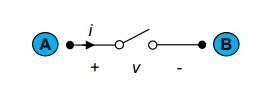
Here, we can see a positive voltage is applied at point "A" of the switch and a negative potential is applied at point "B", which allows the current to flow across "A" to "B". The action can be reversed by simply changing the voltage polarity. Meaning, the points "A" and "B" of the BPS can be used as interchangeable input/output terminals.
The best application example of a BPS can be seen in all MOSFET based commercial SSR designs.
Characteristics
In Power Electronics, the characteristics of a bidirectional switch (BPS) is defined as a four-quadrant switch having the ability to conduct positive or negative current in the ON-state, and also block positive or negative current in OFF-state. The four-quadrant ON/OFF diagram for a BPS is shown below.
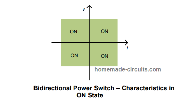
In the above diagram, the quadrants are indicated in green color which indicates the ON state of the devices regardless of the polarity of the supply current or the waveform.
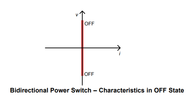
In the above diagram, the red straight line indicates that the BPS devices are in OFF state and offers absolutely no conduction regardless of the polarity of the voltage or the waveform.
Main Features a BPS Should Have
- A bidirectional switch device must be highly adaptable to enable easy and quick power conduction from both sides, that is across A to B and B to A.
- When used in DC application, a BPS must exhibit minimum on state resistance (Ron) for improved voltage regulation of the load.
- A BPS system must be equipped with proper protection circuitry to withstand sudden in rush current during a polarity change, or at relatively high ambient temperature conditions.
Bidirectional Switch Construction
A bidirectional switch is constructed by connecting MOSFETs or IGBTs back to back in series as shown in the following figures.
Here, we can witness three fundamental methods through which a bidirectional switch can be configured.
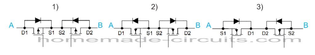
In the first diagram, two P-channel MOSFETs are configured with their sources connected back to back with each other.
In the second diagram, two N-channel MOSFETS can be seen connected across their sources for implementing a BPS design.
In the third configuration, two N-channel MOSFETs are shown attached drain to drain for executing the intended bidirectional conduction.
Simulation
Basic Functioning Details
Let's take the example of the second configuration, in which the MOSFETs are joined with their sources back to back, let's imagine positive voltage is applied from "A", and negative to "B", as shown below:
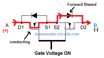
In this case we can see that when the gate voltage is applied, current from "A" is allowed to flow through left MOSFET, then through the internal forward biased diode D2 of the right side MOSFET, and finally the conduction completes at point "B".
When the voltage polarity is reversed from "B" to "A" the MOSFETs and their internal diodes flip their positions as shown in the following illustration:
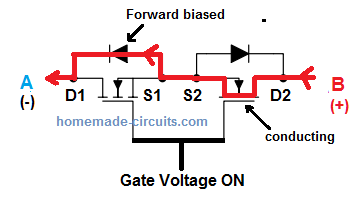
In the above situation, the right side MOSFET of the BPS switches ON along with D1 which is the internal body diode of the left side MOSFET, to enable the conduction from "B" to "A".
Making Discrete Bidirectional Switches
Now I have explained how a bidirectional switch can be built using discrete components for an intended two way switching application.
The following diagram shows the basic BPS implementation using P-channel MOSFETs:
Using P-Channel MOSFETS
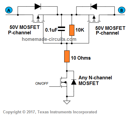
When point "A" is positive, the left side body diode gets forward biased and conducts, followed by the right side p-MOSFET, to complete the conduction at point "B".
When point "B" is positive, the opposite side respective components become active for the conduction.
The lower N-channel MOSFET is controls the ON/OFF states of the BPS device through appropriate ON/OFF gate commands.
The resistor and the capacitor protect the BPS devices from a possible in rush current surge.
However, using P-channel MOSFET is never the ideal way of implementing a BPS due to their high RDSon. Therefore these might require bigger and costlier devices to compensate against heat and other related inefficiencies, compared to N-channel based BPS design.
Using N-Channel MOSFETS
In the next design we see an ideal way of implementing a BPS circuit using N-channel MOSFETs.
In this discrete bidirectional switch circuit, back-to-back connected N-chanel MOSFETs are used. This method demands an external driver circuit for facilitating the two way power conduction from A to B and in reverse.
The Schottky diodes BA159 are used to multiplex the supplies from A and B to activate the charge pump circuit, so that the charge pump is able to generate the necessary amount turn ON voltage for the N-channel MOSFETs.
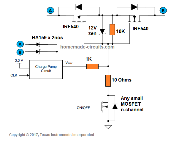
The charge pump could be built using a standard voltage doubler circuit or a small boost switching circuit.
The 3.3 V is applied for powering the charge pump optimally, while the Schottky diodes derive the gate voltage directly from the respective input (A/B) even if the input supply is as low as 6 V. This 6 V is then doubled by the charge ump for the MOSFET gates.
The lower N-channel MOSFET is for controlling the ON/OFF switching of the bidirectional switch as per desired specifications.
The only disadvantage of using an N-channel MOSFET compared to the previously discussed P-channel are these extra components that may consume extra space on the PCB. However, this disadvantage is outweighed by the low R(on) of the MOSFETs and highly efficient conduction, and low cost small sized MOSFETs.
That said, this design also does not provide any effective protection against over heating, and therefore oversized devices may be considered for high power applications.
Conclusion
A bidirectional switch can be quite easily built using a couple back to back connected MOSFETs. These switches can be implemented for many different applications which require a bidirectional switching of the load, such from AC source.
References:
TPS2595xx, 2.7 V to 18 V, 4-A, 34-mΩ eFuse With Fast Overvoltage Protection Data Sheet


Questions & Answers
Hi Swagatam,
Thank you for your explain.
I would have a question, in “Basic Function Details” part, you explained that the current will be followed through body diode. However, if both switches are turned on, why the current still follows through body diode instead of channel of MOSFET. Hope to received your feedback. Thank you very much
Hi Huy,
If both MOSFETs are ON, one gets reversed biased to the specific AC cycle, so the “body diode” of only that MOSFET conducts in reverse.
want to design 110 V and 220V, 5 A DC voltage supply. Will you help with any circuit?
Please provide further details about your requirement..
Hi,
I want to make this bidirectional switch for cell balancing circuit.
Can you help?
Hi, please provide more details about your circuit, if possible I will try to figure it out…
Hi, i am intrested in the Multiplexer circuit with mosfet or diodes i.e a common line should be driven by two inputs, they wont be available simultaneously, so no need to have the select line similar to digital multiplexer. This is basically 30V AC signals multiplexing.
We are having a situation where you want to multiplex two 30V AC signals into a common line. But the thing is, the two input signals will never be present at the same time. So we do not need any select line like digital multiplexer. Now let us see two simple ways how we can do this.
1. Simple Diode OR Circuit Method
We can use two fast recovery diodes for this job. Like UF4007 type diode, because it is good for AC and high voltage, at least 100V rated.
Then we connect Input A to anode of first diode, and Input B to anode of second diode. The cathodes of both diodes are joined together, and this becomes our common output line.
How it works is like this – when Input A is present and Input B is absent, then the diode connected to Input A becomes forward biased and passes the 30V AC to output. Similarly, when Input B is present and Input A is absent, the diode from Input B conducts and gives output. Since they are never both active at same time, there is no conflict.
But we must use diodes which are properly rated for AC voltage and current. Otherwise, they may burn or not work properly.
2. MOSFET Switching Method
Now we can also use MOSFET switches instead of diodes, because this gives lower voltage drop.
What we do is we take two N-channel MOSFETs, and connect them in back-to-back way (Source to Drain and Drain to Source).
Then for each input, we connect one such MOSFET switch. And we permanently bias the Gate of MOSFET to make it always ON, because no select signal is required.
When Input A is present, the corresponding MOSFET conducts and passes the 30V AC to output. Same thing happens for Input B. The back-to-back MOSFET structure makes sure it can handle AC signals in both directions.
Important that we select MOSFETs with Vds rating above 50V and very low Rds(on), so that we have low loss and good performance.
Now which method is better?
We can say that if you want something very simple and cheap, diode OR method is good enough. But if you care for performance and want less voltage drop, then MOSFET switching method is better, though little more complex.
So now let me know that if you want me to design full circuit diagram for any of these methods, then I will do.
Hi! Could this Bidirectional Switch circuit be adapted to be a bidirectional SPDT switch? I mean when the logic in OFF on the control signal, one bidirectional path is allowed, from A to B, for instance. When the logic is OFF on the control signal, the bidirectional path would be from A to C, for instance… Could it be done? Just like a physical relay?
Hi, that may be possible, for this you might need to short circuit the gate/source of the MOSFET which needs to remain disabled.
Is there an available layout for this above Power Mosfet A C Solid state relay ,and or a Gerber file ,so I can order a PCB board to build a prototype.
Because I don’t have any knowledge on Gerber file Generator software .
Thanks
Sorry, PCB details are not available with me, however all the PCB related work can be easily handled by any professional PCB designer.
Also, I would recommend you to first test the design on a perfboard (strip board) by soldering, and proceed with the PCB only if it works satisfactorily:
I just found your article on the DC relay.
“SPDT Solid State DC Relay Circuit using MOSFET”
Thanks Gregg
Ok, thanks for updating the information. Hope the circuit works for you.
I have read your other articles on relays and such.
My question is can I just use DC as the input source and not the ac source?
The relay Im now using is “SRD-05VDC-SL-C 5Pin 5V DC Power Relay 10A 250VAC” and for the most part it works well. I want to replace that one with an homemade SSR or MOSFET’s like in your drawings above.
Thank You Gregg
I want to ask you a question of using P-Channel MOSFETS.How do i calculate and select the capacitance and resistance?
The resistor values are not critical, for the 10k you can use any value between 1k and 10k, for the 10 ohms you can use any value between 5 ohms and 30 ohms. The capacitor is not mandatory, you can use it or leave it.
I’m not sure it’s true or false, I guess :
Your 1) assumption is correct.
2) 10K ensures the MOSFET gates are never floating during the OFF periods. 0.1uF is optional, it helps smooth switching of the MOSFETs
Sorry, If I care P-MOSFET’s Igss and N-MOSFET’s Idss, how do i calculate and select the capacitance and resistance?
The 10 ohm, the 10k and the 0.1uF are absolutely not critical and does not need precise calculations, you can use the same values as shown in the diagram.
Hi Swagatam, Congratulations on the two-way switch, it’s very nice. If you had time to post a switch with MOSFET-N, for reverse polarity protection that would be great, thanks in advance and bless you.
Thank you Johnny, If I happen to find that circuit will surely post it for you.
Hi, how can I apply this design to low-voltage cases? In this design, the input voltage must be higher than the forward voltage of the body diode. However, I need to design an analog switch for low-voltage applications such as 50-100mV. Can you suggest any circuit for that? It will be used for switching the capacitors paralleled with an inductor to change the frequency.
Hi, 50-100mV is very small voltage level and no transistorized bidirectional switch can work with such small voltages.
Instead you can try the following IC which has 4 analog bidirectional switches in it.
https://www.homemade-circuits.com/how-to-connect-ic-4066-in-a-circuit/
Thanks for your reply. 4066 is able to work at the low input voltage. However, it has a high on-state resistance. My design circuit will only work at very low power, such as uA to 1mA level. Can we use discrete components to achieve the function of 4066? I am not very familiar with the inner structure of the 4066, could you please help me?
With such small voltage and current values, designing a discrete bidirectional switch looks very difficult.
You can perhaps try a 4 BJT H-bridge circuit, using PNP transistor on the high side and NPN transistor on the low side.
Here’s an example for an H bridge BJT switching circuit:
How can i simulate two mosfets connected in series? I want to test just to make sure that they work. Im trying to simulate it using falstad.
I am not sure about it because I normally build circuits practically to test them, I don’t use simulators.
12V zener is back to front. A much larger resistor than 10Ohms is needed to protect the N Channel FET as the 12V Zener gives a low resistance path from the supply of it’s above 12V
Hi! Thank you for your very easy to follow article. I have an idea that I would be interested to hear you opinion on: How about driving two N-MOS back to back common source, with a traditional low side mosfet gate driver, fed by a approx 10V higher voltage than the bus voltage? This way the switch can be PWM’ed and also do steady on state. I’m thinking for example a UCC27533 gate driver, fed by a non-isoloted small step up converter, 12V->25V.
Thanks in advance.
Hi, I can’t figure out the answer at this moment, will need to investigate it deeper to get a proper answer.
Hi,
if i apply to your bidirectional switch a low level voltage, ( like 0.4 volt ) it not work a cause of Forward voltage of internal diode. How works the solid state relay, that works also 0.4 volt ?
Sorry for my english !
Hi, can you show me the SSR datasheet where 0.4 V conduction is mentioned.
In the above article if the diodes are replaced with schottky diodes then the drop will be hardly 0.2V
Hi, Swagatam
I’m beginner for electric circuit. In your last figure,
Why is there diode and resistor in parallel between 2 mosfets?
Thanks.
Hi Tommy, the 12 V zener ensures that the gate voltage never exceeds this value regardless of the gate supply input value. The 10K resistor enables the gates of the MOSFETs to be referenced to ground and ensures that the gates are never in the floating condition, which is a recommended practice for all N channel mosfets.
Thanks for your reply, I’ve got another question.
If power source A and B are same DC source like short circuit, how to decide flow direction(polarity) between A and B. I’m not fully understanding about schottky and charge pump relation as well.
It won’t make sense if you use the same DC source for both the A/B points. The enable the current to flow, the A and B must be opposite in polarity, and with a series load, otherwise the current cannot flow.
The schottky diodes derive the voltage from A and B points and feeds them to the gate of the mosfets. If A and B voltage drops below 9V or 6V then the charge pump switches ON and boosts this voltage to higher levels so that the mosfet gates can receive optimal driving voltage. Both of these are optional, and can be replaced with customized gate feeds.
This is a nice explanation, but the current path though the back2back mosfets is just wrong. The reason for putting another mosfet to the first one, instead of just a diode, is having the ability to block reverse current while also minimizing switching losses, because this parasitic body diode is almost always there and will make current flow when positive voltage is put across source-drain path, even if a mosfet is not turned on.
As you stated in a reply to a comment, the switching losses are indeed negligible. But that is because both of the mosfets conduct at the same time and one of the diodes that is forward biased is always bypassed by a conductive channel, depending on the current flow direction.
Thank you, however I cannot see anything wrong in the current path. The diodes actually indicate the body diodes which conduct while the current passes through source to drain.
An already conducting (turned on) mosfet doesn’t have a problem with conducting in both directions, because it does not act like a diode, but a resistor. The source-drain path will either conduct very well (depending on device’s RDSon) when turned on, or conduct through the diode even if the mosfet isn’t turned on. The diode will just prevent the voltage from exceeding a dangerous negative value on the drain in reference to source and that’s about it.
And depending on a body diode in a design isn’t usually bad practice. They are quite heavy-duty, especially in power mosfets, usually having the same rating as the mosfet itself.
Yes that’s correct but the diode being forward biased will provide a better free path to the current, so that the current ignores the MOSFET and takes the easier path through the diode. If you connect a resistor and a diode in parallel the current will pass through the diode and not the resistor.
Sure, that would be correct. Unless the resistor is in the milliohms range for a lower voltage power mosfet, meaning dozens of amps need to flow (if the datasheet allows that) to create a drop significant enough to make the diode open and start conducting.
But who would want their saturated mosfet to create such a drop?
You are correct???? A MOSFET is on in both directions. The body diode only conducts when it’s off. Two MOSFETs are needed only when blocking is needed in both directions.