SSR or Solid state relays are high power electrical switches that work without involving mechanical contacts, instead they use just a couple of solid state semiconductors like MOSFETs for switching an electrical load, smoothly, and with high efficiency.
SSRs can be used for operating high power loads, through a small input trigger voltage with negligible current.
These devices can be used for operating high power AC loads as well as DC loads.
Solid State Relays are highly efficient compared to the electro-mechanical relays due to a few distinct features.
Main Features and Advantages of SSR
The main features and advantages of solid state relays or SSRs are:
- SSRs can be built easily using a minimum number ordinary electronic parts
- They work without any form of clicking sound due to the absence of mechanical contacts.
- Being solid state also means SSRs can switch at much faster speed than the traditional electro-mechanical types.
- SSRs do not depend external supply for switching ON, rather extract the supply from the load itself.
- They work using negligible current and therefore do not drain battery in battery operated systems. This also ensures negligible idle current for the device.
Basic SSR Working Concept using MOSFETs
In one of my earlier posts I explained how a MOSFET based bidirectional switch could be used for operating any desired electrical load, just like a standard mechanical switch , but with exceptional advantages.
The same MOSFET bidirectional switch concept could be applied for making an ideal SSR device.
For a Triac based SSR please refer to this post
Basic SSR Design
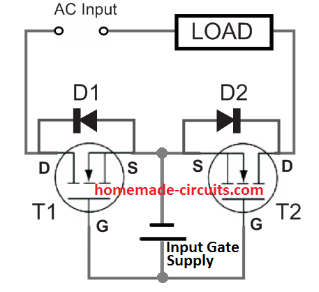
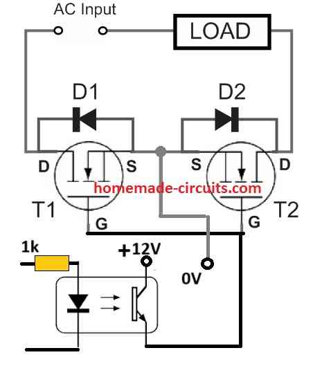
In the above shown basic SSR design, we can see a couple of appropriately rated MOSFETs T1 and T2 connected back to back with their source and gate terminals joined in common with each other.
D1 and D2 are internal body diodes across the drain/source of the respective MOSFETs.
An input DC supply can also be seen attached across the common gate/source terminals of the two MOSFETs. This supply is used for triggering the MOSFETs ON or for enabling permanent switch ON for the MOSFETs while the SSR unit is operational.
The AC supply which could be up to grid mains level and the load are connected in series across the two drains of the MOSFETs.
How it Works
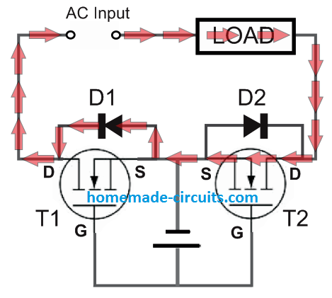
The working of the proposed sold state relay can be understood by referring to the following diagram, and the corresponding details:
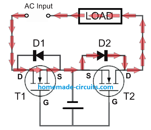
With the above setup, due to the input gate supply connected, T1 and T2 are both in the switched ON position.
When the load side AC input is switch ON, the left diagram shows how the positive half cycle conducts through the relevant MOSFET/diode pair (T1, D2) and the right side diagram shows how the negative AC cycle conducts through the other complementing MOSFET/diode pair (T2, D1).
In the left diagram we find one of the AC half cycles goes through T1, and D2 (T2 being reverse biased), and finally completes the cycle via the load.
The right side diagram shows how the other half cycle completes the circuit in the opposite direction by conducting through the load, T2, D1 (T1 being reversed biased in this case).
In this way the two MOSFETs T1, T2 along with their respective drain/source body diodes D1, D2, allow both the half cycles of the AC to conduct, powering the AC load perfectly, and accomplishing the SSR role efficiently.
Here's an excerpt from the datasheet of the article.

Video showing the testing of the above SSR circuit
Making a Practical SSR Circuit
Why We Use Two MOSFETs For AC
When we want to switch AC using MOSFETs then we find that a single MOSFET cannot block current in both directions because of its body diode.
So we use two N Channel MOSFETs and we connect their sources together and we keep their drains toward the AC line terminals.
When we do this arrangement then the body diodes oppose each other and the AC can be fully blocked when the gate drive is zero. So the pair works like an AC switch.
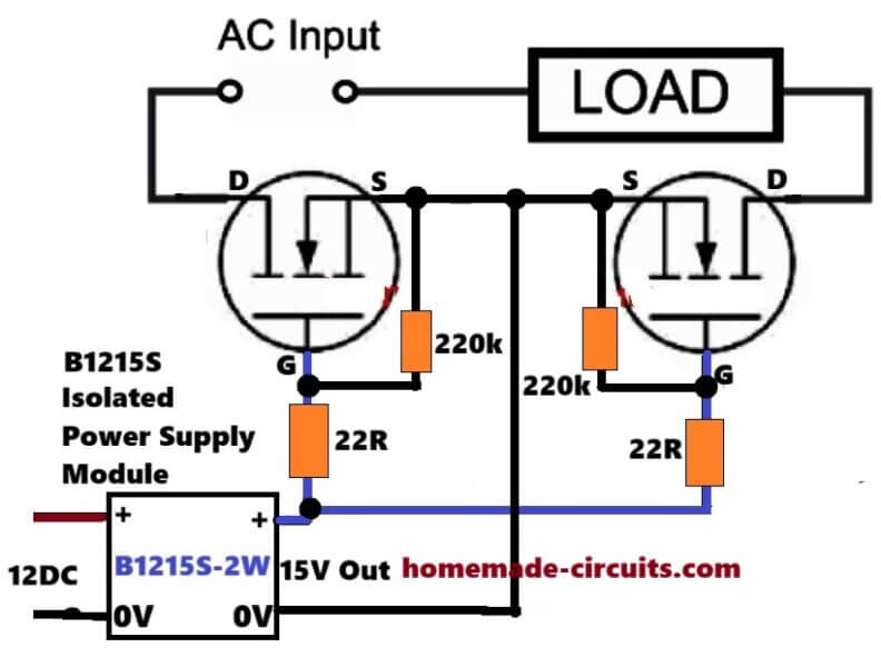
Why We Need A Floating 15 V Supply
When we use back to back MOSFETs in AC circuits then the common source point does not stay at ground level.
This point keeps moving up and down with the AC waveform, so now we understand that the gate voltage also must follow this moving point, because the MOSFET only cares about the Vgs difference.
When the source rises, then gate must rise above it, when the source falls, then gate must fall above it.
So we need an isolated 15 V supply that floats along with the MOSFET sources.
When the supply is floating, then it does not care about earth or neutral and it simply rides with the circuit, so the MOSFET always sees a correct gate voltage.
Why The Source Node And The 15 V Negative Can Touch
Many people think that isolation is broken when the isolated supply negative is connected to the MOSFET source node.
But since the isolated supply has no link with mains or earth, it does not matter. It only follows the MOSFETs.
So the 0 V of the 15 V supply becomes the reference for the MOSFET gates and sources.
When we do this connection, everything still stays isolated from the outside world.
How The Gate Is Driven From The 12 V Control Side
We use an opto or a small control section in the 12 V side. When we give 12 V input to this module then the opto transistor pulls the floating 15 V supply positive toward the MOSFET gate through the gate resistor.
When this happens then the MOSFETs get a Vgs of around 12 V and they turn ON.
When we remove the 12 V input then the gate is left without drive and the resistor that we added slowly discharges the gate. When the gate reaches the same level as the source then the MOSFETs turn OFF.
How The Circuit Behaves When AC Passes
When the AC line is connected to the MOSFET drains then common source node becomes a floating midpoint that shifts according to the load and the waveform.
But the gate supply also floats in the same way so the Vgs stays correct.
When we give the 12 V command, then MOSFETs turn ON in both half cycles and the AC flows without restriction.
When the input is removed then the gate falls down through the 1 M resistor and the MOSFETs turn OFF and block both directions due to the anti series body diode configuration.
Why 220k Is Acceptable In This SSR
We use 220k because we do not need ultra fast gate discharge, and because the SSR is not switching at very high speed.
The AC cycle itself is very slow compared to MOSFET switching, so even a 10 ms or 20 ms fall time is perfectly OK. The 220k value also keeps the loading of the 15 V supply to a very small level, but if you want a little faster discharge you can use 100 K also. Both values work fine because the switching is slow.
Final View Of The Completed SSR
So now the whole SSR becomes very simple. Two N Channel MOSFETs are connected source to source, the drains go to AC.
The floating 15 V positive is fed to the gates through individual 22 Ohms.
The floating 15 V negative goes to the common source.
A 220 K resistor is placed between the gates and the sources of each of the MOSFETs.
The isolated 12 V side drives the opto, and the opto connects the 15 V positive to the gate when it receives the command.
Conclusion
So now we get a simple, very easy to understand bidirectional MOSFET SSR which can switch AC efficiently.
The use of the floating 15 V module makes the design work smoothly even when the AC line moves up and down.
The resistors keeps the gate under control.
Source.
Reference: SSR


Questions & Answers
sir, can you help me to design a DC SSR, bidirectional, maximum voltage of SSR 15v DC, but adjustable from 0,5v to 15v, and a current of 10-20A, SSR powered by 12 vDC from 7812, switching adjustable from 0 hz – 100 hz, so Mosfet + Optocoupler based is prefered. 0-15v is isolated from 12v DC, but 0/Ground is common, thanks in advance. i try to built high ampere low voltage, voltage injector, by switching PSU 0-15v to charge and discharge capacitor, so even at 1 vDC, it can deliver maybe 4-5 Amps to heat the shorted component on circuit
Hi Arya,
I have designed the circuit for you…please check the updated diagram at the bottom section of the above article….
Hello, I’m building/have built a circuit that takes a 50hz ac signal from a class ab amplifier circuit and puts it as the ac input to a n channel fet relay as per fig. 3 above. I’m using a fod 3180 as the driver for the fet’s and so far everything works fine. Where I’m having issues is that I’m using a 555 timer to turn on and off the fod 3180 at about 1khz. On the positive half of the cycle the ac is shut off as expected, as a series of steps up and down the waveform; however, the bottom half of the cycle is unaltered, it’s just a negative sine wave.
I have to admit I’m just about at my wits end on this one. Do you have any idea why the negative half cycle doesn’t turn on and off like the positive half?
Thanks for any help you may provide.
Hi, did you connect the sources of the two MOSFETs with the negative (ground) of the IC 555? And I think a MOSFET driver is not required…you can directly feed the pin#3 of Ic 555 with the gates of the two MOSFETs
Hi Swagatam,
No, I didn’t connect the sources to the neutral ground and I used the driver because I thought that I read in the article that when you use N-channel FETs a driver is necessary in order to charge and discharge the gates of the FETs.
Thanks for the advice, I’ll try it and see how that works out. I’ll let you know if it works.
….I think you are right….a gate driver is strictly required for this application.
Please refer to the following post and check the following and read the “Using N-Channel MOSFET” section:
https://www.homemade-circuits.com/bidirectional-switch/
No problem Kurt,
Initially just connect the pin#3 of the IC 555 with the common gates of the MOSFETs, and connect the common sources with the negative or ground of the 555 circuit, also make sure to connect a 1k resistor between the gates and sources of the MOSFETs. A driver is necessary only when the load current is very high…
hie this diagrams are using DC 12v to genarate AC . can you provide me with a diagram which uses DC 400v to genarate AC . thanks
This circuit is not generating AC, it is controlling an AC load.
Hi, having minimal knowledge of electronics, I was wondering if the final circuit would be able to work safely on 240VAC power input and an 800W resistive load.
Hi, the above concepts are recommended only for experts in the field, not for newcomers, so I won’t recommend it to you.
If your load is a resistive load, then it can be simply controlled through a single MOSFET and a bridge rectifier, no need of the above complex design. Let me know if you would like to see the full schematic.
I have a 3d printer hotbed (resistive load 4 x 200W) and this should be controlled using PWM. So I was trying to find a solution for that, and discovered you article which seemed fit for my case. If you think that another simpler circuit, could make it work, I would like to have the schematic.
In any case, thank you for responding!
I think you should try a dimmer switch circuit such as this for PWM controlling of your load:
https://www.homemade-circuits.com/simple-ceiling-fan-regulator-circuit/
Your diagram is completely wrong. I don’t think you know what you’re talking about at all. When the MOSFET is on, current flows through the channel, not the body diode.
I know the current flows through the channel, the main thing is that, does the above concept work as intended in the application, or not.
Hi , I have a question .Is there anywhere I can find a Power mosfet Solid State relay for 20 amps using 120 VAC for sale or at least PCB kit ,maybe even pcb layout with , if possible a GERBER file, so I can order the production of a prototype Mosfet SSr for A C ?
Thanks in advance
Hi, you can try the following modified version of the first circuit:
However, I do not have the PCB details for this design.
Thank you very much !!
Hi sir, hope all is going well. Sir i need your
kind support. I want to make 40amp ssr.can you provide me diagram with components plz as usual in easy way plz
Hi Ghulam, what type of load do to want to control with the SSR, AC load or DC load?
Sir i want to run AC load, i tried with bt136, but as you know bt136 can’t handle heavy load…..i have bta41 800B. So plz guide me with diagram and components which is required. Plz
Thanks
Hi Ghulam, yes you can use BTA41800, it is rated to handle 40 amps load.
I hope you are referring to the following design
Yes sir same i want, sir what is the value of R1?all resister required qaurter watt? Sir can i use moc3021?sir plz guide me with diagram of bta41 800b. I dont have TIC 226 D/M plz
Thanks
Ghulam, R1 can be 1k 1/4 watt if the input voltage is between 5v and 15V.
All other resistors can be 1 watt CFR.
Yes MOC3021 can be also used.
The shown triac can be replaced with your specific 40 amp triac, no issues.
MT1 will go to the R4 side and MT2 will go to the R2 side.
Thank you sir, i will try and update you.
Sure, no problem, Ghulam.
Hello Sir, great document Thank you for everything.
I have a question please, can we use the basic circuit to connect or disconnect a series of 200v photo voltaic panels?
Thank you again sir
Thank you Laurent, you can use the basic circuit to connect or disconnect PV panels, however the above circuits are meant for AC supplies and loads, for DC supplies, like from a PV systems, you can employ a simpler design using a single MOSFET.
Hi , my name is Helder , I am trying to find power Mosfets S S Rs, for a project where I can’t use Triac SSRs, maybe I am looking at wrong places , I just can’t find MOSFET SSRs for A C voltages on AC currents like 10 to 15 amps , any help would be greatly appreciated
Hello Helder, the circuit explained in the above articles specifically designed to handle AC inputs, so you can use the above circuits with AC supply and AC loads.
One minor issue with the explanation of the circuit is whether or not current is conducted mainly through the body diode in the “reverse” MOSFET or whether it goes through the channel. Your second figure suggests that this current goes through the body diode but in most practical circuits, it won’t. The channel of a MOSFET can conduct in both directions when the gate is appropriately biased. Placing a voltage on the gate creates a conducting channel between the drain and source which acts like a low-value resistor. If your gate drive is adequate for the MOSFETs involved and they are sized appropriately for the current, the forward drop across the channel resistance is likely to be far lower than the forward voltage of the body diode, so the diode won’t turn on and will pass negligible current whilst the vast majority of it passes the the channel just like it does in the “forward” MOSFET.
Thank you for your quick response. Sorry to hear you haven’t yet designed one. If and when you do, will I be sent an email letting me know?
No problem! Sure, I will!
Interesting subject. Thank you for requesting questions.
Magnetic switches are essential for power equipment safety (table saws etc). Much of the older equipment, that is still effective, continues to be used but are not so equipped. Magnetic switches are expensive and, I’m sure, could be replaced my electronic ones. Have you designed/made such a switch that might be used for 120v or 240v single phase circuits?
Hall effect sensor and reed relay are the electronic magnetic sensors, but they require an additional electronic circuit to work. I haven’t yet designed a specific circuit using these sensors for the mentioned application.