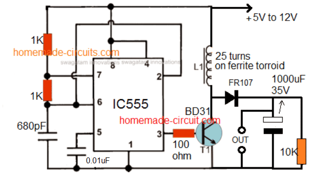
This calculator will help you to design and find the optimal inductor value for a non-isolated boost (step-up) converter circuit, ensuring that your circuit works with an efficient operation with a 30% ripple current.
Boost Converter Inductor Calculator
Calculates required inductance assuming an ideal converter and a 30% target ripple current.
Results:
Duty Cycle (D): 0 %
Estimated Input Current (Iin): 0 A
Optimal Inductor Value (L): 0 µH
How to Use the Boost Converter Inductor Calculator
Steps to Use:
Enter the Input Voltage (Vin) = The voltage from your power source which you want to boost (e.g lets say 12V).
Enter the Output Voltage (Vout) = The desired boosted voltage value which you want at the output (e.g let us say 220V).
Enter the Switching Frequency (kHz) = The PWM switching frequency of your astable multivibrator circuit (e.g you can set it up to work with 50 kHz).
Enter the Output Current (A) = The expected load current, which you want to supply the connected load at the output (e.g 1A).
Click the "Calculate" Button = The results will then show up in the relevant fields:
- Duty Cycle (%) = How long the switch stays ON in one cycle.
- Optimal Inductor Value (µH) = The required inductor size for stable operation.
Example Calculation
Given:
- Vin = 12 V
- Vout = 220 V
- f = 50 kHz = 50,000 Hz
- Iout = 1 A
Step 1: Duty Cycle (D)
Formula:
D = 1 − (Vin / Vout)Substituting:
D = 1 − (12 / 220)
  = 1 − 0.054545
  = 0.945455
Therefore....
D = 94.55%Step 2: Estimated Input Current (Iin)
Formula:
Iin = Iout / (1 − D)Substituting:
Iin = 1 / (1 − 0.945455)
     = 1 / 0.054545
     = 18.33 A
Therefore,
Iin ≈ 18.33 AStep 3: Ripple Current (ΔIL)
If "Input Current (Recommended)" is selected:
ΔIL = 0.3 × Iin
     = 0.3 × 18.33
     = 5.50 A
Step 4: Inductor Value
Formula:
L = (Vin × D) / (ΔIL × f)Substituting:
L = (12 × 0.945455) / (5.50 × 50,000)
  = 11.345 / 275,000
  = 0.00004125 H
Therefore,
L = 41.25 µHFinal Results (Using Ripple Based on Iin)
- Duty Cycle: 94.55%
- Estimated Input Current: 18.33 A
- Ripple Current: 5.50 A
- Optimal Inductor: 41.25 µH
As you can see, the duty cycle is so high at 95% which is a bad thing, so boosting voltage with this circuit from 12V to 220V looks like a bad idea.
So better to go with flyback SMPS topology instead.
Questions & Answers
Please (1) what is the output voltage of this boost converter circuit and (2) where is the battery negative input voltage terminal,only the battery positive terminal voltage (+5 to 12) is indicated in the circuit.I mean where can I connect battery negative wire to for input voltage
You have to decide what output voltage you want…and then calculate accordingly…
The pin#1 line of IC 555 is the ground line or the battery negative line…
Hello Mr. Swagatam, thank you so much for everything you do for us. We are becoming increasingly skilled and very confident in this field of electronics thanks to you and your expertise. But currently, my biggest problem is this: I still haven’t managed to properly size the complete winding of a switching power supply.
Hello NgPark,
Thank you for your kind words, I am glad you found my circuits helpful..
Can you please tell me which circuit and topology have you tried, and what kind of difficulties are you facing? I will try my best to sort it for you…please let me know..
I can’t find BD31 for sale. Is the part number correct?
The transistor number is not critical, you can try any transistor of your choice by appropriately matching the parameters.
I am not a electronic student and a chemistry student. Hence I asked you to give me circuit schematic so that I could directly jump into my experiments. I have a TV LOT of ferrite core and 28 K V output. More over it has a diode builtin its output. So I thought I will wind some wire on the core and get the required voltage.
SO try to understand my problem and give me solution.
Thanks and best regards.
Vyas, I do not know much about the ferrite core used in TV LOT coil, and have no such calculator to calculate a LOT winding.
If you can use a standard ferrite E-core for your boost converter then I can probably help.