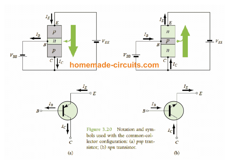
A BJT common collector amplifier is a circuit in which the collector and the base of the BJT share a common input supply, hence the name common collector.
In our previous articles we have learned the other two transistor configurations, namely the common-base and the common-emitter.
In this article I have explained the third and the final design which is called the common-collector configuration or alternatively it is also known emitter-follower.
The image of this configuration is shown below using the standard current flow directions and voltage notations:
Main Feature of Common Collector Amplifier
The main feature and the purpose of using a BJT common collector configuration is impedance-matching.
This is due to the fact that this configuration possesses a high input impedance and a low output impedance.
This feature is actually the opposite of the other two counterparts common-base an common-emitter configurations.
How Common Collector Amplifier Works
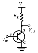
From the figure above we can see that the load here is attached with the emitter pin of the transistor and the collector is connected to a common reference with respect to the base (input).
Meaning, the collector is common to both the input and the output load. In other words, the supply coming to the base and the collector both share the common polarity. Here, the base becomes the input and the emitter becomes the output.
It would be interesting to note that, although the configuration resembles our previous common-emitter configuration, the collector can be seen attached with the "Common Source".
With regards to the design features, we don't have to incorporate the set of common collector characteristics for establishing the circuit parameters.
For all practical implementations, the output characteristics of a common-collector configuration will be exact as attributed for the common-emitter
Therfeore, we can simply design it by using the characteristics employed for the common-emitter network.
For every common-collector configuration, the output characteristics are plotted by applying IE vs VEC for the available IB range of values.
This implies that the both common-emitter and common-collector have identical input current values.
For achieving the horizontal axis for a common-collector, we just need to change the polarity of collector-emitter voltage in a common-emitter characteristics.
Finally, you will see that there's hardly any difference in the vertical scale of a common-emitter IC, if this is interchanged with IE in a common-collector characteristics, (since ∝ ≅ 1 ).
While designing the input side, we can apply the common-emitter base characteristics in order to achieve the essential data.
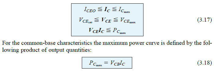
Limits of Operation
For any BJT the limits of operation refers to the operational region over its characteristics which indicate its maximum tolerable range and the point where the transistor can work with minimum distortions.
The following image shows how this is defined for BJT characteristics.
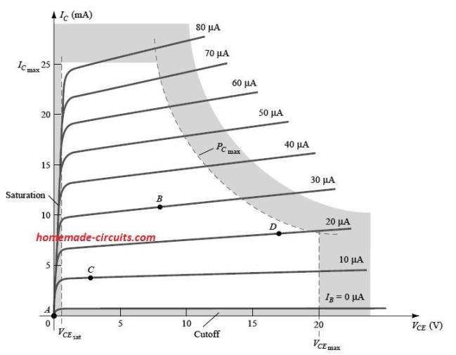
You will also find these limits of operation on all transistor datasheets.
A few of these limits of operation are easily understandable, for example we know what is maximum collector current (referred to as continuous collector current in datasheets), and maximum collector-to-emitter voltage (typically abbreviated as VCEO in datasheets).
For the example BJT demonstrated in the above graph, we find IC(max) is specified as 50 mA and VCEO as 20 V.
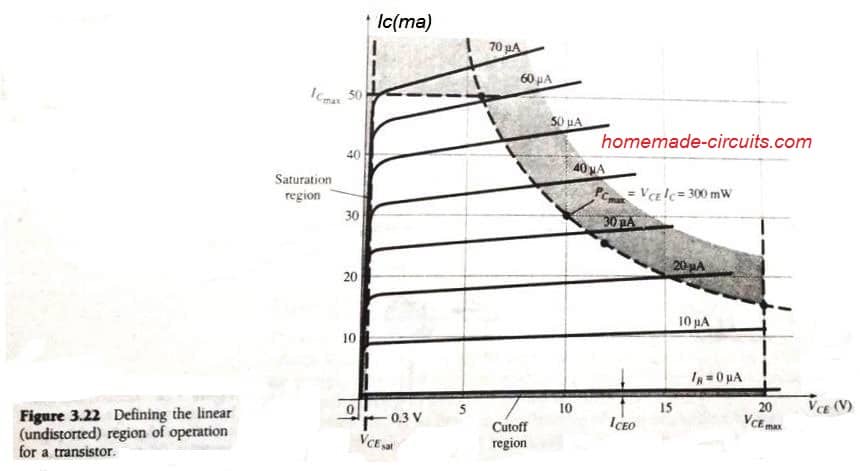
The vertical line drawn indicated as VCE(sat) on the characteristic , exhibits the minimum VCE which can be implemented without crossing the non-linear region, indicated with the name "saturation region".
The VCE(sat) specified for BJTs is normally around 0.3V.
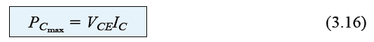
The highest possible dissipation level is calculated using the following formula:
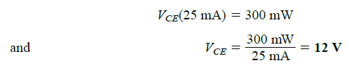
In the above characteristic image, the assumed BJT's collector power dissipation is shown as 300mW.
Now the question is, what is the method through which we can plot the curve for the collector power dissipation, defined by the following specifications:
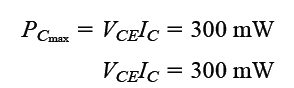
This implies that the product of VCE and IC must be equal to 300mW, at any point on the characteristics.
If suppose IC has a maximum value of 50mA, substituting this in the above equation gives us the following results:
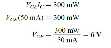
The above results tells us that if IC = 50mA, then VCE will be 6V on the power dissipation curve, as proven in Fig 3.22.
Now if we pick VCE with the highest value of 20V, then the IC level will be as estimated below:
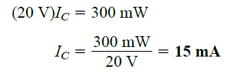
This establishes the second point over the power curve.
Now if we select a level of IC around the mid-way, let's say at 25mA, and apply it on the resultant level of VCE, then we get the following solution:
The same is proven in Fig 3.22 also.
The 3 points explained can be effectively applied for getting an approximate value of the actual curve. No doubt we can use more number of points for the estimation and get even better accuracy, nevertheless an approximate becomes just enough for most applications.
The area that can be seen below IC = ICEO is called the cut-off region. This region must not be reached to ensure a distortion free working of the BJT.
Datasheet Reference
You will see many datasheets only providing the ICBO value. In such situations we can apply the formula
ICEO = βICBO. This will help us to get an approximate understanding regarding the cut-off level in the absence of the characteristic curves.
In cases where you are unable to access the characteristic curves from a given datasheet, it may be imperative for you to confirm that the values of IC, VCE, and their product VCE x IC remain within the range as specified in the following Eq 3.17.
Summary
The common collector is a well known transistor (BJT) configuration among the other three basic ones, and is used whenever a transistor is required to be in the buffer mode, or as a voltage buffer.
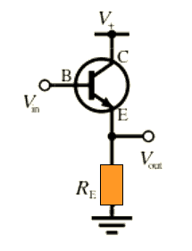
How to Connect a Common Collector Amplifier
In this configuration the base of the transistor is wired for receiving the input trigger supply, the emitter lead is connected as the output, and the collector is hooked up with the positive supply, such that the collector becomes a common terminal across the base trigger supply Vbb and the actual Vdd positive supply.
This common connection gives it the name as common collector.
The common collector BJT configuration is also called the emitter follower circuit due to the simple reason that the emitter voltage follows the base voltage with reference to the ground, meaning the emitter lead initiates a voltage only when the base voltage is able to cross the 0.6V mark.
Therefore, if for example the base voltage is 6V, then the emitter voltage will be 5.4V, because the emitter has to provide a 0.6V drop or leverage to the base voltage for enabling the transistor to conduct, and hence the name emitter follower.
In simple terms, the emitter voltage will be always less by a factor of around 0.6V than the base voltage because unless this biasing drop is maintained the transistor will never conduct. Which in turn means no voltage can appear at the emitter terminal, therefore the emitter voltage constantly follows the base voltage adjusting itself by a difference of around -0.6V.
How Emitter Follower Works
Let's assume we apply 0.6V at the base of a BJT in a common collector circuit. This will produce zero voltage at the emitter, because the transistor is just not fully in the conducting state.
Now suppose this voltage is slowly increase to 1V, this may allow the emitter lead to produce a voltage that may be around 0.4V, similarly as this base voltage is increased to 1.6V will make the emitter to follow up to around 1V....this shows how the emitter keeps following the base with a difference of around 0.6V, which is the typical or the optimal biasing level of any BJT.
A common collector transistor circuit will exhibit a unity voltage Gain, which means the voltage gain for this config is not too impressive, rather just on par with the input.
Mathematically the above may be expressed as:
PNP version of the emitter follower circuit, all polarities are reversed.
Even the smallest of the voltage deviations at the base of a common collector transistor is duplicated across the emitter lead, which to an extent is dependent on the gain (Hfe) of the transistor and the resistance of the load attached).
The main benefit of this circuit is its high input impedance feature, which allows the circuit to perform efficiently regardless of the input current or the load resistance, meaning even huge loads can be efficiently operated with inputs having minimal current.
That's why a common collector is used as a buffer, meaning a stage which efficiently integrates high load operations from a relatively weak current source (example a TTL or Arduino source)
The high input impedance is expressed with the formula:

and the small output impedance, so it can drive low-resistance loads:
Practically seeing, the emitter resistor could be significantly larger and can therefore be ignored in the above formula, which finally gives us the relationship:
Current Gain
The current gain for a common collector transistor configuration high, because the collector being directly connected with the positive line is able to pass the full required amount of current to the attached load via the emitter lead.
Therefore if you are wondering how much current an emitter follower would be able to provide to the load, rest assured that won't be an issue as the load would be always driven with an optimal current from this configuration.
Example Application Circuits for BJT Common collector
Some of the classic examples of emitter follower or common collector transistor application circuits may be seen in the following examples.
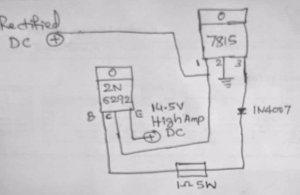
100 amp Variable Voltage Power Supply Circuit
DC Cell Phone Charger Circuit Using a Single Transistor
Single Transistor High Current Battery Charger Circuit

Questions & Answers
Appreciate this post. Will try it out.
Hi, I wish for to subscribe for this web site to get latest updates, so where can i do it please help.
Please find the link at the end of any article post
but pls y is the input mode different in some CC diagram, some is between emitter-base, while other is between collector to base. Will there not be different effect?.
And secondly, I thought that in a common collector mode, the collector was supposed to be common between input and output, so y is the emitter left to be common in some diagrams
I can’t say about other diagrams, but the data given in the above article is the CORRECT one, and a common collector or an emitter follower should be exactly as given above…..