In this post I have explained s few simple DC to DC buck-boost converter circuits which can be used for either stepping up the input DC voltage or stepping down the input DC voltage to specific output DC voltage levels.
Since a buck-boost converter allows the input voltage to be either stepped up or stepped down, hence it is named as buck and boost converter or buck-boost converter.
Basic Working principle
The basic working principle of a buck-boost converter can be understood with the help of the following explanation.
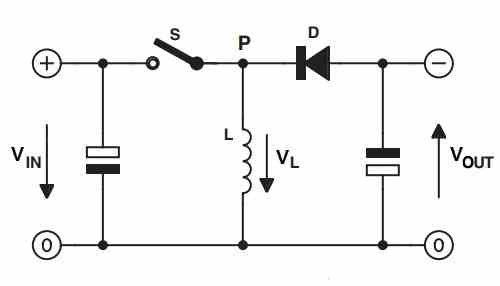
Referring to the basic buck-boost topology diagram above, when the switch S is closed, the input voltage VIN is blocked by the diode D, since D is reverse biased. Therefore the voltage has no other option but to flow through the inductor L.
The inductor L due to its inherent reluctance property initially tries to block the current. Due to this, initially the voltage drop across L is high. However, slowly as the reluctance of the coil decreases and the current through the inductor increases.
During this phase the inductor L stores the energy (voltage and current) inside its winding.
Ideally this the point when the switch S needs to be opened.
When switch S is now opened, the voltage VL stored inside the inductor reverses direction, and it passes through the diode D which is now forward biased. In the process VL also passes through the output capacitor and charges it fully.
During this phase the output capacitor stores energy inside it and gets fully charged, simultaneously the load across VOUT also gets the energy from the inductor for ts operation.
Next, at this point if the switch is closed again, the process repeats as explained above, however now the capacitor provides its stored energy to the load.
Depending how how fast or how slow the switch S is closed and opened, the output DC can be a stepped up or boosted output, or it can be a stepped down or buck output.
In a real life electronic buck-boost circuit, the switch S is replaced with a BJT or a MOSFET and this device is switched ON/OFF through an external PWM for generating a buck or a boost output.
Simple Two Transistor Buck-Boost Converter Circuit
The following figure shows how a very simple buck-boost converter could be built using just a couple of transistors and a few other passive parts.
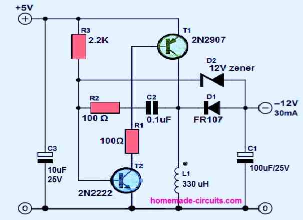
The working of the circuit can be understood from the following points:
Here the circuit is configured to provide a negative boosted output from a 5V input to a -12V output.
As soon as the circuit is powered, the T2 switches ON via R3. This allows T1 to also switch ON through the negative base bias received via R1 and T2.
This causes the full +5V to be applied across the inductor L1 via the collector of T1.
The inductor, due to it reluctance opposes the instant rise in current across it and in the process begins storing energy inside its winding.
Now, slowly the inductor reluctance drops and it starts passing more and more current through. Due to this the base current of T2 is pulled to ground through the inductor and via R2 and C2.
This causes T2 to shut off momentarily.
Now, the stored energy inside the inductor is released back to the output across C1.
C1 now charges fully and simultaneously the output is also supplied with a negatively boosted voltage.
The 12 V diode makes sure that the inverted output boosted voltage does not rise above -12V.
Subsequently C2 begins charging until it is fully charged, which allows T2 to switch ON again, and the process repeats. This repetition process continues at a high frequency.
The frequency of the converter is determined basically by the values of R2 and C2.
By appropriately tweaking the values of R2 and C2, this two transistor circuit could be optimized either to work like a buck converter or a boost converter.
Using IC 555 for the Buck-Boost
This highly efficient and effective buck-boost circuit using the work horse IC 555 would allow you to convert an input source voltage to any required degree, either bucked or boosted, as desired.
We have already learned the concept comprehensively through one of my previous articles where I have explained the versatility of this buck-boost type of topology.
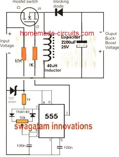
As shown in the circuit diagram below (click to enlarge) the configuration is basically a combination of two distinct stages, viz the upper buck-boost converter stage and the lower IC 555 PWM controller stage.
The buck-boost stage consists of a mosfet which acts like a switch, the inductor which is the main power converting component, the diode which just like the mosfet forms a complementary switch, and the capacitor quite like the inductor forms a complementary power converter device.
The mosfet needs to operate through pulsed triggering so that it alternately switches the input voltage ON and OFF across the inductor in response to its gate voltage.
Therefore the gate voltage should also be in a pulsed form which is accomplished through a IC555 PWM generator stage.
Circuit Operation
The associated IC555 PWM generator is integrated to the mosfet for accomplishing the above discussed operation.
During the ON time of the mosfet, the input voltage is allowed to pass through the mosfet and is applied right across the inductor.
The inductor owing to its inherent property tries to counter this sudden infliction of current by absorbing and storing the power in it.
During the subsequent OFF period of the mosfet, the input voltage is shut off by the mosfet, the inductor now experiences a sudden change in current from peak to zero. In response, the inductor counters this by reversing its stored power across the output terminals via the diode which now acts in the forward biased condition.
The above power from the inductor appears with opposite polarity across the output where the intended load is connected.
The capacitor is positioned to store a portion of the power in it, so that it can be used by the load during the ON time of the mosfet when the diode is reverse biased and power cut off across the load.
This heps to maintain a steady and stable voltage across the load during both ON and OFF cycles of the mosfet.
Using PWM as the Controller
The level of voltage, whether it's a boosted voltage or bucked voltage depends upon how the mosfet is controlled by the PWM generator.
If the mosfet is optimized with higher ON time than the OFF time then the output would generate boosted voltage and vice versa.
However there may be a limit to this, care must be taken not to exceed the ON time beyond the full saturation time of the inductor, and the OFF time must not be below the minimum saturation time of the inductor.
For instance suppose it takes 3ms for the inductor to become fully saturated, the ON time in this case can be set within 0 - 3ms, and not beyond that, This will result in a boost from minimum to maximum depending upon the value of the chosen inductor.
The associated pot wit the IC555 PWM generator can be effectively tweaked for acquiring any desired buck-boost voltage at the output.
The inductor value is a matter of trial and error, try to incorporate as many winding as possible for acquiring better and efficient results and diverse range.
Circuit Diagram
The above design can be suitably upgraded for implementing an automatic output voltage correction with the help of the following modifications:
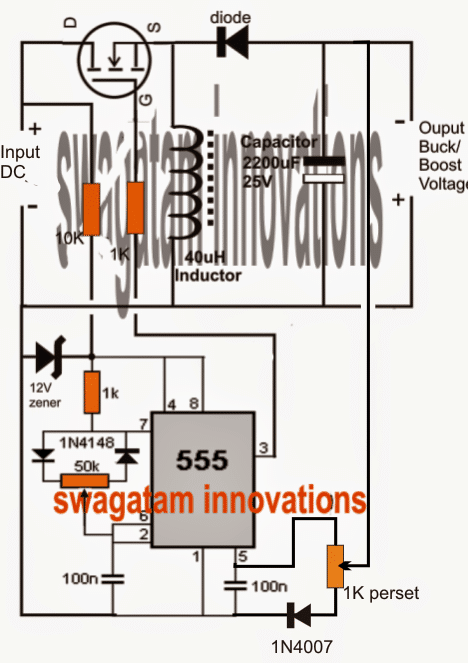
The 1K preset may be appropriately set initially for determining the desired control point.
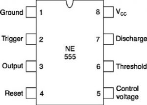
IC 555 Pinouts



Questions & Answers
sir may i know the design considerations of this circuit sir?
Hi Raja,
No critical things are involved, just has to be built as per the given schematic.
Dear Swagatam,
whats the minimum value of input voltage, how much power does the circuit itself consumes and whats the max ampere capacity of the circuit
Dear kkaranjia,
minimum voltage is 5V
the IC will consume 5mA, not sure about the other components, will depend on how the coil and capacitors are optimized.
Max current will depend on the mosfet and inductor ratings, there's no restriction to it.
cant it be modified to run on li-ion battery and give op of 5volt
you will have replace the 555 oscillator with a transistor type oscillator, then it would be possible.
can you help me design that transistor type oscillator
I think you should try the following circuit, it looks more suitable for your application:
https://www.homemade-circuits.com/2012/10/1-watt-led-driver-using-joule-thief.html
dear swagatam i want constant 5v o/p to charge the mobile battery so is this concept usable there ?/
You can use a 7805 at the output with a 1n4007 in series, that will hopefully do the job.
wont the o/p be fluctuating and wont it harm the mobile…?
what is the input voltage?
will be using 3.7 volt Li-ion battery so the input will vary from 4.2v to 3.6v
i did not quite understand, you want to use a 3.6V Li-ion battery at the input for charging another 3.6V Li-ion battery at the output???
yes you are right i want to do that but some mobile phones like micromax wont get charged if it is supplied below 5volts.
OK, understood.
The linked circuit which you provided is fine, you can make it.
Hi Bro, I'm newbie electronic hobbies, and become addictive due to the articles at your site. Kudos for you.
Right now I'm trying to built the above circuit, but do not have the right inductor in hand.
Could you guide me for diy to make an alternate inductor using ferrite rod dia. 10 mm x 80 mm long with isolated single core wire from regular power cord?
Btw, refer to your above design, are the 2 diodes arrangement across the 50K Pot correct?
Thank you for your help and regards.
Ferry
Thanks Bro,
you can proceed with the listed inductor materials, however it will need to be done through trial and error, by altering the number of turns and by checking the output voltage correspondingly.
Yes the two diodes are connected across the two ends of the pot, you can click the diagram to enlarge.
Thanks for your reply Bro,
Just fyi, I have tried with 682 inductor (that off-course far away from your suggested value), bypassing the Zener diode and the 10K resistor across it, and feed the circuit with 12 V lipo battery, max output was only about 3.6V, mosfet and inductor became hot. I will try it again later with suitable variable inductor if I get it in hand.
Thanks again and have nice week end days.
Ferry
The above circuit can act both as a buck converter or a boost converter, will depend on how the 555 pwm output is adjusted, also the inductor will need to be dimensioned as per the load current (amps) for optimal functioning.
Hi want convert 24 to 12 dc to dc is possibe with ne 555 buck convertor
yes it's possible.
please give rating of all the compnents used
mosfet is IRF540, rest everything is given in the diagram, please click it to enlarge.
blocking diode is BA159
i love the design im kinda curious what the amp rating would be in the current configuration that way i can try to boost it or build 3 of these units in parrellel for a solar project to handle 100 Amps from solar
amp rating can be of any value as required by the user, for acquiring 100amp you could just use 3nos of IRF540 in parallel in the same circuit
try a 1K 2 watt resistor.
the maximum wattage of your panel is 14 x 3 = 42 watts, so you cannot get by any method an output more than 40 watts from your solar panel….so 100 watt is entirely beyond range.
Hi Swagatam, if I want to change my 555 timer to a duty cycle of 70% what values do I change on the circuit above
Hi Vongani,
you can do it by adjusting the given pot and simultaneously checking the pin3 DC voltage with a meter, when the meter reads 70% of the supply then you can be sure of the required level being achieved, for example if the supply 10V then the meter should indicate 7V at pin3 of the IC 555
Sir Swagatam how do I change the duty cycle
Dear Mr Swagatam,
what components should be added to make the dutycycle automatically adjust itself according to the varying load? This means that the output voltage stays stable at a predetermined voltage regardless any changes in load. I'm thinking about IC LM2575 here as a comparison, which has an add-on voltage reference (voltage divider) on the output. Thank you.
Dear Imanul,
I'll update the diagram with the required feature and post it…soon.
Sir, what is the maximum voltage input?
it can be anything, you just have to upgrade the fet, the capacitor and the 555 IC input resistor watt accordingly.
which resistor is the 555 input resistor?
which input? do you mean the supply input?
Yes, the supply input
And to be more exact what is the maximum supply input for the design above (with no changes)
Also, what the wattage of the resistors in the path for the 555.
How can I calculate the required resistors (in the supply path for the 555) values for higher or lower voltages?
if I wanted to use higher voltages (60+ Volt DC unregulated) should the L (in Henry) and C in Farad values stay the same or should I recalculate it based on of your other articles (https://www.homemade-circuits.com/2013/06/exploring-buck-boost-circuit-concept-in.html)
Thank you in advance
the 10k resistor connected with the pin4/8 of the IC 555 is the supply input resistors for the IC.
using a 1 watt for this resistor will be enough for upto 60V
rest all can be 1/4 watt
L will need to changed for different volt inputs…. by rule of thumb it could be 1 v per turn, that is 60 turns for 60V
the supply resistor can be calculated by using the following formula:
R = V/0.01
answer will be in ohms
Thank you very much for your detailed answers,
May I ask more questions?
in case of yes,
What is the operating frequency of 555 o/p ?(i think frequency here is independent of duty cycle percentage right?)
How can I change the operating frequncy? (which components decide it?
I assume the 100nF connected to the 50k pot is responsible for the frequency with the 50K am I right?
what if I changed the 100nF (because I do not have it for example ) to 220nF, what else I should change?
and how to tweak or tune the switching frequency?
Thank you in advance
the frequency should be above 50kHz for optimum response from the ferrite inductor.
frequency can be changed by changing the piin6/2 capacitor, 50k is for changing the duty cycle, not the frequency
the duty needs to be tweaked for adjusting the current of the output with respect to the load, frequency can remains constant.
Hi Swagatam,
I am a newbie to electronics and an avid reader of your blogs.
I need a voltage booster (12 volt input – (variable) max 22 volts out) circuit to be connected in series with the load. i.e. the circuit will be connected between the battery (12 volts) and the load hence I need only 2 wires on the circuit (series connection).
Can this circuit be modified for series application? If possible could you please suggest how I should modify it?
Also the power draw would be 15Amps DC max. Could you please suggest the ferrite core inductor size and winding wire details to make it capable of 15 Amps max?
Appreciate your help.
Thanks!
Hi Swagatam!
I am a newbie to electronics and an avid reader of your blogs.
I need to connect a pwm based variable voltage booster circuit in series between the battery and the load.
Input voltage : 12 Vdc
Output voltage : Variable up to 24 Vdc Max
Max amps : 10 – 15 A max
For this circuit, I need only 2 wires (one input and one output) to be able to connect in series with the load.
Is it possible to modify the 555 based buck boost circuit for this application?
Also could you please suggest the inductor type and the wire winding details for this circuit?
Appreciate your help.
Thanks!
Hi VM, yes you can try the first circuit from above for getting the required output.
the circuit has two wires only, there's no third wire here.
the inductor number of turns should be twice that of the supply voltage input wound over a ferrite rod or any suitable ferrite core, wire gauge can be 22SWG
Hi Swagatam,
Thanks for your quick response.
I have made a drawing for your reference to exactly show how I intend to connect this boost circuit.
https://drive.google.com/file/d/0B7h83BRbOTR0QlJTc3EtQnNoa0U/view?usp=sharing
After checking the drawing, could you please update which points I should connect exactly?
Also for the ferrite rod or torroid core, is there a specific minimum diameter I should use for maximum efficiency?
Thanks for your help once again.
Hi VM, after you make the above circuit connect the 12V source to the left side "input voltage" points and the load across the right hand side "buck/boost" points.
The formulas for calculating the parameters are extremely complex…you can try it by trial and error….you can start with a ferrite rod which were used in AM radios long ago.
Number of turns can be around 30 to 40 using any magnet wire between 22 to 27 swg
Sir.I like your blog so much most of the circuit u posted in this blogs works well.now I need a circuit to charge my 6v.1.3ah battery from 6v.300ma current rating solar panel.can I use this circuit to increase a voltage in range of 7v