The IC 555 is an extremely useful and versatile device which can be applied for configuring many useful circuits in the field of electronics. One very useful feature of this IC is its ability to generate PWM pulses which can be dimensioned or processed as per the needs of the application or the circuit.
What's PWM
PWM stands for pulse width modulation, a process which involves the control of the pulse widths, or the ON/OFF periods or logical outputs that's generated from a particular source such as an oscillator circuit or microcontroller.
Basically PWM is used for dimensioning or trimming the output voltage or power of a particular load as per individual or application requirements.
It is a digital way of controlling power and is more effective than analogue or linear methods.
There are many examples which illustrates the effective use of PWM in controlling the given parameters.
It's used for controlling the speed of DC motors, in inverters for controlling the RMS of the output AC or for producing modified sine wave outputs.
It can be also seen in SMPS power supplies for controlling the output voltage to precise levels.
It's also applied in LED driver circuits for enabling LED dimming functioning.
It's extensively used in buck/boost topologies for deriving stepped down or stepped-up voltages without using bulky transformers.
So basically it may be used for tailoring an output parameter as per our own preferences.
With so many interesting application options, does it mean the method may be too complicated or expensive to configure??
The answer is definitely, no. In fact it can be very simply implemented using a single IC the LM555.
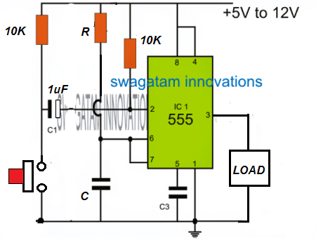
There are basically two methods through which the IC 555 can be used for generating pulse width modulation output. The first method is using only a single IC 555, and a few associated parts such as a diodes, a potentiometer and a capacitor. The second method is by using a standard monostable IC 555 configuration and using an external modulation signal.
IC 555 PWM using Diodes
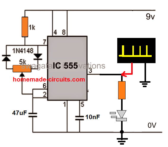
The first method is the simplest and effective, which uses the configuration as shown below:
Video Demonstration
The working of the above shown two diode IC 555 PWM circuit is quite simple. It's in fact a standard astable multivibrator design with the exception of an independent ON/OFF period control of the output.
As we know that the ON time of the IC 555 PWM circuit is decided by the time taken by its capacitor to charge at the 2/3rd Vcc level through pin#7 resistor, and the OFF time is determined by the discharging time of the capacitor below 1/3rd Vcc through the pin#7 itself.
In the above simple PWM circuit, these two parameters can be independently set or fixed through a potentiometer and through a couple of bifurcating diodes.
The left side diode which has its cathode connected with pin#7 separates the OFF time, while the right side diode which has its anode connected to pin#7 separates the ON time of the IC output.
When the potentiometer slider arm is more towards the left side diode, it causes the discharge time to decrease, due to lower resistance across the discharging path of the capacitor. This results in an increase in the ON time, and decrease in the OFF time of the IC PWM.
Conversely, when the pot slider is more towards the right side diode, it causes the ON time to decrease due to lowering of the resistance of the pot on the charging path of the capacitor. This results in an increase in the OFF period, and decrease in the ON periods of the IC output PWMs.
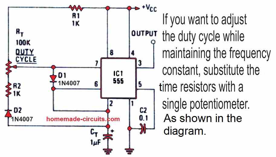
You can replace the timing resistors with a single potentiometer if you want to alter the duty cycle while keeping the frequency constant, as depicted in the following figure.
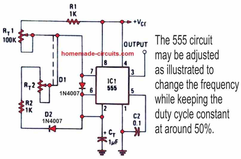
The 555 circuit may be adjusted as illustrated below to change the frequency while keeping the duty constant at around 50%.
2) IC 555 PWM using External Modulation
The second method is slightly complex than the above, and requires an external varying DC on pin#5 (control input) of the IC for implementing the proportionately varying pulse width at the IC output.
I have explained the following simple circuit configuration:
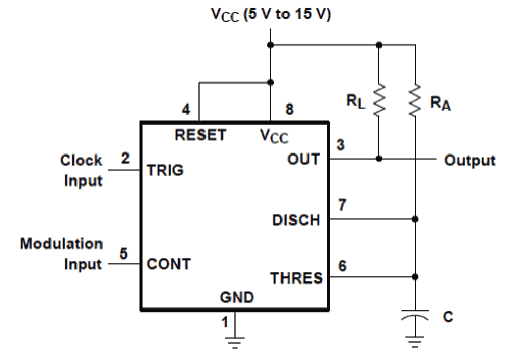
IC 555 Pinout
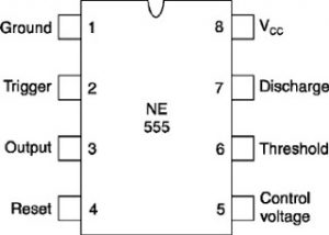
The diagram shows the IC 555 wired up in an easy monostable multivibrator mode. We know that in this mode the IC is able to generate a positive pulse at pin#3 in response to every single negative trigger at its pin#2.
The pulse at pin#3 sustains for some predetermined time period depending upon the values of Ra and C.We can also see the pin #2 and pin#5 assigned as clock and modulation inputs respectively.
The output is taken from the usual pin#3 of the chip.
In the above straightforward configuration the IC 555 is all set for generating the required PWM pulses, it just requires a square wave pulse or a clock input at its pin#2, which determines the output frequency, and a variable voltage input at pin#5 whose amplitude or the voltage level decides the pulse width dimensions at the output.
The pulses a pin#2 generates a correspondingly alternating triangle waves at pin#6/7 of the IC, whose width is determined by the RA and C timing components.
This triangle wave is compared with the instantaneous measure of voltage applied at pin#5 for dimensining the PWMs pulses at pin#3 output.
In simple words we just need to supply a train of pulses at pin #2 and a varying voltage at pin #5 for achieving the required PWM pulses at pin#3 of the IC.
The amplitude of the voltage at pin#5 will be directly responsible in making the output PWM pulses stronger or weaker, or simply thicker or thinner.
The modulation voltage can be a very low current signal, yet it would give the intended results.
For example suppose we apply a 50 Hz square wave at pin#2 and a constant 12V at pin#5, the result at the output will show PWMs with an RMS of 12V and frequency of 50Hz.
For reducing the RMS we just need to lower the voltage at pin#5. If we vary it the resultant will be a varying PWM with varying RMS values.
If this varying RMS is applied to a mosfet driver stage at the output, any load that is supported by the mosfet will also respond with correspondingly varying high and low results.
If a motor is connected to the mosfet, it will respond with varying speeds, a lamp with varying light intensities while an inverter with modified sine wave equivalents.
The Output Waveform
The above discussion can be witnessed and verified from the given waveform illustration below:
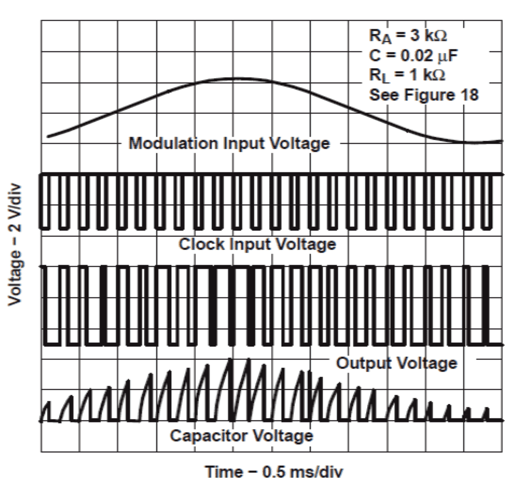
The topmost waveform represents the modulation voltage at pin#5, the bulge in the waveform represents the rising voltage and vice versa.
The second waveform represents the uniform clock pulse applied at pin#2. It's just for enabling the IC to switch at a certain frequency, without which the IC wouldn't be able to work as a PWM generator device.
The third waveform depicts the actual PWM generation at pin#3, we can see that the width of the pulses is directly proportional to the top modulation signal.
The pulse widths corresponding to the "bulge" can be seen as much wider and closely spaced which proportionately becomes thinner and sparse with the fall in the modulation voltage level.
The above concept can be very easily and effectively applied in power control applications as discussed earlier in the above article.
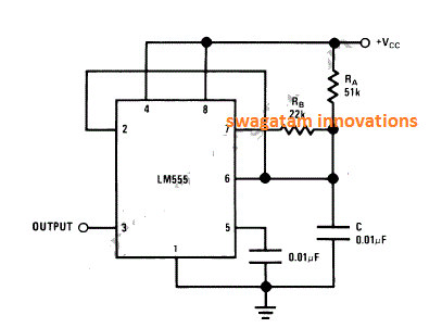
How to Generate a Fixed 50% Duty Cycle from a IC 555 Circuit
The following figure shows a simple configuration which will provide you with a fixed 50% duty cycle PWMs across its pin#3. The idea was presented in one of the IC 555 datasheets, and this design looks very interesting and useful for applications which need a simple and quick 50% fixed duty cycle generator stage.


Questions & Answers
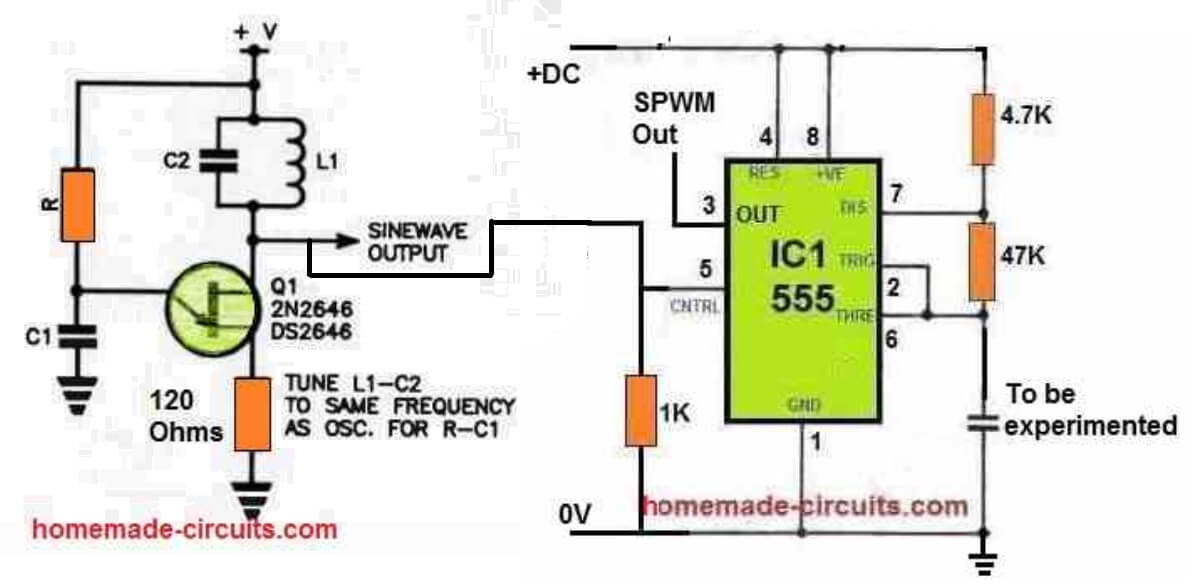
Hello, I am designing an SPWM circuit with the 555 IC for a pure sine wave inverter, modulating a 60Hz signal from my cell phone through pin 5 of the 555 to inject the SPWM signal into the MOSFET driver and then into the transformer
Yes, that’s fine, just apply the 60 Hz sine wave to pin#5 of your IC 555 astable circuit…and connect pin#3 to your mosfet driiver
Hello, good afternoon, Mr. Swagatam. Thank you for your quick response. I don’t think I explained it very well. I have to make a classic timer with Lm555… when the start button (pin 2) is pressed, it triggers… The timer starts, the load is activated… So far, so good. What I want is that if, due to some error, the single button remains pressed, I want the timer to continue working normally as usual, starting its time and then disconnecting… Regardless of whether the button remains pressed.
Thank you Carlos, in that case, you can try the following concept:
C3 = 0.01uF
R and C decides the output delay off timing…
Hello, good afternoon, Mr. Swagatam. Thank you for your quick response. Regarding the circuit, I found the solution, and it was very simple. As it is a timer that was to be activated by a PC817 optocoupler, I put a 100nf polyester capacitor in series on pin 1 and a 100k resistor in parallel with the capacitor. This ensures that it only activates on the first edge and then turns off even if the signal is still present… To reset the timer, the signal must be released or removed. In other words, if at any time there is a fault and the push button sticks, the LM555 will still perform its function.
Thanks Carlos, ….sounds great!! Glad you could solve the problem so quickly…
Hello, good afternoon, Mr. Swagatam. I would like to ask for your help. I need to make a timer with Lm555, but with the particularity that the time continues to run even if the button is pressed.
Hello good afternoon, Mr. Carlos,
Which button are you referring to, and how do you want the timer to function, please provide detailed description then I will try to figure it out…
Hello good afternoon Mr. Swagatam. In this opportunity I am bothering you to ask you if you can design an auto variable frequency generator circuit from about 10khz to about 26 kHz with an amplitude of 3.3v to 5v. I want it to simulate the inductive pressure switch of the washing machines, that way I can see how the electronic board behaves and therefore know if the problem is the board or the pressure switch. Thank you very much for your time.
No problem Carlos, you can try one of the designs explained in the following article. So if you feed a sine wave, or triangle wave input to these circuits, the output will vary in frequency depending on the amplitude of the input feed:
https://www.homemade-circuits.com/voltage-to-frequency-converter-circuit/
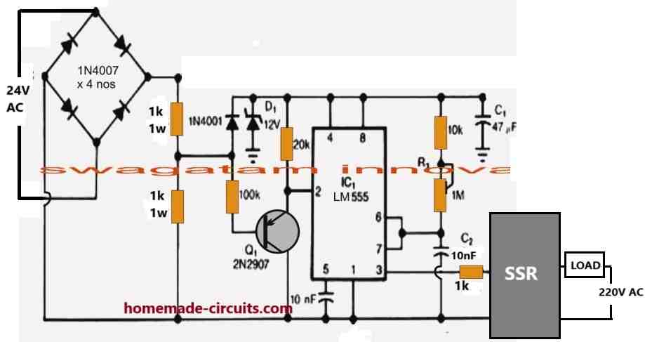
Hello good afternoon Mr. Swagatam. In this opportunity I would like to ask you if you have any circuit to simulate exactly the waveform and frequency of the 220vac 50 HZ mains maybe with a 555 or more simple … Thank you very much
Hello Carlos, I think the following design should be able to fulfil your requirement:
Thank you Swagatam, I think this looks like a good solution I will use a G3MB-202P SSR to control switching the AC to the motor.
A couple of questions:
1.I would like to power the transducer from the same circuit . It needs 5VDC where would be the best place to put a voltage reduction circuit to draw off the power for the transducer. Or would you recommend a separate power source for it ? Sorry I didn’t mention this earlier.
2. What is the 1M component connection below the 10k resistor to the top right of the 555? I haven’t seen a connection like that before.
Thank you for your help,
Alasdair
Sounds cool, Alasdair!
If your transducer requires very small current then you can derive the supply directly from the 555 12V supply itself, otherwise you might require a separate power supply for it, just make sure to make the ground line of the transducer supply common with the 555 supply.
The 1M is a preset resistor or a trimpot, which can be used to adjust the output PWM range and regulation of the SSR.
Sorry more details :
AC supply 230 -240 VAC
The motor draws max 1A
The transducer requires 5VDC
Regards,
Alasdair
Hi Swagatam , Your site is really interesting and helpful. I am looking to build an AC single phase motor control circuit based on the 555 using a triac, as in the second part of your article. I would like to control the PWM using the signal from a pressure transducer to control the output from the 555 to trigger the a triac to control the motor speed. The range of the output signal of the transducer is 0.5-4.5Vdc. I imagine the signal from the transducer will need conditioning with a instrumentation amplifier .
It would be my intention to power the DC side of the circuit at 12v using rectified AC from the source being switched by the PWM circuit. I have seen lots of control circuits for motors, fans, heaters but the primary control input method is most often a potentiometer rather than the input from a transducer. This sort of circuit must be quite common in the industrial process world but not do common in the hobby world. I understand that this can be done quite easily using a micro controller (arduino etc) but I would like to build it as an analogue control circuit as a learning experience.
Thank you,
Regards,
Alasdair
Thank you Alasdair,
For PWM AC load control, you can consider the following concept. The transducer output could be configured with pin#5 of the IC 555:
I have an application for a 555 timer circuit that will turn on a cob sound recorder. the time of the cob is 100 seconds and then must be re-triggered on. I thought an astable 555 multivibrator would do this. I had R1 equaling 102K, R2 equaling 205,022k and C1 470uF.
Essentially I want the 555 to turn the cob sound recorder on every 100 seconds. the sound recorder after playing shuts down and must be retriggered to play again. I made the 555 circuit using the above values but I could not get it to work. C2 was .1uF. The triggering did not work and I don’t know why. What 555 circuit should I be using?
thank you
When I do the math ,693(R1+2R2)C with the values you suggest I an T equalling 200 seconds not the 100s that I am looking for.
You suggested R1 = 10K, R2 = 295k and C= 480 uf
What am I doing wrong?
thank you
You want the recorder to be playing for 100 seconds, right? So it will be 100 seconds ON, and 99 seconds OFF.
If you do not want this,, then please let me know what should be the ON time of the recorder and the OFF time.
You can try the following values:
R1 = 10k
R2 = 295k
C1 = 480uF
Swagatham, Would it be possible to use the 555 to control the voltage output of a 220vac transformer? I am a little familiar with the concept etc, in that I know I would need a zero crossing circuit to trigger the the 555 and then the output would have to trigger a solid state relay. So how can I vary the pulse width with a potentiometer that would stay in phase with AC? Any suggestions would be greatly appreciated.
Hi Phil, If you wish to have a 555 PWM control with an SSR, you can use the first concept from the above article.
However, I would rather suggest you to implement a triac based AC control as explained in the following article:
https://www.homemade-circuits.com/simple-ceiling-fan-regulator-circuit/
Thank you for your help. Your explanations of how the 555 works is great! I’m sure I am in over my head trying to fix this old welder. It has a 50A solid state relay mounted on a suitable heatsink. The SSR has an input trigger of 3 – 30 vdc. The primary (220vac) is already connected to the SSR. The control board that that controls the signal going to the welder is bad (in part.) Other functions of the board work, just the HEAT (or power output) does not turn on the SSR. I have tried replacing components on the PC Brd (and replaced the SSR) but still does not work. The welder already has a potentiometer for control. I think it is 5k but I could change this. So what I am trying to do is come up with a fix for my old reliable welder. I have repaired this in the past by replacing the PC Brd but they are obsolete now and 3rd party replacements are out of my budget. I think I already know how to make the zero crossing circuit and I assume I could apply that to the trigger of the 555 to turn it on in phase with the 60 Hz AC. What I don’t know how to do is to get the potentiometer to adjust the output pulse of the 555 so as to control the pulse width when triggered by the zero crossing circuit. There is also a 24 vac power going to the original board. I am familiar with voltage regulators and rectifiers etc I may need, but it is this darn pulse width I am struggling width. It is taxing my 77 year old brain!
Hi, Thanks very much! Glad you liked the explanation.
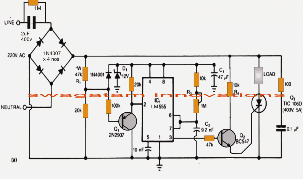
I think I already have a relevant circuit idea which closely matches your requirement.
Here’s a PWM zero crossing controlled 555 circuit which can be used with your SSR to control the load with PWM.
The BC547 and the SCR section can be replaced with your SSR configuration.
If you need I can redraw the circuit with an appropriate SSR included in the design.
Thank you very much for your quick response! Your designs all look amazing! I just wish I could remember what I learned 55 years ago about passive and active networks. I turned into a digital only kind of guy and still retain much of that. As for the circuit you suggested, I was hoping there might be a way to use the 24 vac transformer instead of connecting 220vac to the circuit design. Or I see that you have a 12v zenor to power the the 555. I think I could rectify the 24 vac and use a LM7812 to supply the 12v. What do you think? I hate to impose on your time and good nature so if I am asking more than I should – please accept my apology.
No problem at all. Please feel free to ask as many questions as you want, which will help us to share and gain more knowledge.
Yes, a 24 v ac supply from a transformer could be used to power the circuit and that would make the circuit much safer to handle. However the base potential divider might need to be modified so that a 12v or higher can be achieved from it to power the 555 stage. A 7812 might not be necessary, since the 12v zener would work without any issues with the low current voltage from the potential divider. Let me know your thoughts on this.
I believe I know what you mean.You are referring to voltage at the junction of the 47k and 20k resistors not being high enough? If that is the case I do not know how to recalculate those values.
Yes that’s correct. I have redesigned the circuit, which I think should do the job for you. You can find it in the following link:
Wow! Thank you so much! I will give this a try and let you know how it turns out. It looks to be exactly what I need.Maybe now I can get my garden cart welded and working again.
I doubt I could ever give you any technical advice on anything, but below you will find a couple of links where I have posted some instructional projects of my own.
I am currently working on another project for my wife who does stained glass and glass fusing. I am constructing a kiln from scratch.
Thanks again. Rare to find someone so willing and happy to help others.
hackster.io/pitg2000
instructables.com/member/pitg2000/
No problem Phil, I am always glad to help and all the best to you. Hope you succeed with the project.
Let me know if you run into any problems.
Swagatam. So I tried the circuit design and I do have some problems, and maybe I am causing them myself. First off, I did not have any 10nf capacitors and I substituted 1nf instead. I also did not have a 20k resistor and substituted a 22k. That having been done I was seeing a 1ms trigger occurring every 8ms.The trigger pulse width was variable as expected. The trigger went from ground to 8vdc, but when I connected it to the SSR it dropped down to 2vdc. Not really knowing exactly how to get the signal strength up above 3vdc required for the SSR, I played around with the series resistor going to the SSR. I managed to get the signal up to 5v. At this point the SSR was turning on and staying on but the voltage output did not vary any when I adjust the phase control.
I am really confused with this problem I am having because the original control board in the welder is sending almost an identical signal (albeit it goes from ground to 15vdc.) That signal does not turn the SSR on at all! I have tried 2 new Crydom SSRs.
This leads me to ask – don’t the SSRs have a zero crossing already built into them? If that is the case, what happens when you are already sending in a signal that is starting at zero volts? In the case of the original welder control board, it almost looks like the SSR gets turned on and back off at the same time!!
I realize that this is the holiday season so I am not expecting any prompt response. I am retired so every day is Saturday!
Have a nice holiday!
Thank you Phil,
It seems the monostable operation of the 555 IC during the zero crossings is happening correctly.
In that case the SSR must also switch the output at an identical rate. But as you say that is not happening.
Is your SSR built using MOSFETs or triac?
If it is MOSFET based then it should respond to the 1ms ON 8ms OFF time generated by the 555 output. However a triac based SSR may not respond to any PWM generated between the zero crossings and the peak of the AC wave cycles, because the triac will get latched and switch OFF only at the zero crossings, so the 1ms turn OFF after the zero crossing will never turn off the triac.
Regarding the voltage drop, SSRs are supposed to have high input impedance, so the voltage at their input must not drop, that’s strange?
SSRs do have zero crossing, but that is only to safeguard the load from switch ON transients.
However using the 555 circuit, it does not matter whether the SSR has a zero crossing or not because the 555 output will always switch ON the SSR only at the zero crossings.
So, if possible could you buy a MOSFFET based SSR? MOSFETs will not get latched and will respond and instantly turn OFF whenever the input is turned OFF at any point of the AC mains waveform.
Swagatham, so sorry for the late response and a BIG thank you for your repeated help. It appears as though the email address I have been using is not forwarding my messages. I will have to deal with that, so I will give you another email address in this reply.
I think you may be on to the real problem! I have both a cheap SSR I bought on Amazon (uxcell $14.00) and also a more expensive one (CRYDOM D2450). I dismantled the cheap one and you are correct. It has a BTA24 triac. I just looked on the datasheet for the D2450 and it has a SCR with zero crossing.
I was so sure that the original SSR in the welder was a D2450 but now I’m thinking I could be mistaken.
I don’t have to put a SSR back in the welder. I could use something else. There is already a fan cooled heatsink I could mount it on. Seems like the low power MOSFETs are inexpensive. I am not sure on 200v or 400v ones if that is the case. Can they be used in parallel to increase the current?
Actually I see looking through your website that you have an lesson on SSRs and MOSFETS. I need to study this in more detail.
No problem Phil, thank you for your reply!
Yes if the SSRs are built using SCR or Triac then they won’t be applicable for PWM switching.
MOSFETs will respond to PWM correctly, however single MOSFFETs might not work with an AC load.
In that case you may need a bidirectional MOSFET based SSR.
Let me know what you think about it?
My gosh! I am digging a hole deeper and deeper into this problem welder of mine. First let me say that I use to be the authorized repair center for this welder and replaced this circuit board and SSR literally hundreds of times. In the parts description for the welder it is called a “triac relay” and the part number is a 216-062-666. A couple of reputable dealers for welder parts sell the relay. They want $300 for it! They both show a picture of the relay. In the picture of one of them I see that it is a CRYDOM A2450 and can clearly see printed on the relay that the control input is 90 to 280vac. This can’t be the correct relay they are showing cause the control board for that part number (216-062-666) is the very same one I have in my welder and there is no way that it has any control voltage over 15vdc! Also, according to the CRYDOM data sheet it is SCR and not triac.
I don’t know whether this makes a difference or not, but the control output of the welder pc board is what I would call “negative logic.” The SSR has +15vdc on the pos+ and the signal goes to the -neg. Obviously the A2450 will not work, but assuming they meant to show the picture of the D2450 (which has a 3 to 30vdc control) can you see any scenario where either one of these would work.
Thanks Phil,
These SSRs are great for normal ON/OFF switching.
However since an SCR or Triac is involved, standard PWM control might not work correctly. Because SCRs and Triacs will latch up after each zero crossings, and will remain latched until the next zero crossing..
There’s one possible way where a PWM switching can be implemented to these devices, it is through PWM time proportional concept.
https://www.homemade-circuits.com/triac-phase-control-using-pwm-time/
A practical example of this concept can be seen in the first schematic of this article:
https://www.homemade-circuits.com/3-phase-induction-motor-speed/
Another thing to consider is, why not eliminate the SSR entirely and instead apply a triac phase control using a standard light dimmer principle?
https://www.homemade-circuits.com/simple-ceiling-fan-regulator-circuit/
Hi Swagatham, I need your help with a pwm circuit for an HHO generator. Can you show me a diagram for a circuit that converts 110 volts AC to DC, and then, let’s the operator change the pulse width through a potentiometer.
If possible please provide a list of components needed for building the circuit, and a detailed diagram of the circuit layout.
Many thanks for your assistance.
Hi Gary,
You can try the following design:
Hi Swagatam,
I’ve found this nice circuit (method 2) here, which I have also designed a few years ago for the voltage to pwm converter for my class D amplifier. I have some remarks from my experiences.
RL is not required for the CMOS versions of the 555 timer.
You can use one RA / C combination for multiple pwm converters. I have used one for both stereo channels of my class D amplifier.
The clock generator can be build up very similar to the converter circuit. Only the trigger pin (pin#2) must be also connected to the midpoint of the RA / C combination. And you have to set a reference voltage for 100% duty cycle to the modulation pin (pin#5).
If your application depend on linearity (as in the case of class D amplifiers) you need to substitute RA by a constant current source. I have used a current regulating diode (Siliconix CD056 in my case) as constant current source. So I have used a single CRD / C combination for the clock generator and both pwm converter circuits.
Thank Gunter,
I greatly appreciate your valuable feedback and information. Hope the other readers will find it useful.
Sir, in the first diagram where resistors are shown in orange color, connections on pin 7 (if I am not wrong) are looks wrong as variable resistor is looks short circuited.
I think R1 should not be connected to pin7 directly.
Hello Mohsin,
I cannot see anything wrong in the first circuit. The circuit is a tested design, you can see it in the video.
Thank you sir, pls I do not mean connecting the output pin 3 of spmw ICs
above directlyy to sg 3525 in the inverter. I will follow your directive to connect the pin to mosfet gates with individual diodes. What I mean sir is, is it safe or will it work if I use the first method of generating spmw explained in the above article in an sg3525 inverter. That’s an inverter that has sg3525 as it’s main IC Thanks.
Michael, As already mentioned in my previous comment, the above circuits will not generate SPWM, they will only generate uniformly divided PWMs.
Please read the article carefully to understand its working.
You can use the second concept for generating SPWM by connecting pin#4 50 Hz output from SG3525 with pin#2 of the IC555, and then feeding pin#5 of the IC 555 with 300 Hz triangle waves, which can be obtained from another IC 555 astable circuit from right across its timing capacitor.
Hello sir, pls under this explanation you did, which said by ” connecting the output pin 3 of the IC…….. pls there are many circuits here, is it under the first method which has a 555 IC with a pin 3 output connected to a red arrow and yellow stripes, also still under that circuit of the first method, there are two wires out tagged “9v” and “0v”, pls where do these wires go. Lastly still under this first method’s circuit, I want to use it in an sg3525 inverter, should I go on thanks.
Hello Michael, all the diagrams above will generate a pwm controlled output at pin3 of the ICs, so you can use any one of them. Connecting to SG3525 will not help to get sine wave output because the above pwms are not SPWMs, they can be used only to control the RMS of the inverter output. The 0 and 9V can be connected to the battery of the inverter.
Thanks sir for your Swift response, pls I want to enquire, can I use the 12v d.c. from a normal or advanced car alternator rotating at it’s normal or highest possible rpm to power a 2k watt or at least a 1k watt Inverter. That is the inverter will only be powered by the current from the alternator in place of a battery. If it’s feasible, like how long can that arrangement last with little or no harm to the inverter or the alternator itself. If there are pros, pls let me know also through your reply. Thanks, will be waiting for your reply. Merry Christmas to you and your people ❤️
Michael, an inverter just needs a DC supply to convert the DC into mains AC, it doesn’t matter from where the DC is coming. If you can convert the alternator AC to Dc to feed the inverter then the inverter will do its job normally, as it would do with any battery. However to operate a 1000 watt load the alternator output power will need to be much above this value.