In this post I have explained the method of designing buck converter circuits by calculating all the required parameters, in order to ensure an optimal performance from these devices.
We take the example of IC 555 buck converter typologies, and try to understand the optimizing techniques through equations and manual adjustments, for achieving the most optimal output response from these converter designs.
You may want to summarize the details from the following articles, before embarking on the present article which deals with the inductor designing methods.
How to Design: Basic Buck Converter Equations
The crucial specifications needed to design a buck converter are as given below::
Duty Cycle Calculation
Now, the crucial element required for calculating the inductor, is the duty cycle. We can use the following formula for calculating the duty cycle:
D = Vout / Vin
The next crucial thing for calculating the buck inductor is the Ripple Current, which can be calculated in the following manner:
Target Inductor Ripple Current (ΔIL): As a rule of thumb, you can choose 10% of output current.
Calculating the Buck Inductor
Now, finally we can calculate the buck inductor, using the following formula:
L = (VOUT × (1 - D)) / (ΔIL × fs)
Next, we need to calculate the output filter capacitor, which requires the Ripple Voltage ΔVOUT
As a rule of thumb, we can take the Voltage Ripple (ΔVout) as 1% of output voltage.
Now, we can calculate the value of the output capacitor in the following manner:
Output Filter Capacitance Calculation for Buck Converter:
COUT = ΔIL / (8 × fs × ΔVout)
When we design a buck converter, the output ripple voltage ΔVout is mainly affected by two things, the inductor ripple current ΔIL and the output capacitor Cout.
You might be wondering where that factor of 8 came from.
It appears when we use an estimate to connect the peak-to-peak ripple voltage, peak-to-peak ripple current, and capacitance value. We assume that the ripple waveform is shaped like a triangle, which is a popular method in these computations.
So, in simple terms, number 8 is simply the result of reducing our arithmetic while preserving everything relevant to how the output ripple acts in continuous conduction mode (CCM).
Choose an output capacitor rated at least 250 μF with a voltage rating above 100V and low ESR.
Diode Selection
Reverse Voltage: Greater than input voltage with a safety margin.
Average Current Rating: Should be 1.5 times higher than the output current.
Switch (MOSFET) Selection
For the MOSFET to work efficiently, make sure to consider the following parameters:
Voltage Rating VDS of the MOSFET should be higher than the input voltage, typically 1.2-1.5 times.
Current Rating ID of he MOSFET must be selected so that the MOSFET can handle peak current.
The RDS(on) value must be selected to be minimum to reduce conduction losses.
By appropriately adjusting any one of the above parameters it becomes possible to tailor the output voltage from the converter. This adjustment could be implemented manually or automatically through a self adjusting PWM circuit.
Although the above formulas clearly explain how to optimize the output voltage from a buck converter, we still do not know how the inductor can be built for getting an optimal response in these circuits.
Solving an Example Buck Converter Design
Let's say we want to design a buck converter with 60V input and 12V output with 5 Amp current, let's calculate the above discussed parameters.
Given Specifications
- Input Voltage (Vin): 60V
- Output Voltage (Vout): 12V
- Output Current (Iout): 5A
- Switching Frequency (fs): Let us assume 100 kHz (a common choice for this power range)
Duty Cycle Calculation
- Formula: Duty Cycle (D) = Vout / Vin
- Calculation: D = 12 / 60 = 0.2
- Result: Duty Cycle (D) = 20%
Inductor Selection
- Target Inductor Ripple Current (ΔIL): Assume 10% of output current, so:
- ΔIL = 0.1 × Iout = 0.1 × 5 = 0.5 A
- Inductance Calculation:
- Formula:
- L = (Vout × (1 - D)) / (ΔIL × fs)
- Calculation:
- L = (12 × (1 - 0.2)) / (0.5 × 100,000) = (12 × 0.8) / 50,000 = 9.6 / 50,000 = 0.000192 H
- Result:
- Inductance (L) = 192 μH
- Choose an inductor with a value close to 192 μH, rated for at least 5A current.
Output Capacitor Selection
- Target Voltage Ripple (ΔVout): Let us assume 1% of output voltage, so:
- ΔVout = 0.01 × Vout = 0.01 × 12 = 0.12 V
- Output Capacitance Calculation:
- Formula:
- Cout = ΔIL / (8 × fs × ΔVout)
- Calculation:
- Cout = 0.5 / (8 × 100,000 × 0.12) = 0.5 / 9600 = 52.08 μF
- Result:
- Output Capacitance (Cout) = 52 μF
- Choose an output capacitor rated at least 52 μF with a voltage rating above 12V, and low ESR for handling ripple current.
Diode Selection
- Reverse Voltage: Greater than input voltage (60V), with a safety margin.
- Average Current Rating: Should be higher than the output current, so choose a diode rated for at least 5A (ideally 6A for reliability).
Switch (MOSFET) Selection
- Voltage Rating: Higher than the input voltage, typically 1.2 to 1.5 times Vin (60V), so choose a MOSFET rated for at least 80-90V.
- Current Rating: Should be able to handle peak current, so at least 8A (10A is recommended for safety).
- Low RDS(on): To reduce conduction losses and increase efficiency.
Final Results for our example 60V to 12V Buck Converter Design
- Duty Cycle: 20%
- Inductor: 192 μH
- Output Capacitor: 52 μF (voltage rating > 15V)
- Diode: Reverse voltage > 60V, current rating > 5A
- MOSFET: Voltage rating > 80V, current rating > 5A, low RDS(on)
Using Practical Trial and Error Method
You may find many elaborate and researched formulas for settling this issue, however no new hobbyist or any electronic enthusiast would be interested to actually struggle with these complex formulas for the required values, which could actually have more possibility of providing erroneous results due to their complexities.
The better and more effective idea is to "calculate" the inductor value with an experimental set up and through some practical trial and error process as explained in the following paragraphs.
The inductor L may be initially made arbitrarily.
The rule of the thumb is to use the number of turns slightly higher than the supply voltage, therefore if the supply voltage is 12V, the number of turns could be around 15 turns.
- It must be wound over a suitable ferrite core, that could be a ferrite ring or a ferrite rod, or over an EE core assembly.
- The thickness of the wire is determined by the amp requirement which initially won't be a relevant parameter, therefore any relatively thin copper enameled wire would work, may be around 25 SWG.
- Later on as per the current specs of the intended design, more number of wires could be added in parallel to the inductor while winding it in order to make it compatible with the specified ampere rating.
- The diameter of the inductor will depend on the frequency, higher frequency would allow smaller diameters and vice versa. To be more precise, the inductance offered by the inductor becomes higher as frequency is increased, therefore this parameter will need to be confirmed through a separate test using the same IC 555 set up.
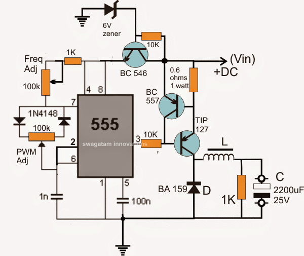
Basic Circuit Diagram Buck Converter
In-Depth Buck Converter Designing Details
In this section I have explained the various parameters required for designing a correct buck converter inductor, such that the required output is able to achieve maximum efficiency.
In our previous post I explained the basics of buck converters and realized the important aspect regarding the transistor's ON time with respect to the periodic time of the PWM which essentially determines the output voltage of the buck converter.
In this post we'll go a little deeper and try to evaluate the relationship between the input voltage, switching time of the transistor, output voltage and the current of the buck inductor, and regarding how to optimize these while designing a buck inductor.
Buck Converter Specifications
Let's first understand the various parameters involved with a buck converter:
Peak inductor current, ( ipk) = It's the maximum amount of current that an inductor can store before getting saturated. Here the term "saturated" means a situation where the transistor switching time is so long that it continues to be ON even after the inductor has crossed its maximum or peak current storing capacity. This is an undesirable situation and must be avoided.
Minimum Inductor Current, (io) = It's the minimum amount of current that may be allowed for the inductor to reach while the inductor is discharging by releasing its stored energy in the form of back EMF.
Meaning, in the process when the transistor is switched OFF, the inductor discharges its stored energy to the load and in the course its stored current drops exponentially towards zero, however before it reaches zero the transistor may be supposed to switch ON again, and this point where the transistor may switch ON again is termed as the minimum inductor current.
The above condition is also called the continuous mode for a buck converter design.
If the transistor does not switch ON back before the inductor current has dropped to zero, then the situation may be referred to as the discontinuous mode, which is an undesirable way to operate a buck converter and may lead to an inefficient working of the system.
Ripple Current, (Δi = ipk - io) = As may be seen from the adjoining formula, the ripple Δi is the difference between the peak current and minimum current induced in the buck inductor.
A filter capacitor at the output of the buck converter will normally stabilize this ripple current and help to make it relatively constant.
Duty Cycle, (D = Ton /T) = The duty cycle is calculated by dividing the ON time of the transistor by the periodic time.
Periodic time is the total time taken by one PWM cycle to complete, that is the ON time + OFF time of one PWM fed to the transistor.
ON time of the Transistor ( Ton = D/f) = The ON time of the PWM or the "switch ON" time of the transistor may be achieved by dividing the duty cycle by the frequency.
Average output current or the load current, (iave = Δi / 2 = iload ) = It's obtained by dividing ripple current by 2. This value is the average of the peak current and the minimum current that may be available across the load of a buck converter output.
RMS value of Triangle wave irms = √{io2 + (Δi)2 / 12} = This expression provides us the RMS or the root mean square value of all or any triangle wave component that may be associated with a buck converter.
OK, so the above were the various parameters and expressions essentially involved with a buck converter which could be utilized while calculating a buck inductor.
Now I have explained how the voltage and current may be related with a buck inductor and how these may be determined correctly, from the following explained data:
Remember here we are assuming the switching of the transistor to be in the continuous mode, that is the transistor always switches ON before the inductor is able to discharge its stored EMF completely and become empty.
This is actually done by appropriately dimensioning the ON time of the transistor or the PWM duty cycle with regard to the inductor capacity (number of turns).
V and I Relationship
The relationship between voltage and current within a buck inductor may be put down as:
V = L di/dt
or
i = 1/L 0ʃtVdt + io
The above formula may be used for calculating the buck output current and it holds good when the PWM is in the form of an exponentially rising and decaying wave, or may be a triangle wave.
However if the PWM is in the form of rectangular waveform or pulses, the above formula can be written as:
i = (Vt/L) + io
Here Vt is the voltage across the winding multiplied by the time for which it's sustained (in micro-secs)
This formula becomes important while calculating the inductance value L for a buck inductor.
The above expression reveals that the current output from a buck inductor is in the form of a linear ramp, or wide triangle waves, when the PWM is in the form of triangular waves.
Now let's see how one may determine the peak current within a buck inductor, the formula for this is:
ipk = (Vin – Vtrans – Vout)Ton / L + io
The above expression provides us the peak current while the transistor is switched ON and as the current inside the inductor builds up linearly (within its saturation range*)
Calculating Peak Current
Therefore the above expression can be used for calculating the peak current build-up inside a buck inductor while the transistor is in the switch ON phase.
If the expression io is shifted to the LHS we get:
ipk - io = (Vin – Vtrans – Vout)Ton / L
Here Vtrans refers to the voltage drop across the transistor's collector/emitter
Recall that the ripple current is also given by Δi = ipk - io, therefore substituting this in the above formula we get:
Δi = (Vin – Vtrans – Vout)Ton / L ------------------------------------- Eq#1
Now let's see the expression for acquiring the current within the inductor during the switch-OFF period of the transistor, it may be determined with the help of the following equation:
io = ipk - (Vout – VD)Toff / L
Again, by substituting ipk - io by Δi in the above expression we get:
Δi = (Vout – VD)Toff / L ------------------------------------- Eq#2
The Eq#1 and Eq#2 can be used for determining the ripple current values while the transistor is supplying current to the inductor, that is during it's ON time..... and while the inductor is draining the stored current through the load during the transistor switch OFF periods.
In the above discussion we successfully derived the equation for determining the current (amp) factor in a buck inductor.
Determining Voltage
Now let's try to find a expression which may help us to determine the voltage factor in a buck inductor.
Since the Δi is common in both Eq#1 and Eq#2, we can equate the terms with each other to get:
(Vin – Vtrans – Vout)Ton / L = (Vout – VD)Toff / L
VinTon – Vtrans – Vout = VoutToff – VDToff
VinTon – Vtrans – VoutTon = VoutToff - VDToff
VoutTon + VoutToff = VDToff + VinTon – VtransTon
Vout = (VDToff + VinTon – VtransTon) / T
Replacing the Ton/T expressions by duty cycle D in the above expression, we get
Vout = (Vin – Vtrans)D + VD(1 – D)
Processing the above equation further we get:
Vout + VD = (Vin – Vtrans + VD)D
or
D = Vout - VD / (Vin – Vtrans – VD)
Here VD refers to the voltage drop across the diode.
Calculating Step Down Voltage
If we ignore the voltage drops across the transistor and the diode (since these can be extremely trivial compared to the input voltage), we can trim down the above expression as given below:
Vout = DVin
The above final equation can be used for calculating the step down voltage that may be intended from a particular inductor while designing a buck converter circuit.

Questions & Answers
Good, the 555 buck converter design is working, as the voltage decreases there was no current gain, at 80khz for 24v battery 32v voltage input.
please sir, any help?
Dan, the above calculations are correct, so without checking your circuit practically it is difficult to judge the fault….
please what is the function of bc546 and the 6v zener network in the above circuit.
BC546 is a voltage regulator circuit to supply a constant low voltage to 555 circuit.
Thanks sir, please function of bc 557 and 1watts 0.6ohms.
Those parts are configured as a current limiter to safeguard the main buck transistor from overcurrent.
Grateful sir, Wow, I like this circuit. Please how can I use this 555 buck converter circuit for My requirements AC 150v to 24vDc.
Thanks for always being supportive.
Thanks Dan, yes you can use 555 for your application. Since you are using an AC, a flyback type converter would be more suitable. In that case you may have to take the help of the following software:
https://www.homemade-circuits.com/smps-transformer-calculator-2/
please what is the efficiency of 555 buck converter?
It will depend on the the inductor design.
please what is the best switching frequency for highest efficiency I can use?
50 kHz to 100 kHz
Sir, assuming I get the perfect inductor, please what will the efficiency be for 555 buck converter?
Dan, Efficiency can be upto 90%
Thanks sir, if 555 can be used, I would prefer it, so please kindly assist with elaborate guide to achieving this buck converter?
please what are the modifications that will be needed? I appreciate, sir.
Dan, you can take the help of the following software to design the circuit:
https://www.homemade-circuits.com/buck-converter-calculator/
https://www.homemade-circuits.com/ic-555-timer-astable-circuit-calculator/
Just make sure to supply the 555 positive from a separate 12V DC supply…
Hi Swagatam
we discussed earlier in post 0 to 100 volt smps
you suggest i need a buck converter to get efficient 0 to 100 volt at 10 amps
.
then you give me link of this post
.
i see your circuit diagram
thats not full feel my requirement
.
my question is…..
i have bunch of 48 to 72 volt input
12 volt 20 amps output (use in electric rikshaw to power its light and indicator)
.
they all have uc 3842,45 ic
.
my question is….
when i try to modify its feedback
result is not like my expectations
.
when i short tl431 referance pin to output
minimum voltage i get 6 volt
.
i also cant understand its feedback section
.
this converter use high end side mosfet driving
.
uc 3845 pin number 2 shorted to pin 5
and opto coupler atteched to pin 1 and 2
real question is when feedback pin is 2
then why use pin number 1 ?
thanks for your regular help
Hi Naresh,
We have discussed this in the previous comments, where I suggested you to build a buck converter instead of depending on the feedback network, and you agreed to try the buck converter method, because solving the feedback network will require me to check your circuit practically, which is not possible.
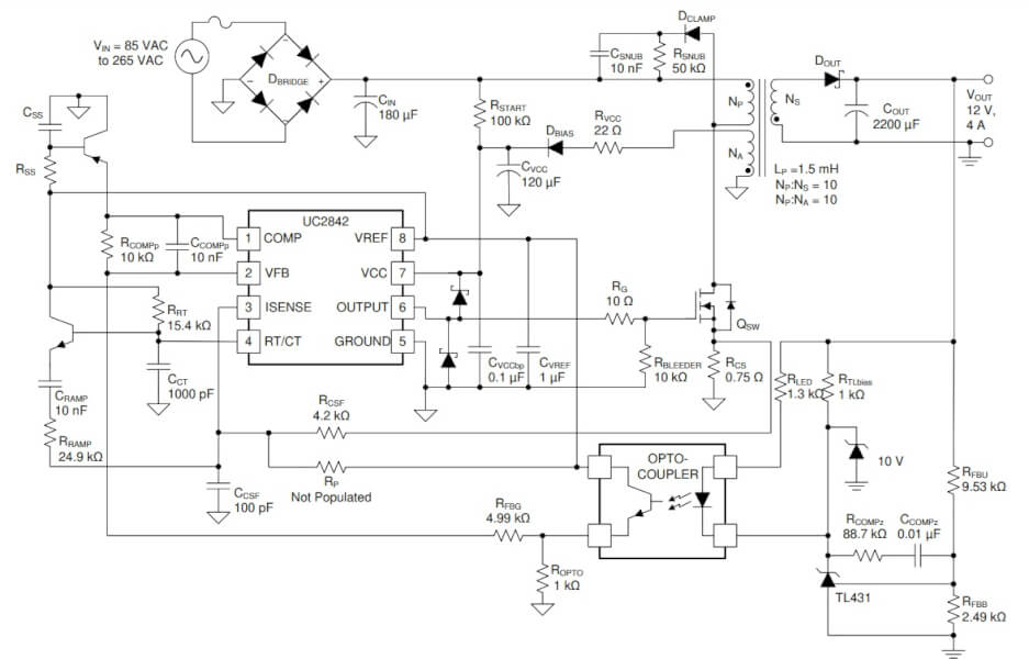
Yes, pin#2 must be used as the feedback. Please refer to the following diagram:
thank brother
i discuss buck converter yet
.
i have many 48 to 72 volt input 12 volt 20 amp output buck converter
.
but i can’t modify its feedback to control output voltage 1 to 72 volt
.
when i get sucses then i want to modify it 0 to 100 volt buck converter
Yes, I understand, if you provide me with the circuit diagram of the buck converter or the IC number, then I may try to figure out the feedback working.
how can i share circuit diagram??
there is no option to share jpeg image ?
ic use in buck converter uc3845
you can send it to my email ID
homemadecircuits
@gmail.com
I will check it.
Hi Mr Swagatam;
when buck converter value is 82V to 25V or low, is it possible to use 1N4007 or any fast diodes instead of the 4148 diodes?
Hi Suat,
Yes, you can use a fast diode like FR107 or BA159 instead of 1N4148, but 1N4007 might not be suitable.
thanks Mr. Swagatam;
so then the pending point for me that can 555 handle the 82V directly or not?
Suat, 555 cannot take more than 15V, so 82V is way too high.
Hi Mr Swagatam;
Is it possible to reduce 82V DC to 15V DC by using the above buck or any other converter circuit?
Hi Suat,
Yes it may be possible if the coil, the PWM and the frequency are correctly optimized.
thanks for the support. So should I change the base resistor value and add any resistor before the transistor due to maximum rating of the bc546 and please advice if 555 can tolerate the input 82V.
Hi Suat, BC546 might not be suitable for handling 80v…you can use TIP31C instead, which is rated at 100v…
also initially you can remove the bc557 current limiting stage, and check the results without it.
Hi Sir
I need a buck circuit with wide input voltage from 10 to 120 volts and output of 14volts 10 amps. Request your help with the circuit and Inductor value and capacitor value and switching frequency
Hi Sanjay,
120V is too high, I have a circuit which can handle a maximum of 40 V only.
PWM Solar Battery Charger Circuit
Dear Mr Swagatam.If I want to increase the amperage (to like 10amps) of this boost converter what do i need to do?
Dear Bello, current can be increased by increasing the wire thickness or density, but first verify the proper working of the basic design, only then the upgrade can be implemented.
Please what’s the function of bc546 and the zener 6v.thanks
it is configured as a voltage regulator, for stabilizing the supply to the IC at 6V fixed
Hi Swag, between the bc546 and zener, and 7806 voltage regulator, which is better between the two. Thanks sir
Hi Tolu, 7806 is better but its input voltage is limited to maximum 32V.
I tried this ic 555 buck converter circuit but the the Vout just had 0.25v diff without no variation despite turning the pwm preset. The gate and emitter voltage are thesame. What can I do .thanks
that’s not possible unless you have done some mistake in your connections, I will try to upload a working video of it soon…
Hello, I changed the tip in the Buck converter to p-channel MOSFET, there was wide variation in the voltage as against the tip with no much difference why varying the pots. Why the transistor not showing difference as to the MOSFET in reference to the Vin.
If your IC works correctly and if you are able to vary the PWM at pin#3 then definitely you will be able to see a varying output through the buck.
did you test the PWM with an oscilloscope? test it with a scope that will prove whether your circuit is working correctly or not.
Thanks Swag, the buck converter worked. But its configuration is different from that one in simple mppt circuit which I tried but not working. Like I said earlier, the p1 resistance variation is range of 0-236ohms. Any advice to that.
Did you check the procedures which I suggested you earlier by isolating the various stages? disconnect the IC1, IC2 the opamp and the solar panel from each other, confirm the stages separately
I did it, anything less than 10v the ic2 didn’t drive the motor.
pin#5 of IC 2 is already at 2/3rd Vcc internally, and will able to produce 75% speed on the motor when nothing is applied at pin#5, reducing this level to lower values will proportionately reduce the motor speed…it is a standard IC 555 pwm circuit
you can understand it better by referring to this post
https://www.homemade-circuits.com/constant-torque-dc-motor-speed/
Please I need a simple dc-dc converter circuit to step down 48v to 12v for my inverter oscillator stage.
search for buck converter in this website, you can use it for the purpose…
I tried this ic 555 buck converter circuit but the the Vout just had 0.25v diff without no variation despite turning the pwm preset. The gate and emitter voltage are thesame. What can I do .thanks