• Skip to main content
  • Skip to primary sidebar

Homemade Circuit Projects

Need circuit help? Post them in the comments! I've answered over 50,000!

Blog | Categories | About | Hire Me | Contact | Calculators-online
You are here: Home / Electronics Theory / How Load Conducts in Half-Bridge Driver Circuits like IR2184 or IR2110

How Load Conducts in Half-Bridge Driver Circuits like IR2184 or IR2110

Last Updated on September 10, 2026 by Swagatam 8 Comments

Many folks, especially beginners, they get fully confused when they try to use a half-bridge driver circuits using ICs like IR2184 or IR2110. They look at the datasheet diagram and start thinking, “Bro, how the load will conduct? The MOSFETs are switching one by one so how the current will pass through the load? Looks like the circuit is incomplete…”

Table of Contents
  • First Let us Understand the Basic Half-Bridge MOSFET Section
  • Then Comes the Confusion from Datasheet Diagram
  • Correct Way to Connect Load in Half-Bridge
    • Load must be between VS and GND
  • So How Does the Load Conduct?
    • When High-Side MOSFET is ON:
    • When Low-Side MOSFET is ON:
    • When you do PWM on high-side:
  • If You Connect Load Wrongly
  • Final Conclusion

But actually the datasheet is not wrong — it is just not fully showing the load connection in clear way. So here in this article we will try to fully break this thing down and explain — how exactly the load gets power and how it conducts in a half-bridge circuit.

First Let us Understand the Basic Half-Bridge MOSFET Section

We take two N-channel MOSFETs, and connect them like this:
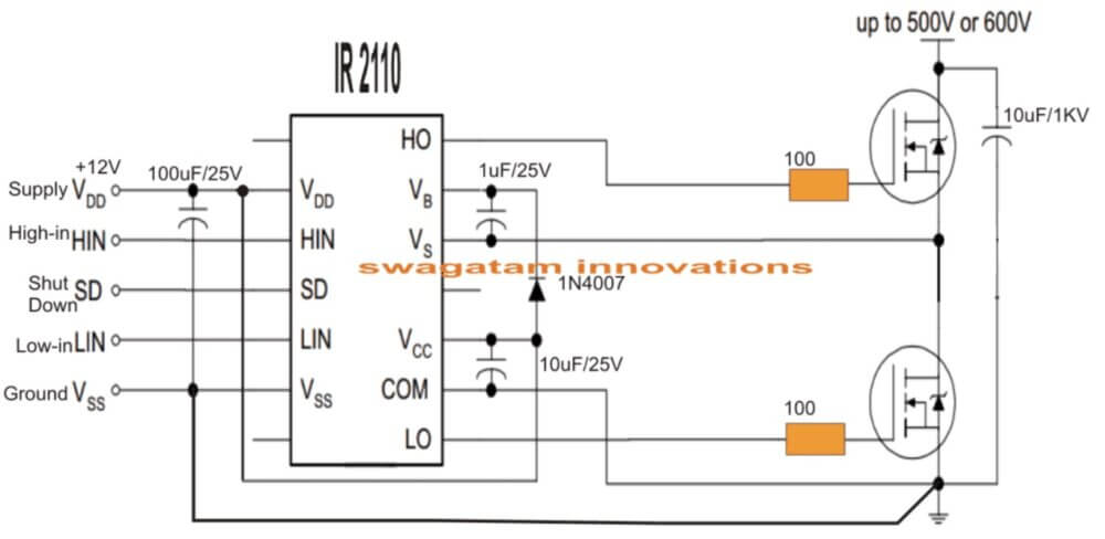
Note: Please make sure to replace the 1N4007 diode with a UF4007 or any other fast diode like FR107 or BA159

  • Top MOSFET (called high-side) has:
    • Drain = connected to high voltage DC bus (like 310V or 600V DC)
    • Source = connected to VS node (midpoint node)
  • Bottom MOSFET (called low-side) has:
    • Drain = connected to same VS node
    • Source = connected to GND

So basically both MOSFETs are connected in series, and the middle point between them is called VS. This VS point is super important — this is where we take output to the load.

Then Comes the Confusion from Datasheet Diagram

Now if we see the official diagram from IR2184 or IR2110 datasheet, we will find that the “TO LOAD” point is connected to the VS node, which is correct.
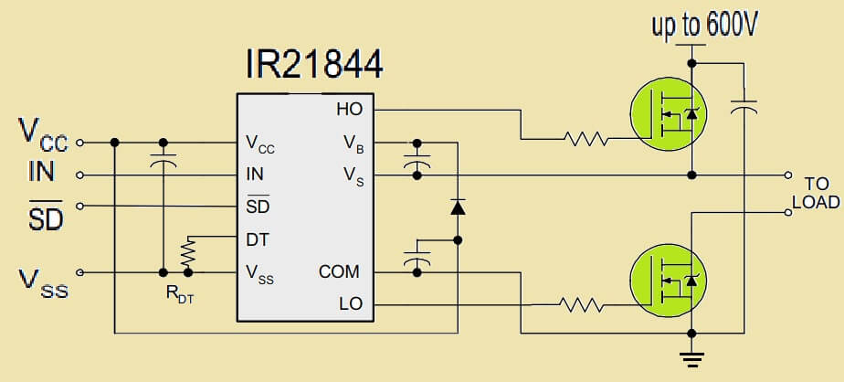
But then it shows another “TO LOAD” terminal coming out from somewhere around low-side FET. But the datasheet does not show where this second terminal is going. That is what creates full confusion.

People start thinking:

“Bro, shall we connect the load between VS and drain of low-side FET? Then when high side is ON and low side is OFF, how will current complete the path?”

Yes that question is valid. And if we do not know how the circuit is meant to be wired in real life, we will get confused.

Correct Way to Connect Load in Half-Bridge

The real, proper way to connect the load (like a bulb or motor) is this:
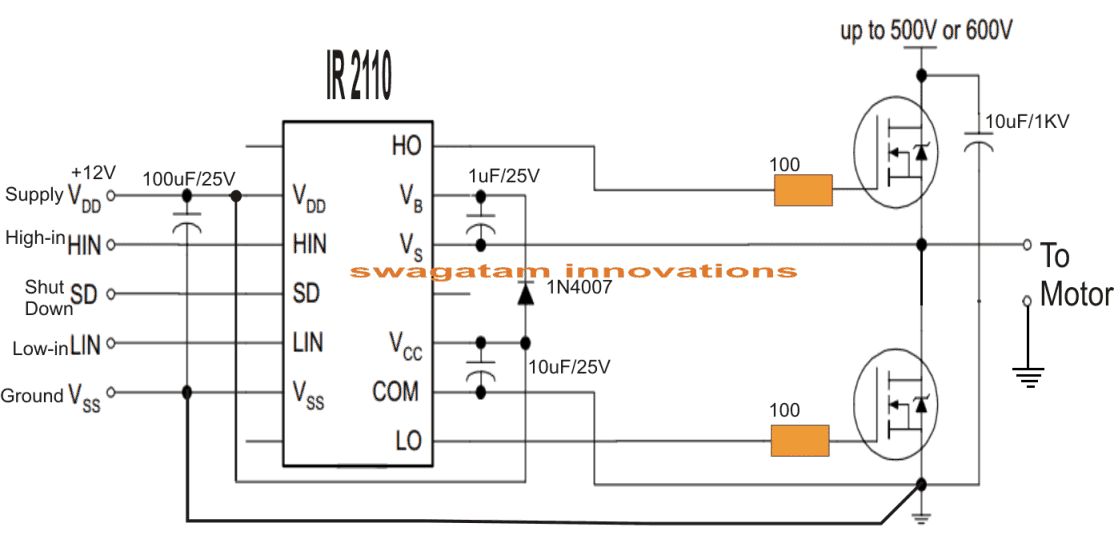
Note: Please make sure to replace the 1N4007 diode with a UF4007 or any other fast diode like FR107 or BA159

  • One terminal of the load goes to the VS node which is the middle point between both MOSFETs.
  • The other terminal of the load must go to system GND.

That is all. This is the correct method.

Load must be between VS and GND

Do not connect the load between VS and drain of low-side FET, that will never work properly.

So How Does the Load Conduct?

Now let us see what happens when the MOSFETs switch one by one.

When High-Side MOSFET is ON:

  • Current flows like this:
    +Vbus > High-side FET > VS node > Load > GND
  • So full supply voltage comes across load
  • Load conducts, bulb glows

When Low-Side MOSFET is ON:

  • VS node is now pulled to ground.
  • Load sees 0V across it (both ends at GND).
  • No current flows.
  • Load stays OFF.

When you do PWM on high-side:

  • Load gets pulsed voltage at PWM frequency.
  • Load operates with average power based on duty cycle
  • Motor can be speed controlled etc.

This is how half-bridge actually works.

If You Connect Load Wrongly

Suppose you make the mistake of connecting one terminal of the load to junction of High side MOSFET Source and the VS, and the other terminal of the load to drain of low-side FET. Then:

  • When High-side MOSFET is ON then Load gets the full DC supply which is floating on its one terminal, but the load cannot operate because the low-side MOSFET is OFF, so circuit cannot complete.
  • When low-side FET turns ON, the High-side MOSFET turns OFF, and then the other terminal of the load is pulled to ground, again the load cannot operate because the DC supply is not there (high-side turned OFF)
  • That means when the MOSFETs switch alternately, both terminals of load are floating or shorted — so no real voltage appears across load
  • Load does not get proper conduction path.
  • Sometimes it may even damage FET or cause weird results.

So this load configuration is wrong and should never be used.

So, in our recommended, correct configuration the load (like a bulb or motor) is just sitting between the junction of High-side MOSFET source and VS, and the supply DC GND.

Whenever the high-side FET turns ON, the High-side MOSFET Source and VS junction becomes high (like 310V), and so the load gets voltage across it, so it gets powered and operates.

When high-side MOSFET is OFF and low-side is ON, then VS becomes 0V, so both ends of load now get 0V, so no conduction happens, load remains turned OFF.

This simple logic gives you pulsed DC to the load, controlled by your gate PWM.

Final Conclusion

  • The datasheet diagram is not wrong — but it is incomplete. It does not show where the second load wire goes.
  • You must manually connect the second load wire to GND.
  • Load must always be between VS node and ground.
  • Do not connect load between VS and any other random drain or point — it will not work.
  • This is how half-bridge drivers like IR2184 or IR2110 properly operate the load.

So guys, next time when you use a half-bridge MOSFET driver, just remember this:

“Load must be connected between the junction of High-side MOSFET + VS and DC GND - that is all. High-side MOSFET ON means load gets full DC supply, low-side MOSFET ON means load goes OFF.”

You'll also like:

  • inverterHow an Inverter Functions, How to Repair Inverters – General Tips
  • Understanding Bipolar Junction Transistors (BJTs)
  • Ohm’s Law/Kirchhoff’s Law using Linear First-Order Differential Equations
  • piezotransducerelementUnderstanding and Using a Piezo Transducer

Filed Under: Electronics Theory, Inverter Circuits Tagged With: Bridge, Circuits, Conducts, Driver, Half, Load

About Swagatam

I am an electronics engineer and doing practical hands-on work from more than 15 years now. Building real circuits, testing them and also making PCB layouts by myself. I really love doing all these things like inventing something new, designing electronics and also helping other people like hobby guys who want to make their own cool circuits at home.

And that is the main reason why I started this website homemade-circuits.com, to share different types of circuit ideas..

If you are having any kind of doubt or question related to circuits then just write down your question in the comment box below, I am like always checking, so I guarantee I will reply you for sure!

Previous Post: « IC IR2184, IR21844 Half-Bridge Driver Circuit Diagram, Datasheet, Working
Next Post: Do We Need a Freewheeling Diode Across the Inductor in Boost Converter? »

Reader Interactions

Questions & Answers

Total Posts: 8
Newest Oldest
Peter
March 2, 2026 • 7 months ago #201981

Can you use Mosfets to switch or Isolate my solar PV array +- 400Vdc @ 18 Amps?

Reply
SwagatamAdmin
March 2, 2026 • 7 months ago #201991

Yes, we can do that!

Reply
navid salmani
June 7, 2026 • 4 months ago #208045

hi master.
my h bridge have 4 mosfet and work in 20khz.
but I have a problem in gnd and com and vs in ir 2110.
will be damage.

Reply
SwagatamAdmin
June 8, 2026 • 4 months ago #208064

Hi Navid, please see the IR2110 diagram shown in the above article, Vss and ground are common….and Vcc is the +12V DC input

Reply
Emil Stefanov
September 12, 2026 • 3 weeks ago #212546

Hi Swagatam, can I use IR2110 to drive simultaneously the 2 MOSFETS as is needed is needed for a two-switch forward converter? Thank you in advance for your advice and help! Emil

Reply
SwagatamAdmin
September 13, 2026 • 3 weeks ago #212551

Hi Emil, yes, IR2110 can be used for a two-switch forward converter, and in this case both MOSFETs can be driven ON and OFF at the same time.
For the control, the same PWM signal can be applied to both HIN and LIN, so HO and LO turn ON together and turn OFF together. This is what is required for the two-switch forward topology. You should not use complementary PWM for HIN and LIN as you would in a normal half-bridge.

But rememeber, the bootstrap supply needs enough OFF time to recharge properly, so the PWM duty cycle should normally be kept below about 50% in a two-switch forward converter. The transformer reset action itself also requires the appropriate OFF time.

Reply
Emil Stefanov
September 13, 2026 • 3 weeks ago #212556

Swagatam, thanks a lot for your kindness and help! Emil

Reply
SwagatamAdmin
September 15, 2026 • 2 weeks ago #212565

You ae welcome Emil…

Reply

Need Help? Please Leave a Comment! We value your input—Kindly keep it relevant to the above topic! Cancel reply

Your email address will not be published. Required fields are marked *

Primary Sidebar

My YouTube Channel

Circuit Simulator: Draw and Simulate Schematics

circuit simulator image

Categories

  • Arduino Projects (95)
  • Audio and Amplifier Projects (134)
  • Automation Projects (18)
  • Automobile Electronics (104)
  • Battery Charger Circuits (90)
  • Datasheets and Components (109)
  • Electronics Theory (151)
  • Energy from Magnets and Earth (43)
  • Games and Sports Projects (11)
  • Grid and 3-Phase (20)
  • Health related Projects (27)
  • Home Electrical Circuits (13)
  • Indicator Circuits (16)
  • Inverter Circuits (98)
  • Lamps and Lights (161)
  • Meters and Testers (72)
  • Mini Projects (28)
  • Motor Controller (68)
  • Oscillator Circuits (30)
  • Pets and Pests (15)
  • Power Supply Circuits (91)
  • Remote Control Circuits (50)
  • Security and Alarm (65)
  • Sensors and Detectors (107)
  • SMPS and Converters (46)
  • Solar Controller Circuits (62)
  • Temperature Controllers (44)
  • Timer and Delay Relay (51)
  • Voltage Control and Protection (44)
  • Water Controller (37)
  • Wireless Circuits (31)

Subscribe to get New Circuits in your Email

Other Links

  • Privacy Policy
  • Cookie Policy
  • Disclaimer
  • Copyright
  • Videos
  • Sitemap

People also Search

555 Circuits | 741 Circuits | LM324 Circuits | LM338 Circuits | 4017 Circuits | Ultrasonic Projects | SMPS Projects | Christmas Projects | MOSFETs | Radio Circuits | Laser Circuits | PIR Projects |

Recent Comments

  • Swagatam on EGS002 Datasheet, Circuit Diagram Explained
  • Hung on EGS002 Datasheet, Circuit Diagram Explained
  • Swagatam on How to Design a Buck Converter Circuit: Formulas and Calculations
  • martin on How to Design a Buck Converter Circuit: Formulas and Calculations
  • Swagatam on Touch Dimmable LED Light Bar Circuit

Social Profiles

  • Twitter
  • YouTube
  • Instagram
  • Pinterest
  • My Facebook-Page
  • Stack Exchange
  • Linkedin

Calculators

  • ZVS Induction Heater + Tank Calculator Tool
  • Zener Diode Calculator
  • Wire Current and Thickness Calculator (Ampacity Calculator)
  • Voltage Divider Calculator
  • Transistor Base Resistor Calculator
  • Transistor Astable Multivibrator Calculator
  • TL431 Calculator
  • Solar Panel, Inverter, Battery Calculator
  • Ferrite Core Air Gap Calculator Tool
  • Parallel MOSFET Calculator Tool: How to Connect MOSFETs in Parallel Safely
  • LC Resonance Calculator for EV Battery Charger Circuits
  • LED String Series Resistor Calculator
  • PFC (Power Factor Correction) Calculator Tool: 3kW
  • Passive Power Factor Correction (PFC) Calculator
  • LM567 IC Calculator Tool
  • SMPS Flyback Boost Converter Calculator
  • Shunt Resistor Calculator for Ammeters
  • SCR and Triac Gate Resistor Calculator
  • Battery Back up Time Calculator
  • Boost Converter Calculator (Non-Isolated)
  • Bootstrap Capacitor Calculator
  • Buck Converter Calculator
  • Buck-Boost Converter Calculator
  • Capacitance Reactance Calculator
  • DCM Flyback Transformer & Wire Gauge Wire Size Calculator Tool
  • Filter Capacitor Calculator
  • IC 4047 Calculator (Frequency and PWM)
  • IC 4060 Calculator
  • IC 555 Astable Calculator
  • IC 555 Monostable Calculator
  • IC SG3525, SG3524 Calculator
  • Inductance Calculator
  • Induction Heater Inductor and Resonant Frequency Calculator
  • Induction Heater Work Coil Calculator
  • Inverter LC Filter Calculator
  • LC Resonance Calculator
  • LED Current Calculator
  • LM317, LM338, LM396 Calculator
  • NAND/NOT Gate RC Values Calculator
  • NOT, NAND Gate Frequency Calculator
  • Notch Filter Calculator Tool
  • Ohm’s Law Calculator
  • Phase Angle Phase Shift Calculator
  • Power Factor (PF) Calculator
  • RC Filter Calculator
  • Reactance Calculator
  • Sine Table Calculator for SPWM Arduino Code
  • Small Signal Transistor(BJT) and Diode Quick Datasheet
  • SMPS Calculator for Toroidal Ferrite Transformers
  • SMPS Flyback Transformer Calculator – Design by Target Duty Cycle
  • TL431 Calculator
  • Op-Amp Hysteresis Resistor Calculator

© 2026 · Swagatam Innovations