The IC 4017 can be considered as one of the most useful and versatile chip having numerous electronic circuit applications.
About IC 4017
Technically it is called the Johnsons 10 stage decade counter divider. The name suggest two things, it’s something to do with number 10 and counting/dividing.
The number 10 is connected with the number of outputs this IC has, and these outputs become high in sequence in response to every high clock pulse applied at its input clock pin out.
It means, all its 10 outputs will go through one cycle of high output sequencing from start to finish in response to 10 clocks received at its input (pin#14). So in a way it is counting and also dividing the input clock by 10 and hence the name.
Understanding pinout Function of IC 4017
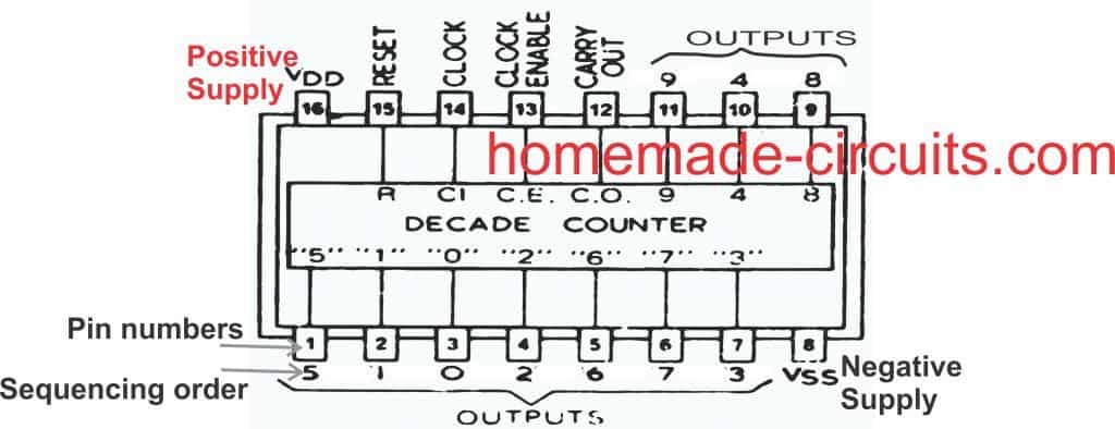
Let’s understand the pin outs of the IC 4017 in details and from a newcomer’s point of view: Looking at the figure we see that the device is a 16 pin DIL IC, the pin out numbers are indicated in the diagram with their corresponding assignment names.
What do Logic High, Logic Low Mean
The pinout which are marked as outputs are the pins which are rendered logic "high" one after the other in a sequence in response to clock signals at pin#14 of the IC.
"Logic high" simply means attaining a positive supply voltage value, while "logic low" refers to attaining zero voltage value.
When the IC 4017 is initially switched ON, it gets reset, and a logic high appears at pin#3 by default. We will discuss the resetting process in the later paragraphs.
In this position, when the first clock pulse is applied at pin#14, the existing logic high at pin#3 jumps from pin#3 to the next pinout that is pin#2. The logic high remains locked on pin#2 until the next clock is applied on pin#14, which causes the high logic at pin #2 to jump from pin#2 to the next output pinout that is pin#4, and this sequencing of logic high goes on until it reaches the last pinout of the IC which is pin#11, after which the logic high sequence jumps back to pin#3, and the cycle repeats again.
What is the Output pin Sequencing order?
To be precise, the sequencing movement happens through the pinouts: 3, 2, 4, 7, 10, 1, 5, 6, 9, 11...
After pin#11 the IC internally resets and reverts the logic high at pin #3 to repeat the cycle.
Why Pin 15 Should be Grounded
This sequencing and resetting is successfully carried out only as long as pin#15 is grounded or held at a logic low, otherwise the IC can malfunction. If it is held high, then the sequencing will not happen and the logic at pin#3 will stay locked.
Please note that the word “high” means a positive voltage that may be equal to the supply voltage of the IC, so when I say the outputs become high in a sequential manner means the outputs produce a positive voltage which shifts in a sequential manner from one output pin to the next, in a “running” DOT manner.
Pin 14 Needs External Frequency (Clock Signal)
Now the above explained sequencing or shifting of the output logic from one output pin to the next output is able to run only when a clock signal is applied to the clock input of the IC which is pin #14.
Remember, if no clock is applied to this input pin#14, it must be assigned either to a positive supply or a negative supply, but should never be kept hanging or unconnected, as per the standard rules for all CMOS inputs.
The clock input pin #14 only responds to positive clocks or a positive signal (rising edge), and with each consequent positive peak signal, the output of the IC shifts or becomes high in sequence, the sequencing of the outputs are in the order of pinouts #3, 2, 4, 7, 10, 1, 5, 6, 9, 11.
Pin 13 is Opposite of Pin 14
Pin #13 may be considered as the opposite of pin #14 and this pin out will respond to negative peak signals. Meaning if a negative clock is applied to this pin will also produce the shifting of "logic high" across the output pins
However normally this pin out is never used for applying the clock signals, instead pin #14 is taken as the standard clock input.
Therefore pin #13 needs to be assigned a ground potential, that means, must be connected to the ground for enabling the IC to function.
In case pin #13 is connected to positive, the whole IC will stall and the outputs will stop sequencing and stop responding to any clock signal applied at pin #14.
How Pin 15 Works Like reset Pin
Pin #15 of the IC is the reset pin input. The function of this pin is to revert the sequence back to the initial state in response to a positive potential or supply voltage.
Meaning, when a momentary positive voltage hits pin 15, the output logic sequencing comes back to pin #3 and begins the cycle afresh.
If the positive supply is held connected to this pin #15, again stalls the output from sequencing and the output clamps to pin #3 making this pinout high and fixed.
Therefore to make the IC function, pin #15 should always be connected to ground.
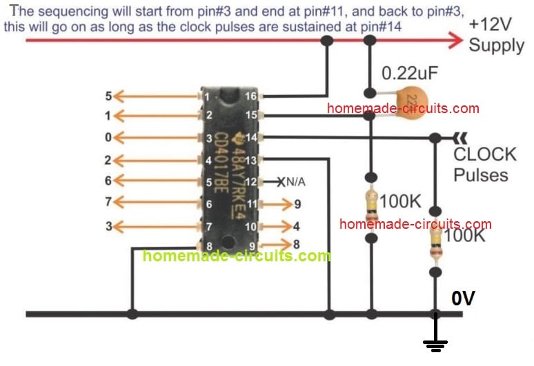
If this pinout is intended to be used as a reset input, then it may be clamped to ground with a series resistor of 100K or any other high value, so that an external positive supply now can be freely introduced to it, whenever the IC is required to be reset.
Using Pin#15 to Reduce the Number of Output Sequence
As I have explained above, there are 10 outputs in the pinout order of 3, 2, 4, 7, 10, 1, 5, 6, 9, 11.
The sequencing begins from pin#3 and ends at pin#11, where the IC resets and the sequence reverts to pin#3 to begin a new cycle.
However, suppose you do not want to use all the 10 output sequences, instead want to limit the sequence to 5 numbers only. Meaning, you want to use the output sequencing in order of 3, 2, 4, 7, 10. The sequence is supposed to begin from pin#3 and end at pin#10 and return back to pin#3.
However, this cannot happen as long as pin#15 is connected to ground. To limit the sequencing to a desired lower count, the pin#15 should be disconnected from the ground line, and connected to output pin which comes just after the last sequence pinout.
In the above example, where we want the sequence to end at pin#10, the next pinout that comes after pin#10 is pin#1, so pin#15 must be connected to this pin#1, to ensure that whenever the sequencing hits pin#1, it is instantly reverted to pin#3 for a new cycle, and the maximum output sequencing is limited to 5 count only.
In the above manner you can limit the output sequencing to any other desired count below 10.
Ground pin and Carryout Pin
Pin #8 is the ground pin and must be connected to the negative of the supply, while pin #16 is the positive and should be terminated to the positive of the voltage supply.
Pin #12 is the carry out, and is irrelevant unless many ICs are connected in series, I will elucidate it some other day. Pin #12 can be left open.
Have specific questions?? please feel free to ask them through your comments...all will be thoroughly addressed by me.
Basic IC 4017 Pinout Connection Diagram
Application LED Chaser Circuit using IC 4017 and IC555
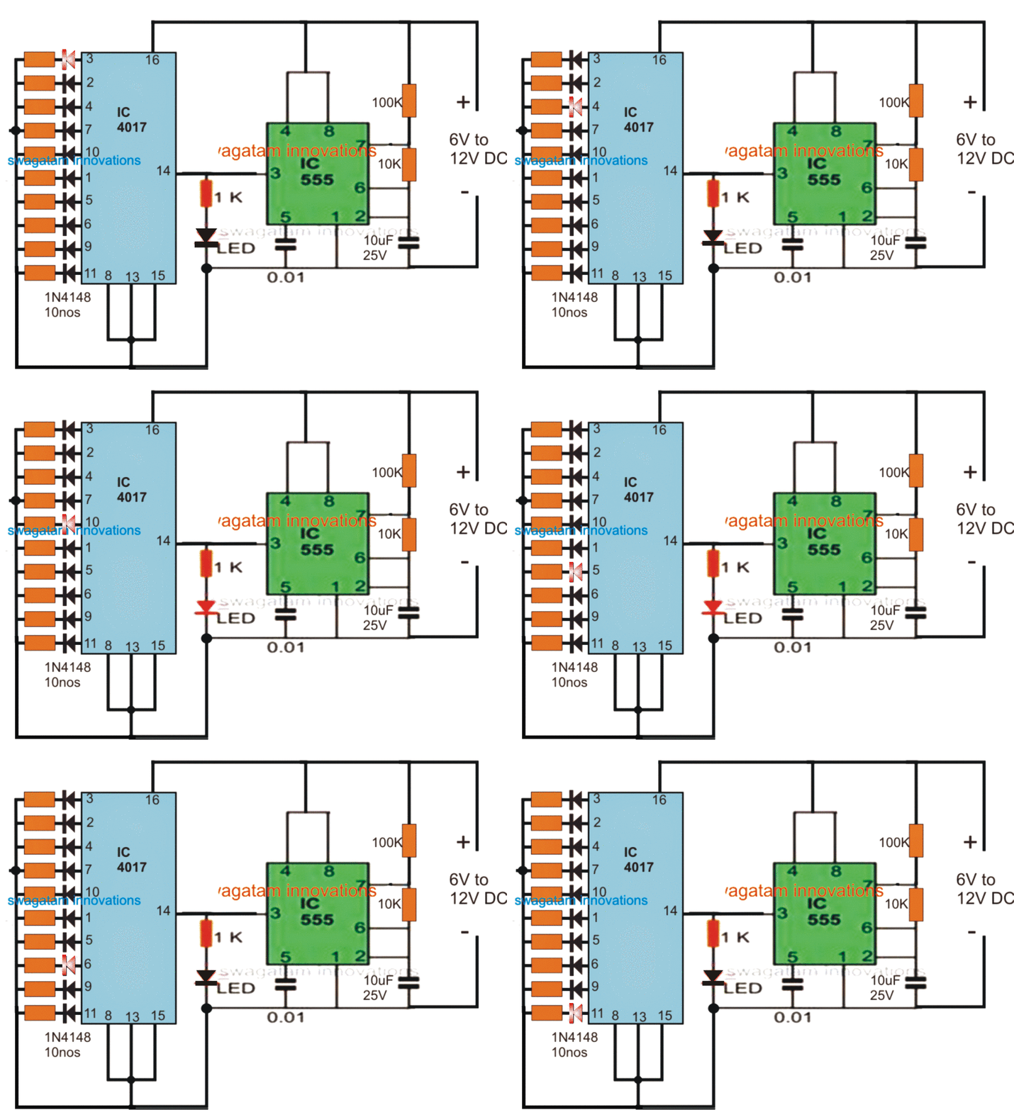
The following example GIF circuit shows how the pinouts of a IC 4017 is usually wired with an oscillator for obtaining the sequential logic high outputs. Here the outputs are connected to LEDs for indicating the sequential shift of the logics in response to each clock pulse generated by the IC 555 oscillator at pin#14 of the IC 4017.
You can see that the logic shift happens in response only to the positive clock or positive edge at pin#14 of the IC 4017. The sequence does not respond to the negative pulses or clocks.
IC 4017 Working Simulation
Video Clip:
How to Cascade Two 4017 ICs for Getting 17 Sequencing Outputs
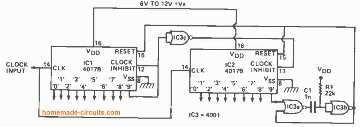
The diagram above shows how to connect two 4017s together to create a 10-to 17 stage counter/decoder. It shows how to cascade two 4017 ICs to get 17 sequencing outputs instead of only 10 from a single IC. The circuit is shown configured to divide by 17.
The clock signal is supplied in parallel to IC1 and IC2. As soon as the count falls below 9, the '9' output of IC1 turns low, causing the clock inhibit pin of IC2 to be set high through IC3c, preventing IC2 from being impacted by the clock signals.
The '9' output of IC1 rises high when the 9th clock pulse comes, inhibiting IC1 from further clocking action, while simultaneously driving the clock inhibit terminal of IC2 low through IC2c, allowing IC2 to respond to further clock signals.
When the 17th clock pulse arrives, the '9' output of IC2 swings high for a brief period, triggering the IC3a -IC3b 15uS monostable. This 15us pulse resets both counters to the empty or '0' states.
After that, the counting sequence starts again by itself. Because the '9' output of IC1 and the '0' and '9' outputs of IC2 are "lost" in the counting process, the circuit only has 17 counter/decoder stages available. By connecting the "free" input pin of IC2a to the matching output pin of IC2, the circuit can be made to count by any number between 10 and 17.
How to Cascade Three IC 4017 for Getting 25 Sequencing Outputs
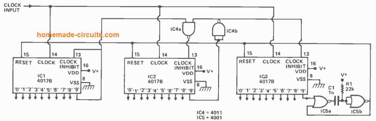
The configuration for creating an 18 to 25 stage counter/decoder from three 4017s can be seen in the diagram above. IC3 is inhibited by IC4b and IC2's low output '9,' whereas IC2 is inhibited by IC4a and IC1's low output '9,' until the 9th clock pulse. Between the 10th and 17th clock pulses, IC1 is inhibited by its high '9' output, while IC3 is inhibited by IC4b and IC2's low output '9'.
Subsequently, between the 18th and 25th clock pulses, IC1 is inhibited by its high '9' output, and IC2 is inhibited through the high '9' outputs of IC1 and IC2 using IC4c, and the whole circuit is reset to the '0' state by means of the IC5a and IC5b monostable.
How to Cascade Four IC 4017 to get 33 Sequencing Outputs
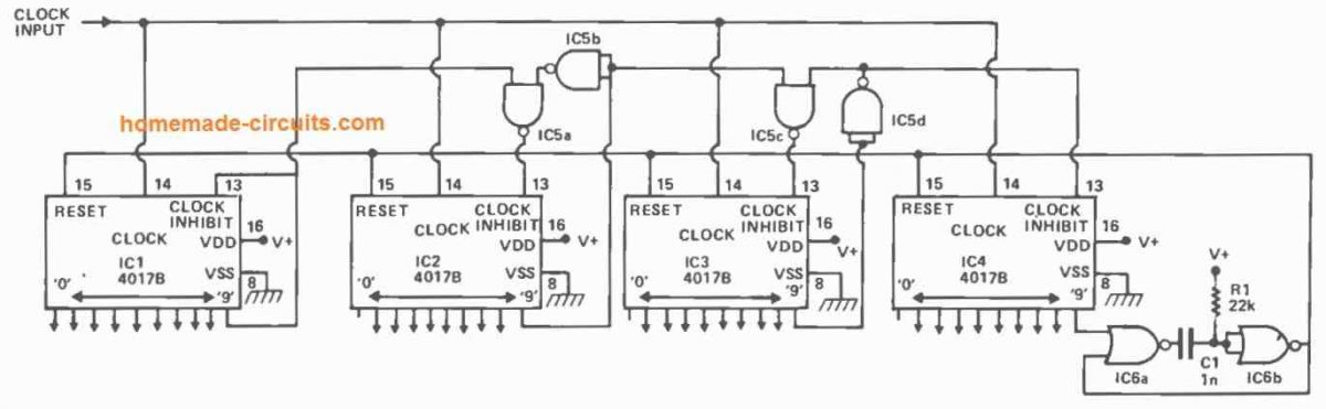
Using a divide-by-33 operation, the above setup shows how to make a 26 to 33 stage counter/decoder set. By interposing extra IC2-1C5a-1C5b stages between 1C2 and 1C3, this design may be extended to provide a ny number of decoded output stages. Each subsequent 40178 stage adds eight decoded outputs to the system.


Questions & Answers
sir,my name is karthie…i need to know where where this was used…?
Hi Karthik, one example can be seen in light chaser circuits, just type "light chaser" in the search box above, you will find the related articles.
Hi I am going to be using this IC in the LED dice with slow down project and I'm looking to connect a sound generator circuit with a flip flop to produce a sound when the LED's come to a stop. I wanted to know what pin on the 4017 will have a positive output once the LED sequence has come to a stop? Hence so I can connect the input of the second circuit (the flip flop) to that pin.
The output will be random and never fixed to a definite pin. It will depend on how many clocks are applied at pin14 of the IC. It will begin from pin3 and sequence by one pinout in response to every positive pulse at its pin14, as soon as it reaches pin11, the sequence returns back to pin3 for repeating the cycle.
Hi I'm making a dice circuit with a cd4017 and a 555timer but I can't get the LEDs that are connected to different outputs on the 4017 to light at the same time. For example, I connected four corners together to make 4, and two middle to make two, but I don't know how to make them both light to make six! It seems like the cd4017 can only have high output on one pin at once? Anything will help, thank you
You can use scrs at the output of the 4017 for latching the switched pinouts of the IC, please refer to the first diagram in this article:
https://www.homemade-circuits.com/2013/03/sequential-bar-graph-turn-light.html
Hi Swagatam
I want to use this IC for 10 random outputs.
According to my understanding, the CD4017 would keep on repeating its output cycle as long as the clock is fed at pin#14. My idea is to use a push-switch, which when pressed momentarily should send clock signals to CD4017. Ten LEDs are so connected that during the counting process no LED should light up. When the clock is disabled and the counting process stops, any one LED should light up randomly.
If the push-switch is used to trigger an monostable oscillator, which in turn activates a clock oscillator, the monostable would always stop the clock at fixed time which ultimately cause the CD4017 to stop it counting process at a fixed output pin.
Please let me have your valued suggestions.
Hi Abu-Hafss,
Yes it is possible, the monostable would also be responsible for feeding the negative to the common ends of the LEDs after it stops the oscillator stage, this would illuminate the particular LED at the end as required by the application
Hi Swagatam
Thanks for such a simple solution. But as I mentioned earlier, the monostable would always stop after a specific time hence, the clock would also stop after that time which ultimately would always light up only one particular LED. How to resolve this issue?
Hi Abu-Hafss,
According to your requirement:
"Ten LEDs are so connected that during the counting process no LED should light up. When the clock is disabled and the counting process stops, any one LED should light up randomly"
That's exactly what will happen if we implement the method suggested by me in the previous comment.
You present question is contradicting the previous question, I did not get it.
By "one particular LED" are you assuming that the 4017 would get reset and pin3 LED would always light up??
No, that wouldn't happen, as soon as the clock stops a random LED could be seen lit up
Hi Swagatam
I mentioned in my very first post, "According to my understanding" which could be wrong. What I assumed is that in an electronic dice circuit, we have to press the ROLL-ON-DICE push button to send the clock signal to CD4017, which will start the counting process until the push-button is released. And during this counting process, the LEDs would turn ON/OFF in the counting sequence until the push switch is released, and then finally one set of LED would light up.
IN SIMPLE WORDS, THE RANDOM SELECTION DEPENDS UPON THE DURATION OF THE TIME FOR WHICH THE PUSH BUTTON IS PRESSED.
Whereas, in my case, if we deploy a monostable oscillator to trigger the clock signal to the CD4017 then the monostable would always stop the clock signal after FIXED TIME PERIOD as set by the timing components. This means the clock signal would always be fed for that fixed time and ultimately the CD4017 would always stop the output at a specific pin.
Hi Abu-Hafss,
OK now I got it, but why do we need a monostable anyway? We can use an astable instead.
…I mean the push button would charge a capacitor, whose level of charge would determine for how long the astable could supply the clocks to the 4017.
Again……., the level of charge of the capacitor will be directly proportional to the time for which the push-switch is pressed.
Monostable oscillator was just my idea as a starting line of action.
I just want a push button to be pressed momentarily which should (somehow) trigger clock signal to the CD4017, always for variable length of time !!!
The capacitor should charge relatively slowly, it should be dimensioned such that it takes about 10 seconds to get fully charged, Since nobody would hold the switch for so long would allow different charge level for the subsequent pressings.
Also the astable whose switch ON time would depend on the charge level of the above capacitor should be dimensioned for producing a very high frequency.
Together, the configuration would force perfect random results from the 4017 outputs, this is what I assume.
may be I misinterpreted your requirement, you don't want the pressing duration to be influencing the result….in that case it will require some thinking and it would make the circuit a bit complex for achieving that.
Hi Swaagatam
Yes, now you got it…..I "don't want the pressing duration to be influencing the result"….:)
Hi Abu-Hafss,
One easy way would be to use another set of 4017/oscillator stage fixed at 1 or 2 Hz sequencing rate, then use these sequencing outputs to provide randomly selected capacitors for the monostable.
This would continue for as long as the system stays powered, that means the monostable would be producing slightly different delays randomly for each flick of its pushbutton.
HMM, AB GURU JEE AAYE RIGHT TRACK PAR 😉
Firstly, for the 1st set (of 4017+oscillator), we have to deploy a non-555 configuration to achieve such low frequency oscillation……right?
Secondly, where the push-button will be deployed?
Lastly, can a Random Bit Generator Circuit be used to achieve the goal instead of your above-suggested configuration?
Thank you Bigboss,
I have seen a circuit of a Random Bit Generator using a few 2N3904 transistors and a TTL NOT gate, but not sure how it would perform for our application.
Another idea is to use an ordinary multicolor LED which generates quite a random automatic blinking rates, this could be integrated to the 4017 pin14 while the monostable output attached with pin13 (after inverting) of 4017 and directly with the common cathodes of the LEDs.
I would be publishing it soon in my blog for you to see.
Hi Swagatam
You didn't replied the first two questions.
Actually, I planned to integrate this circuit in a larger project (LED dance floor) which will illuminate LEDs in different configuration/colors, randomly in response to a foot-tap.
Hi Abu-Hafss,
we can use a 4060 oscillator to facilitate the use of smaller timing capacitor.
The push button could be across pin2 and ground of the monostable.
Can you please explain how you would want to implement the same in your application (LED dance floor)??
Hi Swagatam
Here are the LED dance floor modules (tiles) stacked.
i01.i.aliimg.com/wsphoto/v2/568475299_1/tricolor-rgb-led-dance-floor-sale.jpg
Here they are assembled as floor:

Each tile or module has its complete circuit. Multi-colored LEDs are arranged in various fashion/designs. The circuit can be operated in two modes:
1) AUDIO INPUT: The LEDs will be illuminated in response to the music signals received at the input of the circuit.
2) MANUAL INPUT: Each module is installed with a tap/weight sensor. The circuit will illuminate LEDs in different combination (randomly) in response to a tap or weight change detected by the sensor.
For the 1st option, an audio spectrum circuit can be used. For the 2nd option, I was considering to use the 4017 circuit.
The original circuit is based on microcontroller but, I am trying to do without it.
That's interesting Abu-Hafss, I'll try to include the idea in my blog soon.
Sir how to ensure whether the output pins of 4017 carries the voltage equal to the supply voltage ?
configure the IC as per its standard layout, don't put any clock at its pin14, keep pin14 connected to ground, and measure the output at pin3 or whichever pin may be high at that instant.
…you can also refer to its datasheet for the same…
hello sir how are you now i am a big fan of yours
pls tell me sir how these ic are checked can this be done my multimeter then pls tell me how to check whether ic is faulty or not
Hello Puneet thanks!, there's no easy way of checking ICs such as 4017, the only way is to build a standard configuration and see if all the pins are responding as per the specs.
thank you
me too there is no 4017 in our hometown
this is our project:
T-intersection of 2 way roads.
Requirment of 2 traffic lights.
Red is high for minimum of 5s
Orange/Yellow/Amber is high for 3s fixed
Green is high for minimum of 10s
Also have an indicator that will show where the cars can go (which way)
can you suggest a substitute for 4017?
THANK YOU!! 🙂
will there be other ic that can substitute 4017? we cant find 4017 at our town here is our project
T-intersection of 2 way roads.
Requirement of 2 traffic lights.
Red is high for minimum of 5s
Orange/Yellow/Amber is high for 3s fixed
Green is high for minimum of 10s
Also have an indicator that will show where the cars can go (which way)
THANK YOU!!
you can try IC 4022
WHAT IS THE RESULT IF WE CONNECT 15 TH PIN TO THE 4TH PIN?
How do I get tri color less to run off a cd4017 if ? I need 20ma to leds
I am using a 555 with 4017 to make tri color less with a common cathode dance. How would you do this ?
use the pins 3,4,7 for the LEDs and connect pin7 with pin15
…sorry correction:
use the pins 3, 2, 4 for the LEDs and connect pin#7 with pin#15
hi,i just want to ask,how many voltage power that's in the pin 7(vss),pin 10 and 11(ac power)if my vdd is 12v?if cd4047 just could make the ac signal without amplify so it's not useful than an ac circuit?
Hi Max, the 4017 and N1 are responsible for the chasing action, N2 is used for producing multiple strobe flashes on the LED while it is chasing.
If you are intending to allow the LED to chase upto 7 sequences, in that case you eliminate the N2 output connection with the LED, and connect the LeD cathode ends to ground.
for stopping the chasing after 7 sequences could be done by connecting pin#6 with pin#13…pin#13 being removed from ground
connect pin15 directly with ground
Hj again Swagatam
I really appreciate your patience and extensive knowledge.
I don't think I made myself too clear in my previous post.
What I would like to do is to make 7 outputs strobe very fast for 1 cycle and then all 7 outputs should stay on while a positive voltage is present.
I wish to use 20 leds.
Should pin 15 be grounded via a 100R resistor?
Thanks again and keep up the good work. I learn more every time…
Max
Thanks Max,
In that you can simply connect pin#15 with ground through a 100K or any high values resistor, and also connect a 0.1uF capacitor from pin#15 to positive supply for ensuring that the LEDs always light up from pin#3 whenever the circuit is switch ON
Hello sir
I make this circuit with 10 led.
I want to use this circuit in fence guard for when anyone traped in fence then count 10pulse after than it is off using 555 timer for small time and after than it continuous to work.
But problem is that I give 12v supply using battery.and using second battery I turn on fence guard .but I don't connect fence guard with any connection with counter circuit but every pulse it counts.as I remove 13pin from ground then also counter circuit counts.
As we know fence guard is generate 10kv pulse so due to mutual induction counter circuit start count.
Counter circuit and fence guard machine is totally isolated and keeping distance with 1feet but it counter starts and one by one led glow.
There is no connection between them.
How to remove this effect.
Hello Vikas, I cannot suggest until I see the entire schematic and how you have integrated the two stages with each other.
Anyway, pin#13 must be connected to the positive supply in order to stop the counting, just by removing it from the ground might not correctly inhibit the 4017 from counting….you can do this by connecting pin#13 with pin#11…so that as soon as 10 sequences are over the output locks at pin#11
Hii
I used 4017 to lit 8 rows of led. So I connected output 8 to reset pin . But I doesn't see any sort of output/result. Is it the correct way to connect output 8 directly to reset pin
Hi, the sequence order of the IC is in the following way
#3, 2, 4, 7, 10, 1, 5, 6, 9, 11
Therefore for getting 8 channel effect, you must connect pin#9 with pin#15.
https://www.homemade-circuits.com/2011/12/how-to-understand-ic-4017-pin-outs.html
Pin#8 is the ground pin of the IC…
hii Swagatam
i was trying to build an 8×8 LED display board using 74HC595 shift register to send data to eight anodes. and CD4017 to make sure that only one column is active at time. since 4017 is connected to cathodes of LED matrix, i need active low outputs from 4017 . so i used 2N3904 transistor as driver circuit and as inverter. but i doesnt find any useful outcome. whatever the input at base of transistor the output at collector is grounded ,litting all the leds in the matrix if all anodes are high. …. can you figure out and suggest the changes that should be made in the circuit. im using 5v supply
Hi Ramchandra,
It looks like your IC is faulty or the transistors are faulty,….because all the NPN cannot stay ON together when connected to an oscillating IC 4017 circuit.
You can put LEDs in series with the base of each transistor and check the response..if still you find the base LEDs also ON then definitely that would indicate a faulty IC 4017..make sure you have a 10K resistor at the bases of the transistors
and also make sure the 4017 sequencing is slow enough so that the LED response becomes viewable if it's too fast all LEDs would appear to be glowing together…
Thank you
Hello .
I am tryingto build a Device by using 555 +4017 as an sequencers . Btw I have many questions but the later I'll discuss first I would like to know what ll be the voltage in 4017 outputs. This question is because , I am building a device in which every pins of 4017 outputs have been connected 3-4 LEDs and as well several ICSof 4017 are connected in series with the same outputs configurations so please let me know or if you have any better simple solution for me thankful for your concern ..
Hello,
the output from a 4017 IC will be almost equal to the supply voltage connected to its pin#16…
pls how do i build a a reading lamp of 24 LEDs with 6volt 4.5amp battery ?
make 12 strings of LeDs having 2 LEDs in series on each string…connect all the ends of these 12 strings with the battery terminal with correct polarity.
Good day Sir, I want to 4017 and band switch to on two LED which means I need only two pins to work (0,1) and it should restart again and the pressing of the switch will control it.
How can I do that Sir.
OLuwatoyn, you can try the following concept
https://www.homemade-circuits.com/2013/08/single-push-10-step-selector-switch.html
just replace pin#10 with pin#7…pin#10 can be left unused
Hi thank you for posting this . I built a sequencer for a tone generator and it works but when I turn the rate up to a certain point it stalls and won’t go faster. Recently reconfigured the casing and it suddenly worked in process but now back to stalling any ideas? Thanks
Hi, which IC stalls? is it the IC 4017, can you tell me what exactly happens?? I’ll try to solve it for you….
There is a 555 and a 4017, I’m not sure which one is acting up. What I have is an “Atari punk console” with a four tone sequencer , 4 100k potentiometers for tones and a 500 ohm (I think) for speed. It works but when it is running and I increase the speed, it will only go so fast and then stop on one of the tones. I was adding a keyboard to it the other day and so I was moving the boards around and such and I was testing it while I was working on it to make sure things were still working and I noticed it would then go as fast as I wanted it to, like to infinite. When I repackaged the whole thing and it was finished it was back to stalling again. So im not sure if it’s the 555 or the 4017. Sorry kind of a newbie thanks for quick response.
I figured it out thank you two pins on the 555 needed to be soldered together
OK, good!
yes I was doing a traffic signal using 4017 and 555 timer, and the circuit shows 12 connected to the red LED, I understood the working of yellow and green, but I did not understand why red was connected to pin12
pin#12 of IC 4017 is the carry out pinout, which will enable carrying forward the frequency from the IC 555 to probably a next similar stage.
Hi, thanks for the circuit. Happy Christmas.
I want to build the sequencers for use with eurorack music modules to provide adjustable control voltages. The clock pulse will be supplied whenever a drum pad is played.
Because the clock signal will therefore be intermittent, should I clamp pin 14 to negative supply with a 100K resistor in a similar way to pin 15 clamped to ground?
Hi, Happy Christmas to you too!
yes a 100K to ground is OK, and also a 10uF capacitor in parallel with this 100K will be required, you can tweak this value to suit the needs… this capacitor will actually help to rectify the intermittent signals and enable a constant voltage to the pin14 of the IC….
How do I make a counter count up to five? Pin 10 should be connected to pin 15?
Pin#1 should be connected to pin#15 for getting 5 sequential repetitions.
I was trying to make a calculator out of 3 4017 ICs. But every time that turn it on, all the LEDs start to flash like crazy, so fast that the LED’s are continuously on. The effect is the same as the “4017 AC Detector” that flashes LEDs whenever the 4017 detects AC voltage. (Here is a link to the schematic: ). But you see, I DON”T WANT MY CALCULATOR TO ACT LIKE AN AC DETECTOR! I’ve tried to fix the problem multiple times but nothing would work! Do you have any ideas on how I can fix this problem? Thanks in Advance!
-John Crespo
How did you connect the 3 ICs with each other? Pin#14 will respond to each “high” clock signals and produce a corresponding sequential shift across its outputs. If the clocks are too fast the shifts will be also too fast.
The shown idea is actually not recommended as an AC signal detector, because for any CMOS IC the inputs should never be kept floating, it must be either terminated to a + or a – supply rail, otherwise it may lead to a slow deterioration of the IC performance.
Hello! Thank you for the nice explanation! Here’s my problem: I want to use a 4017 to “downscale” the pulses from a speedometer hall sensor. I changed the gauges on my bike with the ones from a later model, and everything works ok except the speedometer, more precisely its needle goes high, above 120km/h while I barely have 10km/h. The wheels on both bikes have the same teeth number for the hall sensor, so either the sensors are different or the newer gauges have different interpretation of the pulses coming from the sensor. I would try to first divide the pulses by 2 using the 4017, will your circuit work? ? In my understanding I would need to connect the wire coming from the hall sensor to the pin 14 of the 4017 and get the output from one of the output pins, corresponding to what value I want to divide by. Is that correct?
Yes that looks feasible, first the Hall signal will need to be amplified to at least 5V for activating pin#14 of IC 4017. For divide by two output you can use pin#2 as the output and join pin#4, pin#15 together. Make sure pin#14 has a pull down resistor.
How can I measure the signal of the hall sensor? My guess is that the signal should be around 12V, as the bike (it is a maxi scooter in fact) has a 12V electrical installation, I donțt think this signal gets lower voltage anywhere. And what about dividing by 3 or 4? Following your explanation, for dividing by 3 I should use pin #3 as output and join pin #5 and pin #15 together, is that right? What value should the pull down resistor on pin #14 should have? And for the rest of the circuit everything should be left as in your schematics right? I mean I still have to also connect pin #14 to GND using a 100K resistor and also to connect the pin #15 to positive supply using a 0.22uF capacitor and to GND using a 100k resistor.Really sorry for so many questions, I am below newbie level in circuitry, but at the same time would be easier for me to just get the right sensor and cable from the second bike, but I just want to have some fun building this divider, maybe, just maybe it will work. I have everything ready in front of me to build the thing. Thank you for your time, patiently waiting for reply, cheers.
Check to what supply voltage the Hall effect’s supply pin is connected, if it’s 12V then the output will be also 12V, and thn you can connect it directly with the pin#14 of 4017.
Don’t use the pin#3 as the output, instead use the last pin in the order. The order of sequence will be: 3, 2, 4, 7, 10, 1, 5, 6, 9, 11.
If you want to divide by 3, then you will have to use pin#3,2,4 an connect pin#15 with the pin that is next to the last pin in the order, here it will be pin#7 because it is next to the last pin pin#4.
But as shown in the basic diagram, the pin#15 is connected with a 100K to ground. In your case disconnect the end of this resistor from the ground and connect it with the pin#7. Let the 0.22uF be as is.
In the basic diagram a 100k pull down is already shown at pin#14…so you can keep it exactly as shown, no need of adding any extra resistor.
One more time, just to make sure I got this right:
To divide by 2:
– use pin #2 as output
– join pin #4 with #pin15 with a 100k resistor in between.
– no resistor between pin #15 and GND.
To divide by 3:
– use pin #4 as output
– join pin #7 and pin #15 with a 100k resistor between them
– no resistor between pin #15 and GND.
Is this right or I am 100% dumb?
That’s perfectly correct!
Hello again. I am a bit deluded… my circuit doesn’t seem to have any effect on the hall signal. I have tried dividing by 2 and by 4, but the needle still goes to full. To divide by 4 I have connected pin #7 to output and joined pin #10 with pin#15 via 100k resistor. I suppose that is correct. Now, what if I would like to divide straight by 10? I presume that I have to use pin #11 for output, but what pin needs to be tied to pin #15 in this case? Thanks
Hello, if its not working with divide by 2/4 then it might not with divide by 10 either because the problem may be somewhere else!
Connect LEDs from the 2 or 4 pins to ground via 1 K resistors for each LED, and check the response. The LEDs must sequence verifying the hall signal processing correctly.
For divide by 10 connect the pin#15 as shown in the basic diagram, that is to ground via 100K resistor.
Hi sir.
Is it possible to control 2 switches(a momentary switch and a latching switch) using a single push button to switch both switches initially then momentary switches off when button is released and when the button is pressed again, it switches off the latching switch without interfering with the momentary one?
Hi aBhunu,
Do you mean to control two relays, one momentary and another latching?
Yes, that’s exactly my inquiry and whether if its possible to use the same push button to switch off the latching one.
You can try this:
Please remove the capacitor at pin2, replace it with a wire link
Waal, thanks very much let me try it. You are the best.
Glad to help!
Hello Swagatam,
I have an issue which I don’t understand. Perhaps you can help.
I have the following IC’s – a 555 timer, 4081 ‘and’ gate and then 2 x 4017’s
The first 4017 must complete it’s cycle before the second 4017 starts it’s cycle.
pin 3 of the 555 provides output to pin 2 of the 4081 and pin 14 of the first 4017, Pin 3 of the first 4017 resets the second 4017 thru pin 15 (of the second 4017)
Pin 9 of the second 4017 resets the first 4017 thru pin 15.
The problem that I am having is that pins 1 and 3 of the first 4017 output both hi and lo signals. All other outputs on either 4017 are fine.
I will probably have to send you a diagram. Can you please provide me with a link address or email to do this.
Hello Royden,
Can you please upload the pic to any “free image hosting site” online and provide me the link here, I’ll check it and try to solve it for you!
Hi Swagatam. Do you need to password to see the image?
Password is not required, there are many free image hosting sites which can be used for uploading images and for sharing them through the given links
I have put 100K resistors connect to ground on both 4017’s on pins 14 and 15 as you explanation above suggests. Connecting pin 13 on the first 4017 doesn’t work.
Hi Royden, the link that you gave me is not opening, shows an error 404 not found.
https://photos.google.com/photo/AF1QipMyKtf26XKQqhfpS4p0JTTCtxo90joDW0kBOBdR
I’m trying to build a circuit from a book. The first game uses the 4017 and 555 ICs and has a switch between pins 5 and 15 to allow switching between cycling through 6 LEDs or 10 LEDs, with a 56k resistor betwen pin 15 and +9v when the switch is open. I can get it to cycle through 6 LEDs but when switching to 10 it just freezes on LED 1.
I’ve tried varying various component values without success but I’m out of ideas. Any thoughts?
Dear sir. i want to make only 3 LED running light continuously to one side, (not chasing). how i can do that please explain? and also i want to get above running 3 led’s Positive side to be common, is that possible sir?
Jayanth, running effect and chasing effect are one and the same, for 3 LED chasing effect disconnect the 100k of pin15 from ground and connect it with pin7
Hello sir recently i have encounter the problem. I connect one single 555 output to two 4017 ic with a relay as shown in diagram. I want to connect it to my CAR backlight. whenever the car brake applied the backlight led will be dual strobe and when the car head light is on the Backlight will be act as Knight Rider LED sequence. My problem is when I connect the circuit the 1st dual flash light not blink. It is blink only below 7-8volt.
Hi Chandra, you can add a 7809 IC for regulating the voltage to the IC 555/4017 circuit, this might ensure that your circuit runs correctly even at 12 V and higher. Also make sure to add a 100uF/25V capacitor right across the supply terminals of the IC 4017 to suppress electrical spikes.
Hi Swagatam, I hope you are doing well in these troubling times. May I ask if this circuit could be expanded to a total of 60 leds. The reason I ask is I am wanting to have 60 leds to represent the seconds of a clock, so one would come on then go out then the next one and so forth and keep revolving.
Regards Geoff
Hi Geoff, you can cascade any number of 4017 ICs by connecting them in the following manner:
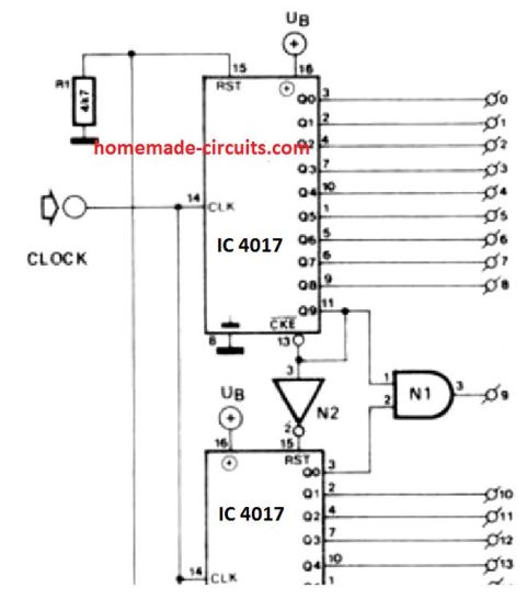
N2 can be any NOT gate such as from the IC 4049, and N1 can be any NAND Gate such as from IC 4011
Hi sir.
How can I force output to low when 555 timer in astable mode is low in repeating manner?
For example when input clock is high for 1 s then after 1 s and before second clock high, output remains low? Not simultaneously?
Thank much
Hi Samo, which output are you referring to, is it 4017 IC output, that may not be possible, because the output of 4017 will get latched to high with each input pulse
Hi Swagtam, i recently made the led chaser circuit using 555 and 4017 like a turn indicator like AUDI CAR in which output 1 to output 10 will high one by one but no low from beginning. But after output 10 all led will LOW mad high one by one. I have connected 4148 diode from output2 to output1. Output3 to output2 and so on. But the circuit show no such effect. It only show on-off from output1 to 10 one by one..pls guide