In this article, I will try to explain how to connect the input and output pinouts of the bilateral switch IC 4066. We will learn how to correctly configure and use the IC 4066 pinouts in a circuit.
The 4066 actually performs the role of an analogue switch. The 4066 is an integrated circuit made up of switches intended to switch analogue signals through digital control.
This implies that when an analogue signal is applied to the switch's input, it will only ever reach the switch's output if a HIGH digital signal is sent to the control (or enable) input.
We can therefore send an analogue signal from the input terminal to the output terminal of the switch by feeding a HIGH digital signal into the control terminal.
A bilateral switch gets its name from the fact that it can work in both directions. This implies that the input can be applied on either side of the switch. Consequently, depending on which side is the input, current might flow in one way or the other.
Main Features of IC 4066
- Basically, a 4066 IC based bilateral switch functions like a single pole, single throw switch.
- The 4066 device consists of 4 built-in switches and thus it is a quad bilateral switch IC.
- There is just one input and one output terminal per switch.
- Additionally, every switch has a control or enable terminal. The control or enable terminal must be HIGH in order for signals to flow from the input terminal to the output terminal.
- To make the control terminal HIGH we must have to supply +5V to it.
- The +5V at the control terminal enables the associated switch to be closed, so that the input signal is able to pass through to the output.
- There won't be any output if the control or enable switch is not connected to +5V or kept deactivated. When the control switch is set to HIGH, the switch closes and an output becomes possible.
- Therefore, the switch is open or turned off when a LOW or a ground is applied on the control terminal. The switch is closed or ON when a HIGH signal is applied on the control terminal.
- The 4066 IC could be operated using a supply voltage range between 5 V and 15 V.
- Maximum output current or the load current must not exceed 10 mA.
The following circuit demonstrates the fundamental operation of the 4066 chip. In this operation we will see how external analogue signals can be controlled through two of its switches, by applying digital signals to the ICs relevant control terminals.
Components Needed
- 4066 Quad Bilateral Switch Chip - 1 no
- Pushbutton Switches - 2 nos
- 10KΩ resistors - 2 nos
- Multimeter to check signal output
The 4066 IC is a quad bilateral switch chip since it consists of 4 in-built switches.
The IC has a total of 14 pinouts.
The complete pinout details of the IC 4066 can be learned from the following diagram:
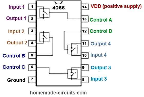
As we know, the IC 4066 is a quad bilateral switch IC, which means it includes 4 switches. The internal switches can be visualized in the above IC pinout image. Each switch is made up of an individual input, output and a control pinout.
The VDD pin 14 indicates the positive supply pin of the IC, and the ground pin 8 is the negative supply pin of the IC.
How to Connect and Use IC 4066 Circuit
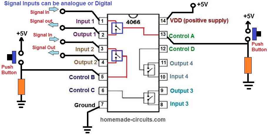
- Referring to the above 4066 connection diagram, we connect +5V supply to VDD, pin 14, and ground 0V supply to pin 7. In doing so, the chip is given adequate power.
- Only two of the four switches are used in this example circuit.
- We supply an analogue signal to the inputs pin#1 and pin#3 of the two switches. This analogue signal can be a simple sine wave or an audio frequency, or a digital signal.
- A pull-down resistor along with a push-button is connected to the control pin#5 and pin#13 of the two switches.
- As long as the push-button is not pressed, the signal is LOW by default on the control pins.
- When the push-button is pressed, the signal becomes HIGH on the control pins.
- When the control pins become high, input signal is allowed to pass into the output pins.
Circuit Description
Therefore, the push-button for each of the switches has to be pressed in order for this circuit to function. This makes it possible for the input analogue signal to reach the output.
If the push-buttons are not pushed, no signal is sent to the outputs.
It simply means that, the analogue signal (or digital signal) at the input will appear at the output only when you press the push-button.
On the other hand, if the push-button is not pressed, the input signal is never allowed to reach the output.

Questions & Answers
Hi, How to make a switch like ON-OFF-ON by using only MOSFETs or transistors can you please suggest me?
Hi, you can do it by doing the following connections:
Take any N channel mosfet
connect the load between its drain and the positive line.
Connect a 1K resistor between its gate and the positive line.
Connect its source with the negative supply line.
Connect a push button switch between its gate and the negative supply line.
can you help me about analog switching for discharge of capacitor
can you please give me more details…
Good night my friend Swagatam!
I planned to make a simple light switch using a PIR. I used 4 LEDs as a light source. When connected to a 12v power supply in series, all LEDs light up as they should.
I decided to make an LED switch based on CD4066, use it as a regular + 12v power switch. I connect the control output of the PIR to pin 13, we have 3.3v at the output. I use lpins 2 and 3 as a normal switch on the + 12v power bus. Everything is working.
BUT! In the absence of movement at the output of the motion sensor 0v, however, the LEDs glow a little and glare. When a signal appears on the motion sensors, all diodes light up perfectly in normal mode.
I just can not cope with the glare of the LEDs in the absence of control voltage. I tried to replace the key switch with a mosfet. The effect is the same, LED glare appears. Somehow there is a power supply through the CD4066 pins even without a control signal on it.
I tried to put a 1N4007 diode as is usually done for a relay. Doesn’t help at all. Basically, I don’t want to put a relay as a switch, so I’m experimenting with this IC.
Perhaps you can help me solve this problem?
Studying the microcircuit, I realized that the CD4066 switches are also based on the mosfet. Maybe the mosfet is not at all suitable for simply connecting an actuator to power?
Is there a way to remove LED glare in this wiring diagram?
Respectfully,
Jorge
Hello Friend Jorge,
For the control pin#13 of IC 4066, the switch connections are pin#1 and pin#2, I hope you have used pin#1 and 2 as the switch for the control input pin#13.
The small illumination on the LEDs could be due to some leakage voltage from the IC 4066.
Did you check the voltage across the LEDs when the PIR is switched OFF and output is 0V?
The LED might show a dim illumination even if there’s 1V present across the LEDs.
Please check the voltage across the LEDs to ensure there’s only 0V across them.
Also try adding a 1K series resistor for the pin#13 control input or try 10K. If possible try 3.3 V for the pin#13 control voltage and check the response.
Bonjour
Je suis Français , je désirerai une traduction en français , est ce possible
Cordialement
JP
Hello, you can right click on the screen and select the Google translation option and get it translated to French.
Goodnight
Could make a tutorial explaining along the lines of the explanation with examples of 4066, explain about 4051,4052,4053
Thanks in advance for your attention
Abr
Thank you Carlos! Yes, please send the tutorials! If they are not published anywhere else then I will post it in this website!
Goodnight
There was an error in the translator, I’m asking for a tutorial on integrated circuits 4051,4052,4053
Grateful for the attention
OK, noted, if possible I will try to post them soon. Thanks for the feedback