An Arduino three phase inverter is a circuit which produces a 3 phase AC output through a programmed Arduino based oscillator.
In this post I have explained how to make a simple microprocessor Arduino based 3 phase inverter circuit which could be upgraded as per user preference for operating a given 3 phase load.
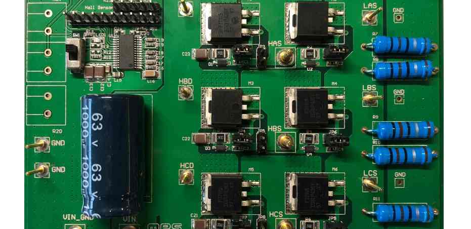
We have already studied an effective yet simple 3 phase inverter circuit in one of our earlier posts which relied on opamps for generating the 3 phase square wave signals, while the 3 phase push pull signals for driving the mosfets was implemented using specialized 3 phase driver ICs.
In the present concept also we configure the main power stage using these specialized driver ICs, but the 3 phase signal generator is created using an Arduino.
This is because creating an Arduino based 3 phase driver can be extremely complex and is not recommended. Moreover, it is much easier to get off-the-shelf efficient digital ICs for the purpose at much cheaper rates.
Before building the complete inverter circuit, we first need to program the following Arduino code inside an Arduino UNO board, and then proceed with the rest of the details.
Arduino 3 Phase Signal Generator Code
// Arduino 3 phase generator code by Swagatam (homemade-circuits.com)

void setup() {
  pinMode(13, OUTPUT); // Phase A
  pinMode(12, OUTPUT); // Phase B
  pinMode(8, OUTPUT);  // Phase C
}

void loop() {
  // Each phase gets 120 degree shift
  // For 50Hz: 1 cycle = 20ms, so 120° shift = 6.66ms
  // Half wave per phase = 10ms, HIGH for 6.66ms, then next

  // Phase A HIGH
  digitalWrite(13, HIGH);
  digitalWrite(12, LOW);
  digitalWrite(8, LOW);
  delayMicroseconds(6666);

  // Phase B HIGH
  digitalWrite(13, LOW);
  digitalWrite(12, HIGH);
  digitalWrite(8, LOW);
  delayMicroseconds(6666);

  // Phase C HIGH
  digitalWrite(13, LOW);
  digitalWrite(12, LOW);
  digitalWrite(8, HIGH);
  delayMicroseconds(6666);
}
The assumed waveform using the above code could be visualized in the following diagram:
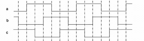
Once you have burned and confirmed the above code in your Arduino, it's time to move ahead and configure the remaining circuit stages.
For this you will need the following parts which hopefully you might have already procured:
Parts Needed
IC IR2112 - 3 nos (or any similar 3 phase driver IC)
BC547 transistors - 3 nos
capacitor 10uF/25V and 1uF/25V = 3 nos each
100uF/25V = 1no
1N4148 = 3nos (1N4148 is recommended over 1N4007)
Resistors, all 1/4 watt 5%
100 ohms = 6nos
1K = 6nos
Constructional Details
To begin with, we join the 3 ICs to form the intended 3 phase mosfet driver stage, as given below:
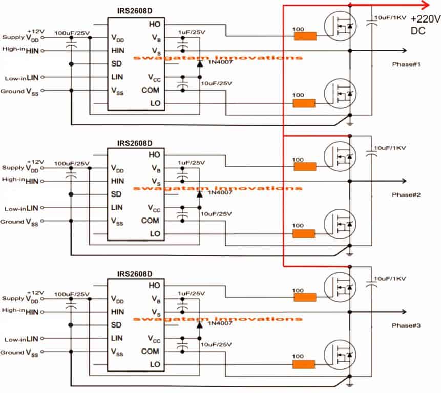
Once the driver board is assembled, the BC547 transistors are hooked up with the HIN and LIN inputs of the IC, and illustrated in the following figure:
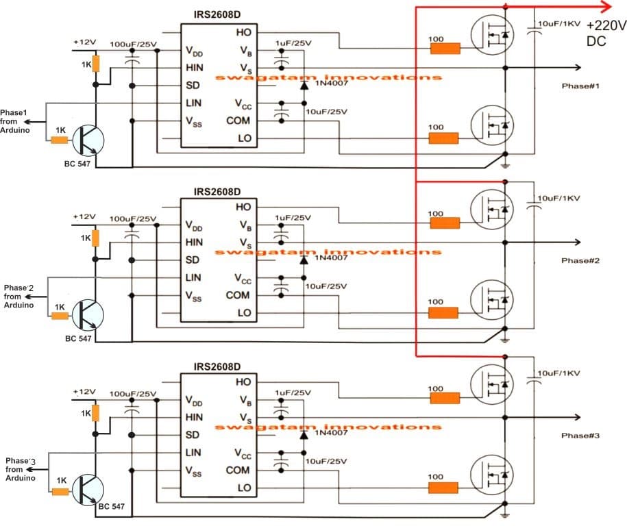
Once the above designs are constructed, the intended result could be quickly verified by switching ON the system.
Remember, the Arduino needs sometime to boot, therefore it is recommended to switch ON the Arduino first and then switch ON the +12V supply to the driver circuit after a few seconds.
How to Calculate the Bootstrap Capacitors
As we can see in the above figures, a circuit requires a couple of external components near the mosfets in the form of diodes and capacitors. These parts play a crucial role in implementing precise switching of the high side mosfets, and the stages are called bootstrapping network.
Although already given in the diagram, the values of these capacitors could be specifically calculated using the following formula:
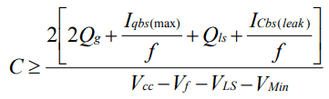
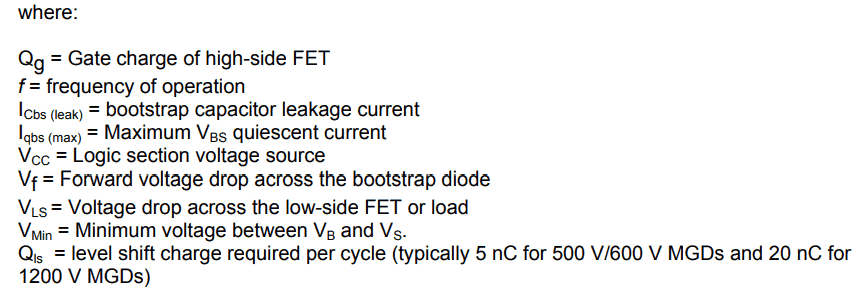
For getting quick results, you can use this Bootstrapping Calculator
How to Calculate the Bootstrap Diodes
The above equations can be used for calculating the capacitor value for the bootstrap network, for the associated diode we have to consider the following criteria:
The diodes activate or are enabled in the forward bias mode when the high side mosfets are turned on and the potential around them is almost equal to the BUS voltage across the full bridge mosfet voltage lines, therefore the bootstrap diode must be rated enough to be able to block the full applied voltage as specified in the specific diagrams.
This looks fairly easy to understand, however for calculating the current rating, we may have to do some math by multiplying the gate charge magnitude with the switching frequency.
For example if the mosfet IRF450 is used with a switching frequency of 100kHz, the current rating for the diode would be around 12mA. Since this value looks quite minimal and most diodes would have a much higher current rating than this normally, specific attention may not be essential.
Having said that, the over temperature leakage characteristic of the diode can be a crucial to be considered, especially in situations where the bootstrap capacitor may be supposed to store its charge for reasonably sustained amount of time. In such circumstance the diode will need to be a ultra fast recovery type to minimize the magnitude of charge from being forced back from the bootstrap capacitor towards the supply rails of the IC.
Some Safety Tips
As we all know that mosfets in 3 phase inverter circuits can be quite vulnerable to damage due to many risky parameters involved with such concepts, especially when inductive loads are used. I have already discussed this elaborately in one of my earlier articles, and it is strictly advised to refer to this article and implement the mosfets as per the given guidelines.
Using IC IRS2330
The following diagrams are designed to work as a 3 phase PWM controlled inverter from an Arduino.
The first diagram is wired using six NOT gates from the IC 4049. This stage is used for bifurcating the Arduino PWM pulses into complementary high/low logic pairs so that the a bridge 3 phase inverter driver IC IC IRS2330 can be made compatible with the fed PWMs.
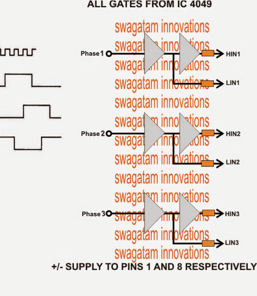
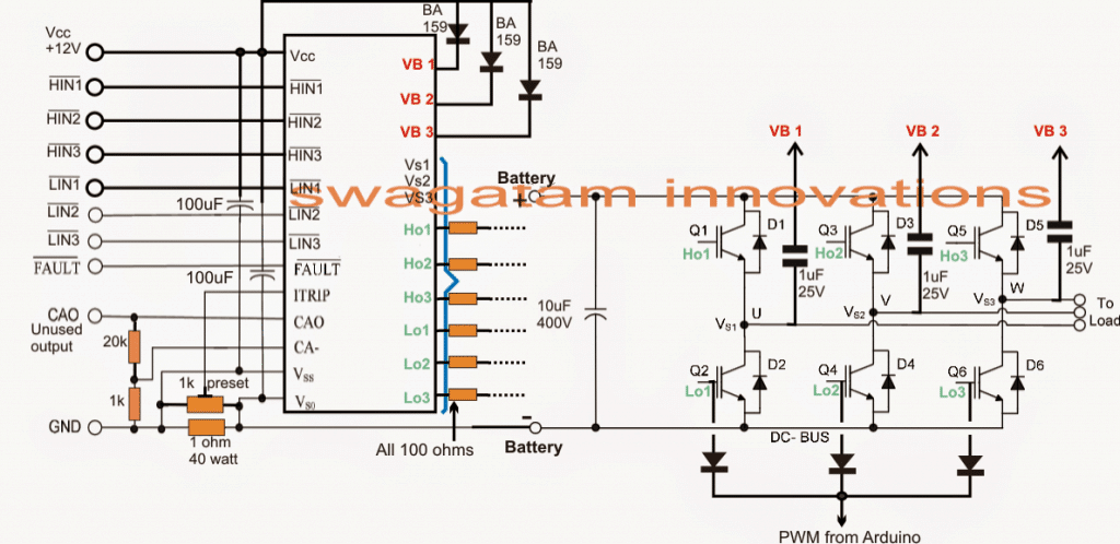
The second diagram from above forms the bridge driver stage for the proposed Arduino PWM, 3 phase inverter design, using the IC IRS2330 bridge driver chip.
The inputs of the IC indicated as HIN and LIN accept the dimensioned Arduino PWMs from the NOT gates and drives the output bridge network formed by 6 IGBTs which in turn drive the connected load across their three outputs.
The 1K preset is used for controlling the over current limit of the inverter by suitably adjusting it across the shut down pin of the I, the 1 ohm sensing resistor may be reduced appropriately if the current a relatively higher current is specified for the inverter.
Wrapping Up:
This concludes our discussion on how to build an Arduino based 3 phase inverter circuit. If you have any further doubts or questions on this subject please feel free to comment and get the replies quickly.
For the PCB Gerber Files and other related files you can refer to the following link:
https://drive.google.com/file/d/1oAVsjNTPz6bOFaPOwu3OZPBIfDx1S3e6/view?usp=sharing
The above details were contributed by "cybrax"


Questions & Answers
Good day sir.. Please sir I need your assistance I want to produce a pure sinewave solar inverter that can carry 5 air conditioner of 5horse power for up to 8 to 12 hrs…. Please Sir I need the diagram and the quantities of solar panels with the watts and the batteries with the current ratings….. Thanks sir and God bless you
Thanks Emmie, Please see this article, you will get all the details regarding the required calculations:
https://www.homemade-circuits.com/2013/05/how-to-calculate-and-match-solar-panel.html
Let me know if you have further queries!
sir can u tell that is the pin VSS and pin COM..from ic ir2110 are corrected direct to the input ground of igbt?…I’m confused because my igbts r getting hot even on 12vdc input…
hi sir can u plz explain if the VSS pin and COM.pin of ic ir2110 are connected to the ground of input dc voltage…I’m confused because my igbts r getting hot even on 12 CDC
Hi Ahmed, yes all the common grounds must be joined together according to the datasheet, otherwise the devices will not conduct.
You can disconnect the grounds and check whether your IGBTs work or not.
hi, please can i write this code to Atmega328p
sorry, I am not sure about it!
Hello, If you compile and export the compiled hex file from your arduino IDE to your local system folder, the you can burn the hex file into Atmega328P microcontroller IC using Universal USB programmer. I have tried that with arduino sketches.
another way to do that is to upload the sketch into Atmega328P using arduino UNO board after that, remove the IC from the arduino board and then build the circuit on your own PCB or veroboard using 14×14 (28pins) IC socket after which you can now socket your programmed Atmega328P IC into the IC socket.
NB: IF YOU ARE USING A BRAND NEW ATMEGA328P APART FROM THE ONE THAT COMES WITH THE ARDUINO UNO BOARD, THEN YOU MUST SET THE FUSE BIT, LOCK BIT etc AND UPLOAD BOOTLOADER TO THE IC BEFORE IT CAN ACCEPT THE UPLOADING OF SKETCH THROUGH ARDUINO BOARD. OTHERWISE, GO FOR THE FIRST SUGGESTION!
Thank You.
hello sir, i need code to vary frequency and voltage of three -phase Inverter to keep v/f ratio constant.
can u help me?
Hi Abhaya, for a 3 phase it looks difficult, it may not be possible from me. Sorry about it!
Hello Dear Swagatam!
Please I want to try this 3 phase arduino inverter but i would like to incorporate a three (3) phase AC voltage meter to display the AC voltages on the 3-phase outputs. Please can you help me with the arduino code too?
Hello Kingsley, I am sorry, coding can be difficult for me because I haven’t mastered Arduino yet
OK boss.
Thank you.
hi dear,
i want to use pwm signal from micro-controller unit.but i dont know how to control frequency. pls tell me if i use PWM controller as your previous circuit to the bridge mosfet on the low side.. is it possible for controlling?
another problem is that ,i made a DC bus using 680uf 400v capacitor .But when i connect with mosfet terminal. it created sparks and mosfet has been damaged. Actually how many value of capacitor will be needed for pure DC filtering.?
thanks
Hello, where do you want you use PWM? Please provide link of the article, so that I can understand correctly.
Hi dear i want to make a 3 phase convetr for 20hp moter ,,,i have 30 soler panal 340w 30volt please help me
Hi, you can implement the design explained in the above article, but you may have to use high power MOSFETs for this.
Hello
Can i use this circuit for a 5kW and 50Hz output. Its application is converting DC from solar into three phase AC.
Hello Morgan, yes you can use it for the mentioned application. But please note that the code was referred from a forum, and it’s not verified by me yet.
Hi,
can u please tell me, you connected 1uf/25 b/w Vb &Vs of IR2608D ic and HO Mosfet emitter, when mosfet would be ON then +220VDc would appear here then this above said capacitor would burn due to low voltage rating and reverse polarity?
Hi, I don’t think so the capacitor has to be higher than the MOSFET drain potential. The charge at the MOSFET pushes the existing VDD charge inside the capacitor to a level such that the effective potential applied at the MOSFET gate is higher than the source potential by a magnitude of VDD
i am stuck in to design 3 – phase VFD can you give me any Solution. i try last one month.
please explain your problem, if possible I’ll try to help!
hi, how mush the max ampere i can use in the load
it will depend on the transformer wattage and the battery power specs, it can be any value as desired by you
Hi,
In your diagram you print irs2608d.
However in the listed parts you say IR2112 and I think the pinout in the diagram is for IR2112, because irs2608d has only 8 pins… Please confirm that the irs2608d has nothing to do with this…
Also, you say this:
“if the mosfet IRF450 is used with a switching frequency of 100kHz”. How can you control this frequency?
Regards.
Joao
Hi,
yes you are right, It is IR2112 but you can use IRS2608 also with its own specified configuration. It is easier and will require only one bootstrap capacitor.
The frequency is which is applied on the Hin Lin inputs of the ICs
The IRS2608 uses “complement LIN” instead of LIN. I think I will stick with IR2112 instead…
So, the switching frequency of IRF450 with your arduino code is 50 Hz (very far from 100KHz…)
The resulting 3 phase 220V AC will be square wave? Instead of using a square PWM produced by arduino with the code you’ve posted, could you use a SPWM arduino code instead, (which already has a frequency adjustment with a potentiometer)?
Can this change at the input give you a sin wave at the output with your setup?
That is not SPWM, that is pure sine wave which cannot be used for 3 phase inverter. It will eventually result in square wave at the output and will produce unpredictable effects. You will have to use rectangular wave as described in the above article. External SPWM can be used at the low side mosfets for getting sinewave output
Thank you very much… Then I will stay with your square wave code, but I will improve it to be able to adjust frequency with the potentiometer
“External SPWM can be used at the low side mosfets for getting sinewave output”
Can you provide me a link for that?
You are welcome! No problem!
The 3rd diagram in the following article shows an example how the low side devices of a 3 phase inverter can be controlled using SPM
https://www.homemade-circuits.com/3-phase-induction-motor-speed/
Thanks again,
I’m going to buy STW30N80K5 instead of IRF450 MOSFET. Do you think its a good idea?
The STW is 800V, while IRF is 500V, it is recommended to choose a MOSFET that closely matches the working voltage specs of the system… if you circuit is rated at 310V then you must look for MOSFETs rated within 400V and 500V
Hi,
I’m going to connect 18 solar panels with 35 V each in a serial setup, so I will have 630 V in the DC bus… In the near future, I also want to upgrade to a variable frequency device and I was thinking on using a full rectifier 3 phase bridge with 6 diodes which will give me also close to 600 V DC peak voltage in the DC bus with a small ripple which I think avoids a capacitor…
So, 800 V MOSFET seems good to me…
However I also intend to use this setup right now, to convert 2 phase in 3 phase, feeding L and N in the same 3 phase full rectifier bridge and in that case I will have less then 400 V DV peak in the DC bus and with a bigger ripple. Do you think the same 800 V MOSFET is totally unacceptable?
Another related question… The bigger ripple in the DC bus demands a capacitor? In afirmative case, which one?
All the best.
Regards
Hi, I think it’s fine to use the 800V mosfets, actually it’s the ID that must higher than the required output specs…
For the capacitor you an try 100uF/400V…although higher values will give better results…
It seems too much complicated, but convinced me to use at least the IC IRS2330 approach instead of IR2112. Later maybe I can upgrade to this beauty…
OK, no problem…
I decided to use 1 IRS2330 instead of 3 IR2112 because it’s easier to upgrade in the future to your diagram using the SPWM…
However, you wrote:
“The first diagram is wired using six NOT gates from the IC 4049. This stage is used for bifurcating the Arduino PWM pulses into complementary high/low logic pairs so that the a bridge 3 phase inverter driver IC IC IRS2330 can be made compatible with the fed PWMs.”
Can you explain me better?
In IRS2330, the HIN and LIN are both complementary so I don’t understand the bifurcating diagram where you get HIN through 2 NOT gates and LIN through 1 NOT gate. Is it really necessary to use NOT gates? I think the only thing that would happened if you directly feed the original rectangular wave of the arduino in HIN and LIN would be an out of phase output related to the arduino wave. But would that be a problem?
The IC has 6 inputs ( 3 pairs of HIN/LIN), and the Arduino gives 3 outputs, therefore the Arduino 3 phase signal needs to be divided into six outputs for the 6 HIN LIN inputs of the 3 phase IC, using NOT gates. This can be also done through NPN transistors as shown in the second diagram.
In the second diagram the IC is not the same because the input is not complementary. Just to be sure, can you recheck the bifurcation diagram? It s not making sense to me…
Both the ICs are one and the same with their characteristics, the IRS2330 has the 3 ICs embedded in one that’s the only difference…rest everything is exactly identical, the HIN/LIN are complementary for both the variants.
Please let me know why it is not making sense…the NOT gates are inverters, they will invert the input signal at their output
Because in the datasheet one IC has overscore over HIN an LIN and the other doesnt
Overbar means the specific pins become active when the input signal it LOW. HIN and LIN are always complementary or reciprocal to each other in full bridge ICs as far as I know.
Ok. Then one IC is active when hin is low because it has overbar and the other IC is active when hin is high because it does not have overbar. My point is that the input cannot be the same on both IC
HIN an LIN inputs should never have same polarity at any instant, that’s why we say complementary, meaning equal and uniform but opposing in nature…for example BC547/BC557 transistor, they are NPN/PNP complementary pair.
That’s why I used NOT gates which will invert the corresponding signals, I have already explained this to you in the previous comment
Im not saying that hin and lin could have the same polarity. Im saying that hin_overbar from one IC may have different polarity from hin_WITHOUToverbar of the other IC. Otherwise I cannot undertand why the overbar is there for one IC and not for the other
Lets simplify and forget the 3 phases and think about how to make an inverter from 230 V DC to 230 V AC (not a square wave but a sin wave output)
In reality what I want is something like this:
but WITHOUT the transformer since I already have 230 V DC…
In this site they use a very nice 100 KHz arduino code with 200 points sampling on each 20ms (50 Hz) to build 2 really good complementary SPWM over pins 9 and 10 (not the nasty one I sent you in one of my first posts…) and they say the output in the secondary of the transformer is sin wave. What I don’t understand is why do I have to have the transformer to achieve this and in order to avoid it I have to put lots of extra hardware with more and more SPWM. Please take a look and give me feedback. Best regards.
I have already designed a better one here:
https://www.homemade-circuits.com/arduino-pure-sine-wave-inverter-circuit/
To avoid transformer you will need a H-bridge or full bridge topology for the push pull effect and for AC output, and for this you can try this topology:
https://www.homemade-circuits.com/arduino-full-bridge-h-bridge-sinewave-inverter-circuit/
For implementing this SPWM directly in 3 phase HIN and LIN of a full brdige IC you will need complementary 120 degrees phase shifting SPWM code or circuit. That looks so unnecessarily complex. That is why I designed the low side mosfet control method which is a great and an easy way to achieve pure sine in full bridge transformerless inverter
I know im being a pain to you… Thank you for supporting me. I really need 3 phase and a sin wave output and I dont want 3 transformers. However Im totally lost. The only think I decided was the 800V mosfet that i already buy. Also, since I feel confortable with arduino I want to avoid 555 timers etc and I want to generate spwm, ]pwm, whatever in it. Really (and thinking only 1 phase to simplify) i still dont understand why the rectangular wave works and the spwm does not. After all spwm is rectangular wave with a complex frequency… Please make a simplest as can be complete diagram of your sin wave 3 phase solution using only the arduino as timer because im totally lost at your site.