A very simple yet highly sophisticated modified sine wave inverter circuit is presented in the following post. The use of the PWM IC TL494 not only makes the design extremely economical with its parts count but also highly efficient and accurate.
Audio/Video Representation
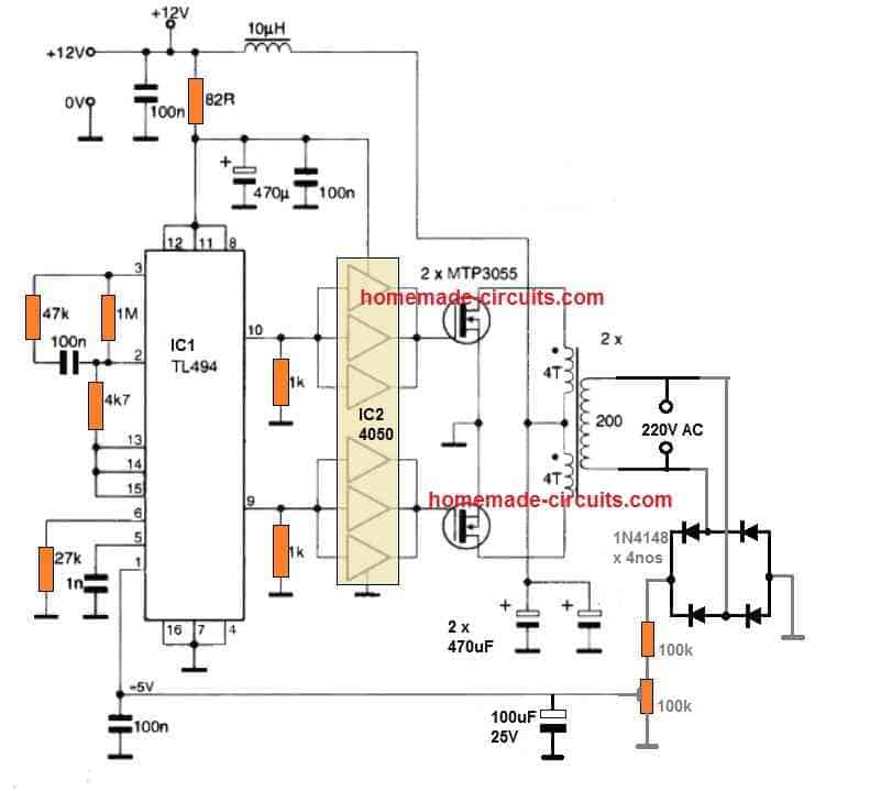
Using TL494 for the Design
The IC TL494 is a specialized PWM IC and is designed ideally to suit all types of circuits which require precise PWM based outputs.
The chip has all the required features in-built for generating accurate PWMs which become customizable as per the users application specs.
Here I have explained a versatile PWM based modified sine wave inverter circuit which incorporates the IC TL494 for the required advanced PWM processing.
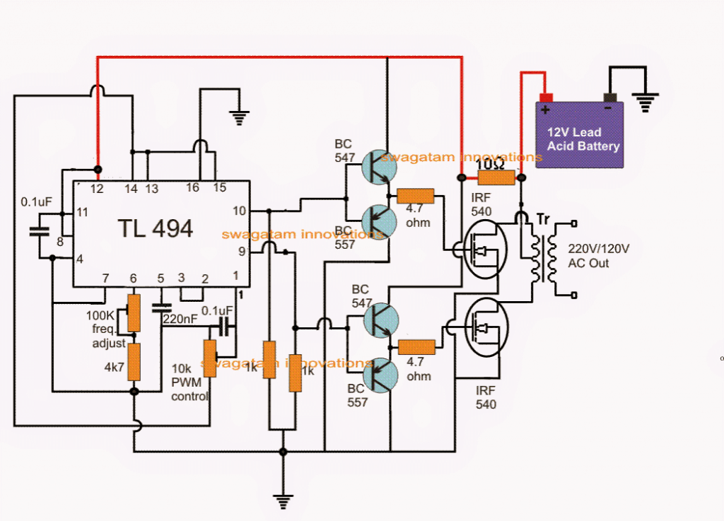
Referring to the figure above, the various pinout functions of the IC for implementing the PWM inverter operations may be understood with the following points:
Pinout Function of the IC TL494
Pin#10 and pin#9 are the two outputs of the IC which are arranged to work in tandem or in a totem pole configuration, meaning both the pinouts will never become positive together rather will oscillate alternately from positive to zero voltage, that is when pin#10 is positive, pin#9 will read zero volts and vice versa.
The IC is enabled to produce the above totem pole output by linking pin#13 with pin#14 which is the reference voltage output pin of the IC set at +5V.
Thus as long as pin#13 is rigged with this +5V reference it allows the IC to produce alternately switching outputs, however if pin#13 is grounded the outputs of the IC is forced to switch in a parallel mode (single ended mode), meaning both the outputs pin10/9 will begin switching together and not alternately.
Pin12 of the IC is the supply pin of the IC which can be seen connected to the battery via a dropping 10 ohm resistors which filters out any possible spike or a switch ON surge for the IC.
Pin#7 is the main ground of the IC while pin#4 and pin#16 are grounded for some specified purposes.
Pin#4 is the DTC or the dead time control pinout of the IC which determines the dead time or the gap between the switch ON periods of the two outputs of the IC.
By default it must be connected to ground so that the IC generates a minimum period for the "dead time", however for achieving higher dead time periods, this pinout can be supplied with an external varying voltage from 0 to 3.3V which allows a linearly controllable dead time from 0 to 100%.
Pin#5 and pin#6 are the frequency pinouts of the IC which must be connected with an external Rt, Ct (resistor, capacitor) network for setting up the required frequency across the output pinouts of the IC.
Either of the two can be altered for adjusting the required frequency, in the proposed PWM modified inverter circuit we employ a variable resistor for enabling the same. It may be adjusted for achieving a 50Hz or 60Hz frequency on pins9/10 of the IC as per the requirements, by the user.
The IC TL 494 features a twin opamp network internally set as error amplifiers, which are positioned to correct and dimension the output switching duty cycles or the PWMs as per the application specs, such that the output produces accurate PWMs and ensures a perfect RMS customization for the output stage.
Error Amplifier Function
The inputs of the error amplifiers are configured across pin15 and pin16 for one of the error amps and pin1 and pin2 for the second error amplifier.
Normally only one error amplifier is used for the featured automatic PWM setting, and the other error amp is kept dormant.
As can be seen in the diagram, the error amp with the inputs at pin15 and pin16 is rendered inactive by grounding the non-inverting pin16 and by connecting the inverting pin15 to +5V with pin14.
So internally the error amp associated with the above pins remain inactive.
However, the error amp having the pin1 and pin2 as the inputs are effectively used here for the PWM correction implementation.
The figure shows that pin1 which is the non-inverting input of the error amp is connected to the 5V reference pin#14, via an adjustable potential divider using a pot.
The inverting input is connected with pin3 (feedback pin) of the IC which is actually the output of the error amps, and enables a feedback loop to form for pin1 of the IC.
The above pin1/2/3 configuration allows the output PWMs to be set accurately by adjusting the pin#1 pot.
This concludes the main pinout implementation n guide for the discussed modified sine wave inverter using the IC TL494.
Output Power Stage of the Inverter
Now for the output power stage we can visualize a couple of mosfets being used, driven by a buffer BJT push pull stage.
The BJT stage ensures ideal switching platform for the mosfets by providing the mosfets with minimum stray inductance issues and quick discharge of the internal capacitance of the fets. The series gate resistors prevent any transients trying to make its way into the fet thus ensuring the operations to be entirely safe and efficient.
The mosfet drains are connected with a power transformer which could be an ordinary iron cored transformer having a primary configuration of 9-0-9V if the inverter battery is rated at 12V, and the secondary could be 220V or 120V as per the user's country specs.
The power of the inverter is basically determined by the transformer wattage and the battery AH capacity, one can alter these parameters as per individual choice.
Using Ferrite Transformer
For making a compact PWM sine wave inverter, the iron core transformer can be replaced with a ferrite core transformer. The winding details for the same may be seen below:
By using super enamelled copper wire:
Primary: Wind 5 x 5 turns center tap, using 4 mm (two 2 mm strands wound in parallel)
Secondary: Wind 200 to 300 turns of 0.5 mm
Core: any suitable EE core which would be capable of accommodating these winding comfortably.
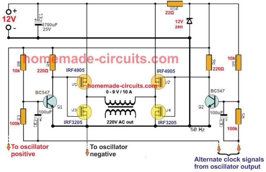
Automatic PWM Voltage Regulation
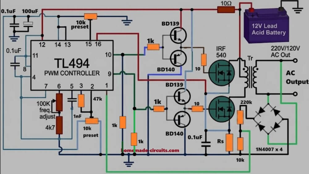
The above diagram shows how the manual PWM control action could be upgraded into a full automatic output PWM control with respect to the output voltage changes.
When heavy load comes on the output side then output voltage may start dropping a bit, so now the feedback voltage at pin 1 also drops together since both are linked.
TL494 reacts almost immediately to that condition and increases the PWM duty cycle automatically.
Because of that, MOSFET stays ON for longer time, transformer transfers more power, and output voltage starts climbing back toward normal again.
In the same way, if output voltage goes too high somehow then feedback voltage also rises, so now TL494 reduces the PWM duty cycle by itself.
That pulls the output voltage back down again near the proper level.
This whole thing keeps happening continuously in the background, therefore output voltage stays regulated automatically even when load conditions keep changing around.
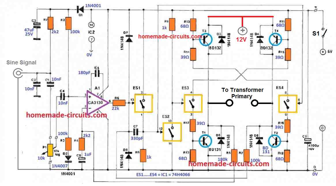
TL494 Full Bridge Inverter Circuit
The following design can be used for making full bridge or H-bridge inverter circuit with IC TL 494.
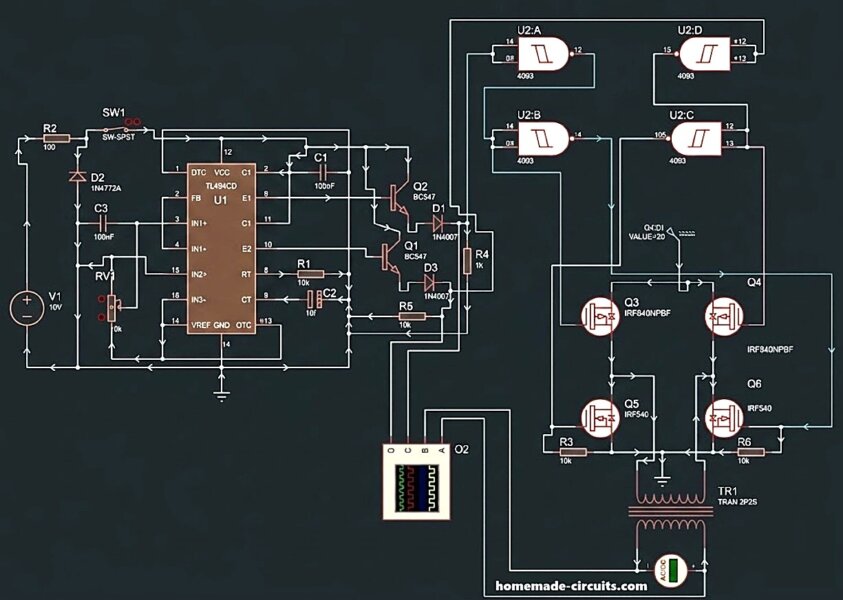
As can be seen, a combination of p channel and n channel mosfets are used for creating the full bridge network, which makes things rather simple and avoids the complex bootstrap capacitor network, which normally become necessary for full bridge inverters having only n channel mosfet.
However incorporating p channel mosfets on the high side and n channel at the low side makes the design prone to shoot-through issue.
To avoid shoot-through a sufficient dead time must be ensured with the IC TL 494, and thus prevent any possibility of this situation.
The IC 4093 gates are use for guaranteeing perfect isolation of the two sides of the full bridge conduction, and correct switching of the transformer primary.
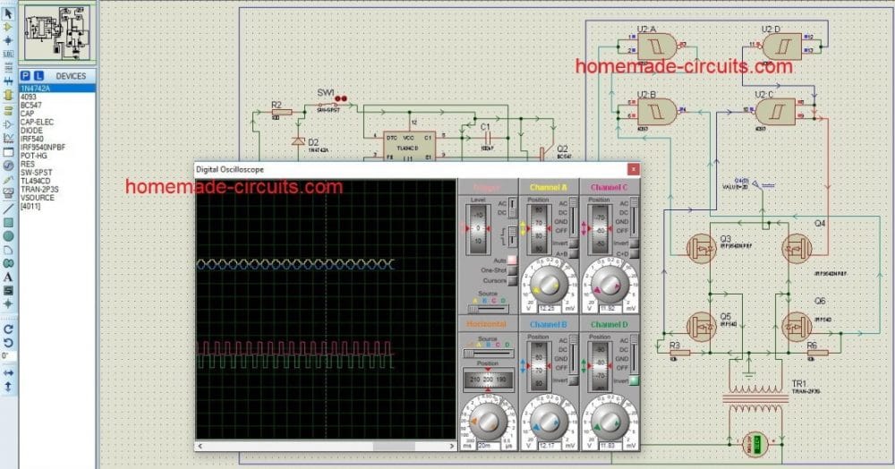
Simulation Results
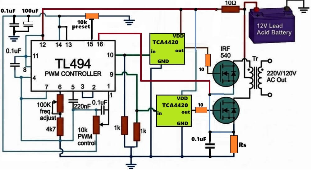
TL494 Inverter with Feedback
A very simple yet accurate and stable inverter circuit using IC TL494 is shown in the below diagram.
The inverter includes a feedback control system for automatic output voltage correction, applied at the error amplifier pin#1 of the IC.
The 100k preset can be adjusted appropriately for setting up the required constant output voltage limit.
The transformer shown is a ferrite core transformer, and therefore the frequency is set at a very high level from the IC. Nevertheless, you can easily use an iron core based transformer and reduce the frequency to 50 Hz or 60 Hz for 120 V output.

Questions & Answers
Hello dear Swagatam. Problem 9x is trying to get TL494 to work with AI. Nothing. Could you please give me a circuit diagram for the following: TL494, frequency 10kHz to approx. 50kHz, shunt 60mV 50A adjustable 10 to 40A with trimmer, with LM311, pin 9 and 10 according to TC4420cpa. Maybe an LED to limit the current. Thank you in advance.
Hey, Mamo, here is the full circuit diagram as per your above request:
From 2016 to date 2025, your page and circuit have changed my life positively, can’t wait to meet you physically my Boss
God bless you
+2349033992354
It’s my pleasure Barnabas. God bless you too!!
Hello swagatam, my question is pin10 and pin9 are the emitters of the internal transistor, why is it been use as switching because that is an emitter follower configuration which is not ideal for switching: I have been confused whether using pin8 and pin11 or pin9 and pin19.
Hi Victor, there’s nothing wrong to use the emitter outputs of the IC E1, E2, for switching the output transistors in an inverter configuration. Alternatively, you can also use the collector ends of the transistor, for switching the output MOOSFETs through pull-up resistors.
Yes, the Emitter terminals may not be ideal if you are configuring them directly with the MOSFET gates without a totem pole driver/buffer stage….and yes, the collector ends can be directly configured with the MOSFET gates without any driver/buffer stages to get a highly efficient switching of the MOSFFETs.
So yes, please use the collector ends C1, C2, pins of the ICs to drive the external MOSFETs, via pull-up resistors of 1k, each between C1 and +positive, C2 and +positive.
from 300 to 500 whatts I don’t want more than that, it’s for lights and for me to be able to work with electronics
Sure, here’s the design you can try:
Just two MOSFETs on each channel will be enough, 5 are not required…
best regards from Cuba brother, I would like to know how to make it a modified wave to an iron transformer. Here the current is very unstable. If you know the news, you will know what I am talking about. This is my WhatsApp +5350482624
Sure brother, I can help you….just tell me how must output power do you need for the load, then I will design it accordingly…
Hi, I have built the circuit but get any output from pin 9 and pin 10. what must be the reason, for 50 Hz what must be the trimpot values. I have changed the trimpots from min to max but no output seen. can some one help , will be welcome. thanks a lot
Hi, please check and confirm that the IC supply pins are getting the DC voltage correctly. Pin#8,11,12 must get the +Ve supply and the pin#16,7,4 must get the ground supply.
Also please check the frequency across the pin#5 capacitor.
The formula for calculating frequency is: f = 1 / RT(ohms) x CT(Farads)
RT is the resistor between pin#6 and ground.
CT is the capacitor between pin#5 and ground.
Please what pin should I modify in a TL494 inverter to make to make the low battery 9V. The inverter turns off at 10.5 V but I have a 3S Li-ion battery which can still go as low as 9V.
Thanks.
TL494 can work with voltages as low as 7V, so 9V should not be a problem, you can use this IC with 9V supply also.
Sir, I have a question, Is it possible to generate bipolar pwm signal by using 555 timer ic?? If yes then how to get that
Hello Anupam,
You will have to connect a BC547 transistor with pin#3 of the IC 555, then pin#3 will generate positive PWMs, and the collector of the BC547 will generate the negative PWM
Yes, I made the circuit in simulation software according to what you said earlier but it is oscillating from 0 to positive high voltage. Maybe I am wrong. So, can you provide the circuit diagram or any other documentation for reference.
The output PWMs at pin#3 of 555 will be zero to positive, that cannot be changed. I did not understand your requirement. Please elaborate what exactly you are looking for?
Dear,
Please I have a question, can use TL494 for boost converter from 12 v to 5 v and the vice versa.
Thank you
YES YOU CAN USE IT
Yes you can.
please can you provide me one circuit for boost up from 5v to 12v
Con el tl494 no puedes aumentar de 5v a 12 v ya que este circuito requiere mínimo 7.5 v de alimentación
You can try the following concept:
https://www.homemade-circuits.com/high-power-dc-to-dc-converter-circuit-12-v-to-30-v-variable/
I have other circuits also without using TL494
Sir, I have been trying to construct the atx using tl494 or sg3525 with ferrite from old TV’s but it used to burn my MOSFET and i.c, it works but with great heat. My RT and CT are 15k and 0.001(102). How can I solve the problem?
Emmanuel, the ferrite transformer is the main component in any smps circuit. If the transformer is not calculated correctly or has even the slightest amount of incorrect winding then the circuit will suffer and the devices will start getting hot.
Hi sir. I’m searching for a diagram of converter that will able to drive a motor pump about 2000VA or more. The out put is 220V. Thank.
Hi Jean, you can probably try the first design from the following article, and upgrade its mosfets and transformer accordingly:
Make This 1KVA (1000 watts) Pure Sine Wave Inverter Circuit
This is an easy and cheap design so the efficiency will be only around 70%
Hi sir. Thanks for quick answer, I’l try it
Sure! no problem…
Thank you for prompt response. Please, Can ferrite transformer high frequency inverter be used to safely power some equipment at home at KHz frequency?
Are there KHz frequency final output inverter in the market?
Can KA7500 or TL494 ic actually generate 50 or 60 Hz frequency(datasheets stated KHz) or how can frequencies of 50 or 60Hz be actually generated from the ic?
Actually the TL494 cannot generate 50 Hz, the minimum is 1 kHz. You can perhaps use a inductive/capacitive filter at the transformer output to clean the high frequency waveform and convert it to normal AC waveform.
You stated that ferrite core transformer can be used. What frequency would the ferrite operate in the inverter. Ferrite core transformer operates at high frequency(KHz) while iron core transformer operates at low frequency(50 or 60Hz) which is the main frequency. The frequency to operate ferrite core transformer is too high for main ac and ac motor etc can not work well at that frequency. Also Can KA7500 or TL494 ic generate 50 or 60Hz wave(datasheets state KHz). Thanks
If ferrite core is used then naturally the frequency cannot be in Hz, it will need to be increased in many kHz
Hi sir, want to build up a inverter using pic as the controller.please,can you give me an article on how to get started on pic controller coding and the ?pin out
Hi Eniola,
you can modify the following circuit as per your specific requirements
https://www.homemade-circuits.com/arduino-pure-sine-wave-inverter-circuit/
Sir,in the first circuit diagram, can I connect the feedback to pin 2 and pin3?since,pin2 is the inverting pin.
John, pin#3 is not the correct pin, you must select one of the error amp inputs. Please see the last diagram.
Okay,I gave pin 1 feedback and pin 2.5v from pin14 using two 5ohm resistors.but, how can I connect pin 3 with pin2? And the resistor value?
Please see the last diagram for all the details.
Or just tell me how pin 1 correct the output.thanks sir looking forward to your quick response
Hi sir, according to your first circuit diagram, you taped voltage from pin 14 to pin 1, what if I fixed it and compare it with pin 2 from the feedback voltage.because, I’m thinking of feeding pin 2 with feedback (non inverting pin) in order to stabilize the output.but, the last circuit diagram shows that pin 1is feed from feedback voltage and pin 2 is a fixed voltage feed from reference voltage (pin 14), but to my knowledge when the output is high obviously the comparator won’t low,it will also be high.but if the feedback voltage is feed to pin 2 it will obviously oppose the output.i I mean when high the comparator Will be low trying to stabilize the output.waiting for your quick response.thanks sir
Eniola, the last diagram with feedback is correct. Pin#2 is an inverting input. The inverting input (-) must be connected to a fixed reference, and the non-inverting (+) must be applied with the feedback signal. The error comparator output must become high to enable output PWM narrowing and output voltage control
Sir, to protect the mosfet from emf voltage.the resistor value for discharge to ground and diode? Thanks sir
The resistor can be 1K across gate/source for 12V….10 ohms for the gate resistor, and 1N4148 parallel to the 10 ohms
Thanks sir,got the message.one more thing sir, can I then connect pin 2 and pin 3 to pin14 ?if yes at what voltage can I I supply them? And finally resistor value for dropping the voltage.thanks sir, looking forward to your quick response.
Eniola, you must do exactly as shown in the diagrams, any other configuration can cause unpredictable results