A flyback configuration is the preferred topology in SMPS application designs mainly because it guarantees complete isolation of the output DC from the input mains AC. Other features include low manufacturing cost, simpler design and uncomplicated implementation. The low current DCM version of flyback converters which include output specification lower than 50 watt are more widely used than the bigger high current counterparts.
Let’s learn the details with a comprehensive explanation through the following paragraphs:
Comprehensive Design Guide for Off-line Fixed Frequency DCM Flyback Converter
Flyback Modes of Operations: DCM and CCM
Below we see the fundamental schematic design of a flyback converter. The main sections in this design are the transformer, the switching power mosfet Q1 on the primary side, the bridge rectifier at the secondary side D1, a filter capacitor for smoothing the output from D1, and a PWM controller stage which may be an IC controlled circuit.
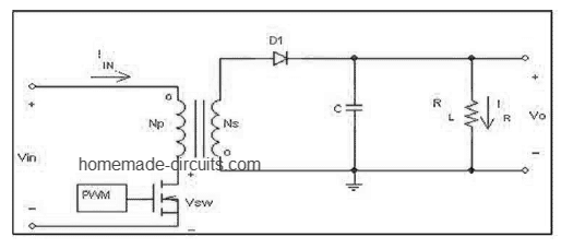
This type of flyback design could have a CCM (continuous conduction mode) or DCM (Discontinuous conduction mode) of operation based on how the power MOSFET T1 is configured.
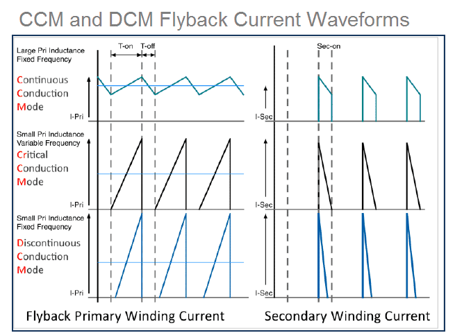
Basically, in DCM mode we have the entire electrical energy stored in the transformer primary transferred across the secondary side each time the MOSFET is turned OFF during its switching cycles (also called the flyback period), leading to the primary side current reaching a zero potential before T1 is able to turn ON again in its next switching cycle.
In the CCM mode, the electrical energy stored in the primary does not get the opportunity to get fully transferred or induced across the secondary.
This is because, each of the subsequent switching pulses from the PWM controller turn ON T1 before the transformer has transferred its full stored energy to the load. This implies that the flyback current (ILPK and ISEC) are never allowed to reach the zero potential during each of the switching cycles.
We can witness the difference between the two modes of operation in the following diagram through the current waveform patterns across the primary and secondary section of the transformer.
Both DCM and CCM modes have their specific advantages, which may be learned from the following table:
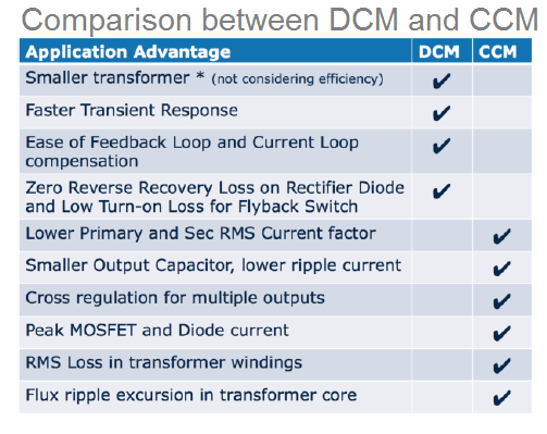
Compared to CCM, the DCM mode circuit demands greater levels of peak current in order to ensure optimal power across the secondary side of the transformer. This in turn demands the primary side to be rated at higher RMS current, meaning the MOSFET needs to be rated at the specified higher range.
In cases where the design is required to be built with limited range of input current and components, then usually a CCM mode fyback is selected, allowing the design to employ relatively smaller filter capacitor, and lower conduction loss on the MOSFET and the transformer).
CCM becomes favorable for conditions where the input voltage is lower, while the current is higher ( over 6 ampere), designs which may be rated to work with over 50 watt power, except for outputs at 5V wherein the wattage spec could be lower than 50 watts.
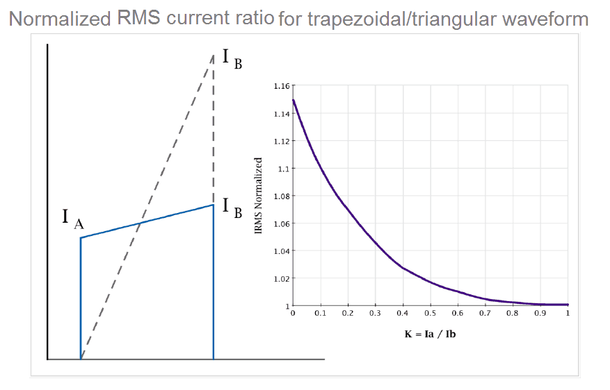
The image above indicates the current response on primary side of the flyback modes and the corresponding relationship between their triangular and trapezoidal waveforms.
IA on the triangular waveform indicates the minimal initialization point which may be seen as zero, at the beginning of the switch ON period of the MOSFET, and also a higher current peak level persistent in the primary winding of the transformer at the time until the MOSFET is switched ON again, during the CCM mode of operation.
IB may be perceived as the finish point of the current magnitude while the mosfet switch is turned ON (Ton interval).
The normalized current value IRMS can be seen as the function of the K factor (IA/IB) over the Y axis.
This may be used as the multiplier whenever resistive losses needs to be calculated for an assorted number of wave shapes with reference to a trapezoidal waveform having a flat upper waveform.
This also demonstrates the extra unavoidable DC conduction losses of the transformer winding and the transistors or diodes as a current waveform function. Utilizing these advises the designer will be able to prevent as good as 10 to 15% conduction losses with such well calculated converter design.
Considering the above criteria may become significantly crucial for applications designed to handle high RMS currents, and demanding an optimal efficiency as the key features.
It may be possible to eliminate the extra copper losses, although that may demand a formidable core size for accommodating the essential bigger winding window area, in contrast to situations where only the core specifications become crucial.
As we have understood so far, a DCM mode of operation enables the use of a lower sized transformer, possesses greater transient response and works with minimal switching losses.
Therefore this mode becomes highly recommended for flyback circuits specified for higher output voltages with relatively lower ampere requirements.
Although it may be possible to design a flyback converter to work with DCM as well as CCM modes, one thing must be remembered that during the transition from DCM to CCM mode, this shifting function transforms into a 2-pole operation, giving rise to low impedance for the converter.
This situation makes it essential to incorporate additional design strategies, including various loop (feedback) and slope compensation with respect to the inner current loop system. Practically this implies that we have to make sure that the converter is primarily designed for a CCM mode, yet is able to work with DCM mode when lighter loads are used at the output.
It may be interesting to know that by using advanced transformer models, it may become possible to enhance a CCM converter through cleaner and lighter load regulation, as well as high cross regulation over a wide range of load through a stepped-gap-transformer.
In such cases a small core gap is enforced by inserting a external element such as an insulation tape or paper, in order to induce high inductance initially, and also enable CCM operation with lighter loads. We will discuss this elaborately some other time my subsequent articles.
Having such versatile DCM mode characteristics, no surprise this becomes the popular choice whenever a hassle free, efficient and low power SMPS is required to be designed.
In the following I have explained the step by step instructions regarding how to design a DCM mode flyback converter.
DCM Flyback Design Equations and Sequential Decision Requirements
Step#1:
Assess and estimate your design requirements. All SMPS design must begin by assessing and determining the system specifications. You will need to define and allocate the following parameters:
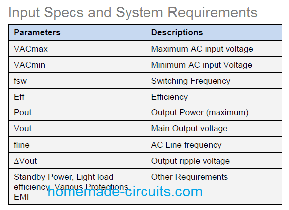
We know that the efficiency parameter is the crucial one that needs to be decided first, the easiest way is to go about is to set a target of around 75% to 80%, even if your design is a low cost design. The switching frequency denoted as
Fsw generally has to be compromised while getting the best of transformer size and losses incurred due to switching, and EMI. Which implies one may need to decide on a switching frequency at least below 150kHz. Typically this may be selected between a 50kHz and 100kHz range.
Furthermore, in case more than one output is required to be included for the design, the maximum power value Pout will need to be adjusted as the combined value of the two outputs.
You may find interesting to know that until recent times the most popular conventional SMPS designs used to have the mosfet and the PWM switching controller as two different isolated stages, integrated together over a PCB layout, but nowadays in modern SMPS units these two stages can be found embedded inside one package and manufactured as single ICs.
Mainly, the parameters which are typically considered while designing a flyback SMPS converter are 1) The application or the load specifications, 2) Cost 3) Standby power, and 4) Additional protection features.
When embedded ICs are used, usually things become a lot easier, as it only requires the transformer and a few external passive component to be calculated for designing an optimal flyback converter.
Let’s get into the details regarding the involved calculations for designing a flaback SMPS.
Calculating the Input Capacitor Cin, and the Input DC Voltage Range
Depending on input voltage and power specifications, the standard rule for selecting Cin which is also referred to as a DC link capacitor can be learned from the following explanations:

In order to ensure a broad range of operation, a 2uF per watt or higher value may be chosen for a DC link capacitor, which will enable you to have a good quality range for this component.
Next, it may be required to determine the minimum DC input voltage which may be obtained by solving:

Where the discharge becomes the duty ratio of the DC link capacitor, which may be roughly around 0.2
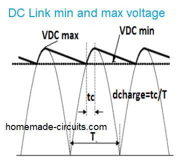
In the figure above we can visualize the DC link capacitor voltage. As shown, the input voltage arises during maximum output power and minimum input AC voltage, whereas the maximum DC input voltage arises during minimum input power (absence of load) and during maximum input AC voltage.
During no load condition, we are able to see a maximum DC input voltage, during which the capacitor charges at the peak level of the AC input voltage, and these values can be expressed with the following equation:

Step3:
Evaluating the Flyback induced voltage VR, and the maximum voltage stress on the MOSFET VDS. The Flyback induced voltage VR could be understood as the voltage induced across the primary side of the transformer when the mosfet Q1 is in switched OFF condition.
The above function in turn impacts maximum VDS rating of the mosfet, which may be confirmed and identified by solving the following equation:

Where, Vspike is the voltage spike generated due to transformer leakage inductance.
To start with, a 30% Vspike out of VDSmax can be taken.
The following list tells us how much reflected voltage or induced voltage may be recommended for a 650V to 800V rated MOSFET, and having an initial limit value VR lower than 100V for an expected vast input voltage range.

Picking the right VR can be a bargain between the level of voltage stress over the secondary rectifier, and the primary side mosfet specifications.
If VR is selected very high through an increased turn ratio, would give rise to a bigger VDSmax, but a lower level of voltage stress on the secondary side diode.
And if VR is selected too small through a smaller turn ratio, would cause VDSmax to be smaller, but would result in an increase in the stress level on the secondary diode.
A bigger primary side VDSmax would assure not only lower stress level on the secondary side diode and reduction in primary current, but will also allow a cost effective design to be implemented.
Flyback with DCM Mode
How to Calculate Dmax depending on Vreflected and Vinmin
A maximum duty cycle can be expected at instances of VDCmin. For this situation we may design the transformer along the thresholds of DCM and CCM. In this case the duty cycle could be presented as:

Step4:
How to Calculate Primary Inductance Current
In this step we will calculate primary inductance and primary peak current.
The following formulas could be used for identifying primary peak current:

Once the above is achieved we can go ahead and calculate the primary inductance using the following formula, within the maximum duty cycle boundaries.

Care must be taken regarding the flyback, it must not go into the CCM mode due to any form of excess loading conditions, and for this maximum power specification should be considered while calculating Poutmax in Equation#5. The mentioned condition can also occur in case inductance is increased over the Lprimax value, so take a note of these.
Step5:
How to Select Optimal Core Grade and Size:
It might look quite intimidating while selecting the right core specification and structure if you are designing a flyback for the first time. Since this may involve a significant number of factors and variables to be considered. A few of these that may be crucial are the core geometry (e.g. EE core/RM core/PQ core etc), the core dimension (eg. EE19, RM8 PQ20 etc), and the core material (eg.3C96. TP4, 3F3 etc).
If you are clueless regarding how to proceed with the above specs, an effective way to counter this problem could be to refer a standard core selection guide by the core manufacturer, or you can also take the help to the following table which roughly gives you the standard core dimensions while designing a 65kHz DCM flyback, with reference to the output power.

Once you are done with the selection of the core size, it is time to select the correct bobbin, which could be acquired as per the core datasheet. Additional properties of the bobbin such as number of pins, PCB mount or SMD, horizontal or vertical positioning all these may also need to be considered as the preferred design
The core material is also crucial and must be selected based on the frequency, magnetic flux density, and core losses.
To begin with you can try variants with the name 3F3, 3C96, or TP4A, remember the names of available core material may be different for identical types depending on the particular manufacture.
How to Calculate Minimum Primary Turns or Winding

Where the term Bmax signifies the operating maximum flux density, Lpri tells you about the primary inductance, Ipri becomes the primary peak current, while Ae identifies the cross sectional area of the selected core type.
It must remembered that the Bmax should never be allowed to exceed the saturating flux density (Bsat) as specified in the datasheet of the core material. You may find slight variances in Bsat for ferrite cores depending on specifications such as material type and temperature; however a majority of these will have a value near to 400mT.
If you find no detailed reference data, you may go with a Bmax of 300mT. Although selecting higher Bmax may assist in having reduced number of primary turns and lower conduction, core loss may significantly increase. Try to optimize between the values of these parameters, such that core loss and copper loss both are kept within acceptable limits.
Step 6:
How to Calculate the number of turns for the main secondary output (Ns) and the miscellaneous auxiliary outputs (Naux)
In order to determine the secondary turns we first need to find the turn ratio (n), which can be calculated using the following formula:

Where Np is the primary turns, and Ns is the secondary number of turns, Vout signifies the output voltage, and VD tells us regarding the voltage drop across the secondary diode.
For calculating the turns for the auxiliary outputs for a desired Vcc value, the following formula can be used:

An auxiliary winding becomes crucial in all flyback converters for supplying the initial start-up supply to the control IC. This supply VCC is normally used for powering the switching IC on the primary side and could be fixed as per the value given in the datasheet of the IC. If the calculation gives a non-integer value, simply round it of by using the upper integer value just above this non integer number.
How to Calculate the wire size for the selected output winding
In order to correctly calculate the wire sizes for the several winding, we first need to find out the RMS current specification for the individual winding.
It may be done with the following formulas:


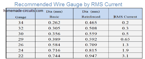
As a starting point, a current density of 150 to 400 circular mil per Ampere, could be utilized for determining the gauge of the wire. The following table shows the reference for selecting the appropriate wire gauge using 200M/A, as per the RMS current value. It also shows you the diameter of the wire and the basic insulation for an assorted gauge of super enameled copper wires.
Step8:
Considering the construction of the transformer and Winding design Iteration
After you have finished determining the above discussed transformer parameters, it becomes crucial to evaluate how to fit the wire dimension and the number of turns within the calculated transformer core size, and the specified bobbin. To get this right optimally several iteration or experimentation may be required for optimizing the core specification with reference to wire gauge and the number of turns.
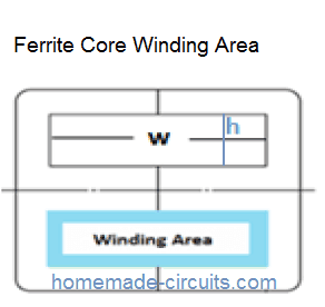
The following figure indicates the winding area for a given EE core. With reference to the calculated wire thickness and the number of turns for the individual winding, it may be possible to approximately estimate whether the winding will fit the available winding area (w and h) or not. If the winding does not accommodate then one of the parameters out of number of turns, wire gauge or the core size, or more than 1 parameter may require some fine-tuning until the winding fits optimally.
The winding layout is crucial since the working performance, and the reliability of the transformer, significantly depends on it. It is recommended to employ a sandwich layout or structure for the winding in order to restrict inductance leakage, as indicated in Fig5.
Also in order to satisfy and conform with the international safety rules, the design must have sufficient range of insulation across the primary and secondary layers of winding. This may be assured by employing margin-wound structure, or by using a secondary wire having triple insulated wire rating, as shown in the following respective figure

Employing triple insulated wire for the secondary winding becomes the easier option for quickly affirming the international safety laws concerning flyback SMPS designs. However such reinforced wires may have a bit higher thickness compared to the normal variant compelling the winding to occupy more space, and may require additional effort to accommodate within the selected bobbin.
Step 9
How to design the Primary Clamp Circuit
In the switching sequence, for the OFF periods of the mosfet, a high voltage spike in the form of leakage inductance is subjected across the mosfet drain/source, which might result in an avalanche breakdown, ultimately damaging the mosfet.
To counter this a clamping circuit is usually configured across the primary winding, which instantly limits the generated spike to some safe lower value.
You will find a couple of clamping circuit designs that may be incorporated for this purpose as shown in the following figure.
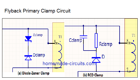
These are namely RCD clamp, and Diode/Zener clamp, where the latter is much easier to configure and implement than the first option. In this clamp circuit we use a combination of a rectifier diode and a high voltage Zener diode such as a TVS (transient voltage suppressor) for clamping the surge spike.
The function of the Zener diode is to efficiently clip or limit the voltage spike until the leakage voltage is fully shunted through the Zener diode. The advantage of a diode Zener clamp is that the circuit activates and clamps only when the combined value of VR and Vspike exceeds the breakdown spec of the Zener diode, and conversely, as long as the spike is below the Zener breakdown or a safe level, the clamp may not trigger at all, not allowing any unnecessary power dissipation.
How to Select Clamping Diode/Zener Rating
It is should always twice the value of the reflected voltage VR, or the assumed spike voltage.
The rectifier diode should be ultra-fast recovery or a schottky type of diode having a rating higher than the maximum DC link voltage.
The alternative option of RCD type of clamping has the disadvantage of slowing down the MOSFET’s dv/dt. Here the resistance parameter of the resistor becomes crucial while limiting the voltage spike. If a low value Rclamp is selected it would improve the spike protection but might increase dissipation and waste energy. Conversely, if a higher value Rclamp is selected, that would help to minimize dissipation but might not be so effective in suppressing the spikes.
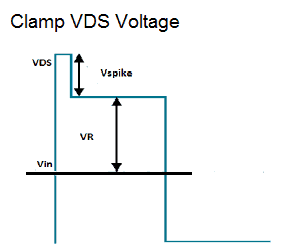
Referring to the figure above, to ensure VR = Vspike, the following formula could be used

Where Lleak signifies the inductance of the transformer, and could be found by making a short circuit across the secondary winding, or alternatively, a rule of thumb value could be incorporated by applying 2 to 4% of the primary inductance value.
In this case the capacitor Cclamp should be substantially large inhibit a rise in voltage during the absorption period of the leakage energy.
The value of Cclamp may be selected between 100pF to 4.7nF, the energy stored inside this capacitor will be discharged and refreshed by Rclamp quickly during eacj switching cycle.
Step10
How to Select Output Rectifier Diode

This may be calculated using the formula shown above.
Make sure to select the specifications such that the maximum reverse voltage or the VRRM of the diode is not less than 30% than the VRVdiode, and also ensure that the IF or the avalanche forward current spec is minimum 50% greater than the IsecRMS. Preferably go for a schottky diode to minimize conduction losses.
With a DCM circuit the Flyback peak current may be high, therefore try selecting a diode having a lower forward voltage and a relatively higher current specs, with regards to the desired efficiency level.
Step11
How to Select the Output Capacitor Value
Selecting a correctly calculated output capacitor while designing a flyback can be extremely crucial, because in a flyback topology stored inductive energy is unavailable between the diode and the capacitor, which implies the capacitor value needs to be calculated by considering 3 important criteria:
1) Capacitance
2) ESR
3) RMS current
The minimum possible value could be identified depending on the function of maximum acceptable peak to peak output ripple voltage, and may be identified through ghe following formula:

Where Ncp signifies the number of primary side clock pulses required by the control feedback for controlling the duty from the specified maximum and minimum values. This may typically require around 10 to 20 switching cycles.
Iout refers to the maximum output current (Iout = Poutmax / Vout).
To identify the maximum RMS value for the output capacitor, use the following formula:

For a specified high switching frequency of the flyback, the maximum peak current from the secondary side of the transformer will generate a correspondingly high ripple voltage, imposed across the equivalent ESR of the output capacitor. Considering this it must be ensured that the ESRmax rating of the capacitor does not exceed the specified acceptable ripple current capability of the capacitor.
The final design may fundamentally include the desired voltage rating, and ripple current capability of the capacitor, based on the actual ratio of the selected output voltage and current of the flyback.

Make sure that the ESR value is determined from the datasheet based on the frequency higher than 1kHz, which may be typically assumed to be between 10kHz to 100kHz.
It would be interesting to note that a solitary capacitor with a low ESR spec may be enough to control the output ripple. You can try to include a small LC filter for higher peak currents, especially if the flyback is designed to work with a DCM mode, which might guarantee a reasonably good ripple voltage control at the output.
Step12
Further Important Considerations:
A) How to Select Voltage and Current rating, for the Primary side Bridge rectifier.

It can be done through the above equation.
In this formula PF stands for power factor of the power supply, we can apply 0.5 in case a proper reference becomes out of reach. For the bridge rectifier select the diodes or the module having a forward amp rating 2 times more than the IACRMS. For the voltage rating, it could be selected at 600V for a maximum 400V AC input specification.
B) How to Select the Current Sense Resistor (Rsense):
It may be calculated with the following equation. The sensing resistor Rsense is incorporated to interpret the maximum power at the output of the flyback. Vcsth value could be determined by referring to the controller IC datasheet, Ip(max) signifies the primary current.

C) Selecting the VCC of the Capacitor:
An optimal capacitance value is crucial for the input capacitor to render a proper startup period. Typically any value between 22uF to 47uF does the job nicely. However if this is selected much lower might result in triggering an “under voltage lockout” on the controller IC, before the Vcc is able to develop by the converter. On the contrary a larger capacitance value could result in an undesirable delaying of the startup time of the converter.
Additionally, make sure this capacitor is of the best quality, having very good ESR and ripple current specifications, on par with the output capacitor specifications. It is strongly recommended to connect another smaller value capacitor in the order of 100nF, parallel to the above discussed capacitor, and as close as possible to the controller IC’s Vcc/ground pinouts.
D) Configuring the Feedback Loop:
Feedback loop compensation becomes important to stop the generation of oscillation. Configuring loop compensation can be simpler for DCM mode flyback than a CCM, due to the absence of “right half plane zero” in the power stage and thus no compensation is called for.
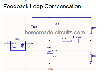
As indicated the above figure a straightforward RC (Rcomp, Ccomp) mostly becomes just enough to maintain good stability across the loop. In general Rcomp value may be selected anything between 1K and 20K, while Ccomp could be within the range of 100nF and 470pF.
This concludes our elaborate discussion on how to design and calculate a flyback converter, if you have any suggestions or questions, you can put them forth in the following comment box, your questions will be replied ASAP.
Courtesy: Infineon

Comments
Hi!
Very interesting.
However, one of the aspects to consider is the effect of winding capacitance? In one home project, I am looking to step up 12V to around 500V, 1W for a small CRT display. However, with very many coils/chokes I am obtaining something well short of voltage required and believe that a simple analysis of the boost converter that does not take into account winding self-capacitance does not gives us the full story?
Any comments/advice please?
Many thanks!
Hi, Thanks, I appreciate your feedback. I will have to investigate the issue to answer your quesiton, I may come back later with an answer.
Could it be that there is an error in calculation of Ip in equation 6. I am quite sure that the factor 2 should be omitted from the formula.
I stand corrected.. I made a flawed assumption and calculated with the maximum current while ignoring that the current in an inductor is sawtooth like. So please forgive my mistaken comments. Equation 6 is correct.
Thank you for your valuable feedback. I appreciate it very much…
Hi we have required a dc to DC converter on flyback topology input range 36 to 100vdc and output is 12v 10A so plz prive and how to design kindly guid me plz resolved this issue which ic select and other parameter
Hi,
I am doing a project on having 3 outputs 12V, 5V, 3.3V. Output power total on 120W too.
Am i able to use the same controllers and devices, since the output is 120W and input voltage are the same.
Just by configuring the winding of transformer will enable me to have 3 different output?
And yes i am doing a flyback application too.
Hi, yes you can configure the output winding to get the 3 outputs using the same circuit.
Hi sir,
i how to select power conversion Topologies, what are the parameter have to consider to select isolated power conversion topologies, e.g flyback, forward ,push-pull, half bridge and full bridge.
please tell some technical parameters
Hi Palani,
there can be many parameters, and the explanation can be too long, it cannot be explained in the comment section.
dear sir! i ‘m facing a little problem with my flyback smps whose output secondry power is 85watt , Vout-dc = 14vdc, Iout -dc = 7ampere-dc approximatly using Nprim = 38turn (swg26 x 3) & Nsec = 5turn (swg26 x 6) & Naux = 5T(swg26 x 6). what should i do with primary turns or secondry turns? to increase its power to output 140watt mean Vout = 14vdc, Iout = 10ampere-dc
Hi Sheraz, you can try using a thicker wire for the transformer secondary, to increase the current output, or alternatively you can add more number of wire strands in parallel for the winding. If upgrading secondary side does not help, you can try the same for the primary side winding also.
sir thanks for replying.
i tried to increase the output current by increasing more wire strands in parallel from (swg 26 x 6) to (swg 26 x 15) but still the result is same. however i did’t try it with primary to add more wire strands i will try it.
Sure, you can try it and see if that works!
Hi, i love your tutorial on smps. Pls can you make a video on this subject for better comprehension. Thank you
I am glad you liked this tutorial. If I get time I will surely try to make a video on this subject!
hello sir,
I have a question, and it is related to flyback converter. I am planning to build a converter that takes 10 to 1000 v DC and converts it to 5 v and 2 a dc . Is it possible to do with Flyback ? which conduction mode should I select ? DCM or CCM ?
Best regards
Mohammad
Hello Muhammad, You can create any type of converter as per your specifications using a flyback topology. CCM, and DCM both have their own merits and demerits so you can select any one of them as per your choice. The advantages and disadvantage of the two modes are given in the following chart:
https://www.homemade-circuits.com/wp-content/uploads/2018/06/3.png
Please can you enlight me on how to design 100w +/-15v using Uc3842
please is it the same way we are going to wind transformer with +/- output voltage
I did not understand your question!
Hi Swagatam,
I love the article you post on this website, and learned a lot from it.
These days I am looking for a power supply unit for a automation product for farmer (a GSM based tubewell monitoring system). This module require power supply of approx 2.5 A (with voltage range of 5-12V, any voltage in between will work). I evaluated many power supply unit available in market – from local as well as well known company, although these supply units are rated for 3A but none give 3A, all fails beyond 2A.
Since this product is for farmer community and I will be giving it to them on non profit basis, my budget for this power supply unit is limited to Rs 300.
I am reaching out to you to help me in identifying any readily available power supply unit, or help in designing it using locally available components with maximum budget of Rs 300.
I hope to get help from you in figuring out the power supply unit.
If possible share your number with me on my email, so that I can reach out to you to share more information about the project.
Thanks,
Shiv
Hi Shiv,
It can be difficult to judge the actual current rating an SMPS without a practical testing, because none of the existing brands have reputed names. However getting a good quality 5 V 3 amp at Rs.300 can be very difficult. The nearest that I could find is 5 V 5 amp at Rs. 348 from amazon. Maybe buying in quantity can reduce the price to Rs. 300.
If you buy a 5 amp SMPS then you can get a guaranteed 3 amp from it.
Building it yourself can be even more expensive and unreliable, therefore I suggest buying the above mentioned option, either online or from a retailer.
The ones that have metal net like cover appear to be more sturdy and of better quality than the ones plastic cover
Please feel free to discuss the project here through comments, I will be happy to help!
Thanks Swagatam sir for quick reply and your valuable suggestion. Metal cover SMPS is not an option because of its size.
Please share the Amazon link of one that you suggested in your comment.
Thank you Shiv, the amazon smps which I suggested has a metal cover, so it might not be suitable for you.
You can find it with the following search phrase:
Easy Electronics 5 Volt 5 Amp DC Power Supply SMPS (5V 5A)
If anyone is interested in going into a bit more depth : https://www.ti.com/seclit/ml/slup338/slup338.pdf.
One of the contributors, Colin Gillmor, is a long-time friend.
What are the advantages & disadvantages of using a split-bobbin in flyback transformer ?
I have plenty of physical space for a heavily insulated, stranded conductor, for primary and secondary. There is no feedback winding.
I don’t see any technical advantage or disadvantage between a normal bobbin and a split bobbin, Split bobbins probably only allows winding two sets of coils separately and more compactly, rather than piling up the two winding one above the other.
From a digital electronics engineer, making my first foray into PSU (battery charger design), a very useful article. Thanks.
Thank you very much for your honest feedback! Glad you liked it!
Dear sir,
I have purchased a smps module, the photo and schematic diagram are in following link
https://www.homemade-circuits.com/wp-content/uploads/2020/05/4-amp-smps-circuit.jpg
this module is said to deliver 4 amps current but delivering only 1.5 amp current above which it switches off. can you please suggest me from the schematic where exactly the current control is being operated and what modification needed to get 4 amp current
with regards
Raveesh
Hi Raveesh, please try altering the value of 0.33 ohm resistor at the source pin of the MOSFET and see if that improves the results, do it slowly and step wise, and make sure to use a 100 watt bulb in series while testing the result.
I tried with two 1 ohm 1 watt resistors parallel to .33 ohms resistor (net resistance .18 ohms) still no improvement in output current. I replaced mosfet with new one(same number) and there is no improvement. From outside verification of Ferrite transformer the secondary winding is having 5 strands of quite thick gauge wire and primary is also quite thick wire. Is there anything else to be tweaked. Hope your website viewers facing this type of problem may throw some light.
with regards
Raveesh
The 0.33 ohm is specifically responsible for controlling the output current so altering it should make the difference. The voltage developed across this resistor is causing the pin6 of the IC to activate and shut down the output. Try shorting this resistor entirely and check whether it helps to improve the current or not, also try removing the 10 ohm MOSFET gate/ground resistor, because I did not find this resistor in the original datasheet diagram of this IC.
Hi Swag,
you are a great electronics expert.
Wow! And amazing smps expert too!
I have a smps from Epson printer, output 42V 0,4A.
Can I modify it to output 12v only changing feedback Zener diodes?
At this moment there are 7 Zener diodes of 6V to get 42V. Can I use only 2 Zener diodes of 6V to output 12V?
How can I send to you attached files? (Photo of smps and electrical scheme in pdf format at page 107 of Epson C67/C68/D68 Service Manual printer).
Thank you very much
Aldo Alessi
from Italy
Hi Aldo, yes you can try replacing the 42 v zener with 12 v, I have already posted an article which addresses a similar topic, you can find it here:
https://www.homemade-circuits.com/how-to-make-variable-current-smps/
the opto feedback section is mostly identical in all smps units
Hi Swagatam,
this is electrical schematic:
https://www.facebook.com/1634453815/posts/10219959745697375/
Do you confirm to me that I only need to change Zener diodes to get wished voltage output?
Thanks very much!
Hi Aldo, if the secondary winding is capable of generating more than 42V then the zener application should work, so make sure the secondary winding is designed to generate more than 42 V.
But I would like get 9V or 12V output.
Why do I have to be sure if secondary winding is capable of generating more than 42V?
Thank you very much!!!
Hi Swagatam,
here is electrical schematics in pdf format at full resolution of smps which I would modify, by substituting the no.7 of 6V zener diodes with no.2, to get 12V output (at page 107):
https://www.homemade-circuits.com/wp-content/uploads/2020/06/42V-smps.jpg
Then, I ask to you what’s the task of PSC pin in electrical schematic (output)?
Is it significant for output voltage/current regulation?
Thank you very much!
Aldo
Hi Aldo,
sorry I can’t understand the real function of the PSC output, but It is not significant for any regulation externally.
Output voltage is regulated by the zeners, and current by R12.
Hi Swagatam,
thank you for your reply.
Then, I ask to you what’s the task of PSC pin in electrical schematic (output)?
Is it significant for output voltage/current regulation?
Thank you very much!
Hello Aldo, your diagram looks extremely faded and blurred, I cannot see anything in it properly.
sorry i got confused, from the image i thought you trying to get 42V……..for 12V it’s just the zener that needs to be changed.
Thanks for sharing your ferrite knowledge.
That is the best article web from many web that I seek for many time.
Good evening sir
Please i whould have love to see a complate circuit diagram base on this topic because what I’m seeing here is pure theory no practical diagram. Thanks
Hi Emma, If it’s possible I’ll try to update the data in the above post…
good day Sir… thanks for helping me…is possible to build AVR?
Good day Sunshine, yes it may be possible.