The following article which discusses a 300 watt pure sine wave inverter circuit with automatic output voltage correction, is a modified version of one of my previous posts, and was submitted to me by Mr. Marcelin. I have explained more about the converter implementations.
The Design
The idea was inspired by the design presented in this article by me, however Mr.Marcelin has refined it considerably for better efficiency and reliability.
To me, the modifications and the implementations done look great and feasible.
So I have explained the design elaborately with the following points:
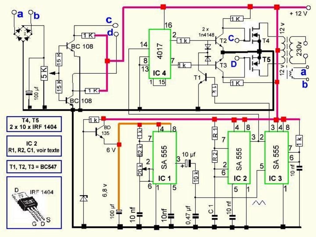
IC2 and IC3 are specifically configured as the PWM generator stage.
IC2 forms the high frequency generator required for pulsing the PWM waveform which is processed by IC3.
For processing the IC2 pulses, IC3 needs to be fed with a sine wave equivalent information at its pin#5, or the control input.
Since creating sine waveform is a bit complex than a triangular waves, the later was preferred as its easier to make yet performs as good as a sine waveform counterpart.
IC1 is wired up as the triangular wave generator, whose output is finally fed to pin#5 of IC3 for the generating the required RMS sine equivalent at its pin#3.
However the above processed PWM signals needs to be modulated over a push-pull kind of arrangement so that the waveforms are able to load the transformer with alternately conducting current.
This is necessary for achieving an output mains consisting of both positive and the negative half cycles.
Circuit Operation
The IC 4017 is introduced just for implementing this action.
The IC generates a sequentially running output from its pin#2 to pin#4, to pin #7, to pin#3 and back again to pin#2, in response to every rising pulse edge at pin #14.
This pulse is derived from the output of IC2, which is set to 200 Hz strictly so that the outputs of IC4017 results in a 50 Hz across the sequencing from the above discussed pin outs.
Pin#4 and pin#3 are purposely skipped, for generating a dead time across the gates triggers of the respective transistors/mosfets connected to the relevant outputs of IC4017.
This dead time makes sure that the devices never conduct together even for a nano second at transition zones, and thus safeguard the health of the devices.
The sequencing positive outputs at pin#2 and 7 trigger the respective devices which in turn force the transformer to saturate with the alternating battery power induced in the respective winding.
This results in the generation of around 330+ V AC at the output of the transformer.
However this voltage would be a square wave with high RMS if it wouldn't be processed with the PWM from IC3.
Transistor T1 along with its collector diode is fed with the PWM pulses such that T1 now conducts and grounds the base trigger voltages of the outputs devices in accordance with the PWM content.
This results in an output that's an exact replica of the the fed PWM optimized input..... creating a perfectly carved pure sine wave AC equivalent.
The circuit has additional features such as a manual output voltage correction circuit.
The two BC108 transistors are stationed for controlling the gate drive voltage levels of the mosfets, the base current of these transistors are derived from a small sensing winding on the transformer which provides the required output voltage level information to the transistors.
If the output voltage goes beyond the expected safe level, the base current of the above transistors may be adjusted and reduced by varying the 5K preset, this in turn brings down the conduction of the mosfets, ultimately correcting the output AC to the required limits.
The BD135 transistor along with its base zener provides a stabilized voltage to the associated electronics for sustaining constant PWM output from the relevant ICs.
With IRF1404 as the mosfets, the inverter would be able to generate anywher around 300 to 5000 watts of pure sine wave output.
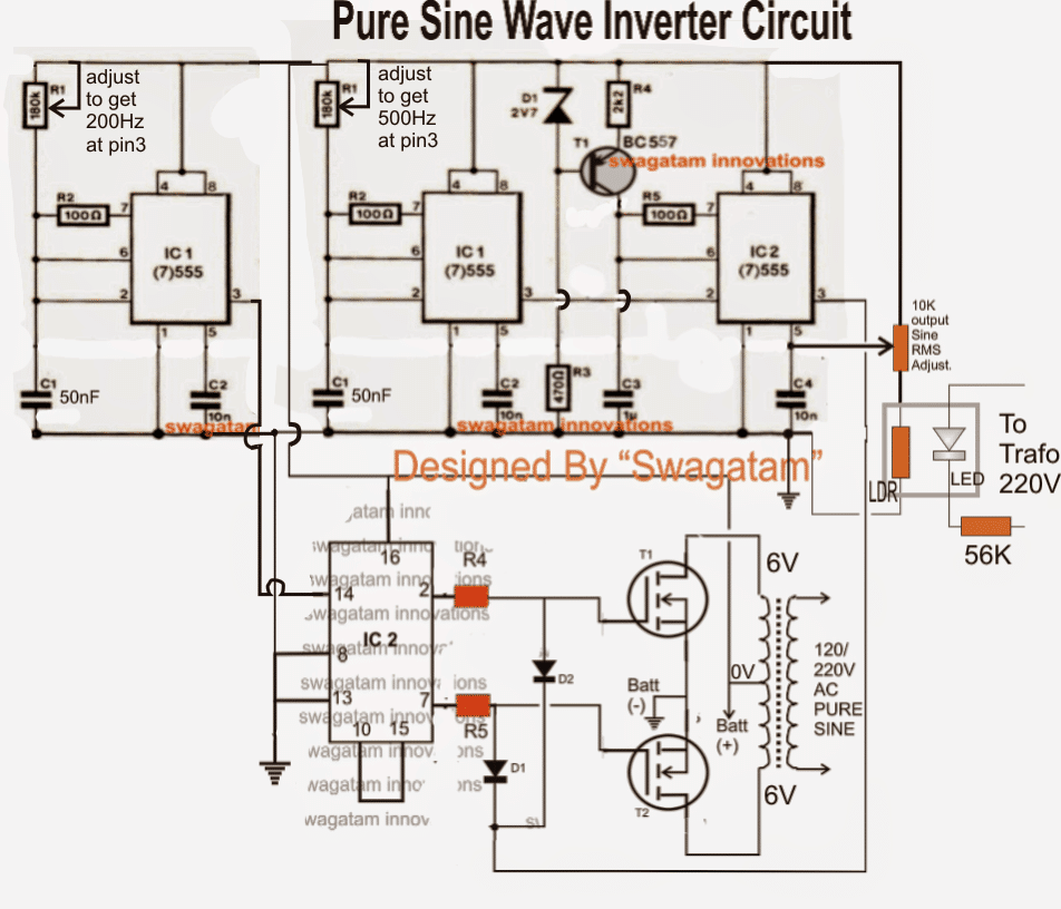
Many drawbacks and flaws were detected while assessing the above circuit details. The finalized circuit (hopefully) is presented below.
The above circuit may be further enhanced with an automatic load correction feature as shown below. It is implemented by the inclusion of the LED/LDR opto-coupler stage.
For the final verified design of the above circuit please refer to the following post:https://www.homemade-circuits.com/2013/10/modified-sine-wave-inverter-circuit.html

Comments (122)
Hi
I am trying to solve a problem created by Ripple Control Modulation by the power authorities… as this is not present where in the region where I live (Western Australia), I need to develop my own Ripple Control Voltage Generator with a the 220-240VAC 50HZ RMS output which is ripple modulated by single individually selectable frequencies, 1050Hz, 750Hz, 462Hz or 283Hz … there may be one or two lower frequencies still as the power authorities keep changing their modulation frequencies in different regions at various Modulation levels (m index) 20%, 30% or 40%. at the moment I use a Rigol Signal Generator and a modulated 50Hz sine wave at 20Vp-p out and the internal AM Modulation feature. This is useful in testing the filter characteristics but it does not drive the filter at the operating voltage and I know that there are resonance points that create singing noise in the filter when tested live on 240VAC at my friends house. (He lives in a region 3000KM from me where they use this Ripple Control for Street Lighting, Load Shedding and Hot Water System Control regularly) I need to have it at my home to look at developing this for him.
I have tried various Transformer options for isolating the Mains and adding the modulated signal by inductive coupling and X2 Capacitive coupling but I just cannot get enough out of the generator (even with an amplifier to create the 30% or 40%modulation level. The 50Kz simply swamps the modulated input and I have to use an small isolating transformer not to damage my signal generator
I hope you can suggest a workable solution
I look forward to your reply
As I mentioned earlier I reside in Australia (Western Australia), my friend resides in Queensland but am away in Europe at the moment so I may not replay as quickly…
Thank You
Kind regards
Henry
Hi, The concept of ripple control modulation is new to me, and I am not familiar with its working. I do not have the necessary information or the circuit idea for this concept at this time. However, I will try to investigate it, if I happen to find anything interesting will surely notify you about the same.
Please Sir could it be possible to build pure sine wave inverter like the mains one without arduino?
Lawal, you can try the following design, it will provide almost a pure sine waveform at the output.
https://www.homemade-circuits.com/1500-watt-pwm-sinewave-inverter-circuit/
hello sir i need favour from you i need 300watt pure sine wave inverter with cut off voltage using arduino and mosfet kindly i have less time in my project i will be very thankful to you i need your whatsapp number also thanks
mirmurtaza, you can try the following concept:
https://www.homemade-circuits.com/arduino-pure-sine-wave-inverter-circuit/
is 6V on transformer RMS value or peak-peak.
RMS value
Good evening, you have an inverter circuit to have 115 volts to 400 hz three-phase power about 100 watts.
Thank you
Greetings
Giuliano
Hi, yes you can try the designs presented in the following links:
https://www.homemade-circuits.com/three-phase-inverter-circuit/
Sir I’m really need your help in getting
The value of R1,R2 and C1 on the first inverter circuit
Because no value is indicated
Can only see voir texte on the left coner of the diagram
Thank you sir
Hope to hear from you soon
Hi Lord, That will need to be confirmed using a frequency meter and by gradual adjustment of the relevant presets in a practical set up. Calculating it here may not be appropriate, since a practical confirmation would help you to achieve a better and a foolproof accuracy.
Hi swagatam, if the 220vac output of the above second diagram is connected to the standing or ceiling fan, will the standing or ceiling fan make hum noise? If yes, what to do to eliminate the noise with the same diagram? Then will the rotational speed of the fans will be the same as that of sine wave?
Ismail, from Nigeria.
Hi Ismail, as far as I know, connecting a high voltage capacitor such as a 0.22uF/400V across the trafo output wire helps to reduce the hum, this could be further improved with a series inductor.
ok, thank you, sir… i am on working this circuit, hope it will work as desired 🙂 …
hi, sir…
what the function of C3 on the Collector TR3 and how much of its value????
100 ohms will do
and.. the resistor to the gate, what the value should i used for ??
it can be a 1uF/25V capacitor
Hi hui, it helps to genearte the required triangle waves for the IC2 and for the final PWMs
Sorry mr swagatam, suppose i need 25kva as an output of my inverter, what requirements do i need to make 25000watts as an output power
use more mosfets in parallel and upgrade the transformer to 3kva power……
It will happen if either the transformer wattage or the battery AH is not sufficiently rated for handling the load…
hi sir is the schematic already 300 watts?
Hi Jeremy, for achieving 300 watts the trafo should be rated at 350 watts and the battery at around 100 AH
Hi sir,
Pls help, I build an inverter using IC 3524 the inverter is working fine on some appliances but won't work well with a small fan, hair clipper and a desktop computer. Pls what can I do to fix this problem.
Thanks in advance
Hi Kolley,
measure the output voltage of the inverter when you connect those loads, if you find the voltage dropping would indicate an inadequate battery current or transformer wattage.
Hi sir,
I build an inverter using ic 3524, the inverter is working fine on some appliance but won't power a small standing fan and a small clipper. Pls what can I do?
Thanks in advance
Hi Kolley, the fan wattage could be beyond the capacity of the inverter power that's why it's not able to move it…you may have to increase the battery AH and/or the transformer amps for upgrading the inverter range
I am developing 3000 W invertor using pwm technique for that I need to design a transformer with 50 hz frequency the resulting transformer is bulki and costlier, I am using 1000 hz pwm frequency for switching, if I design transformer with this frequency the resulting transformer is comparably very small and cheap.
My question is — is that ok to design transformer according to pwm frequency? Please help me out with this problem.
Thanx..
You will need to employ a ferrite core transformer design for fulfilling the design idea.
A 1kHz will not do, you may have require above 20kHz for an efficient response from the ferrite core trafo…and in the next step the output from the ferrite trafo will need to be rectified and converted back to AC at 50Hz frequency in order to make it usable with the normal electrical appliances.
can i use 2pair of irf3205 and 600va ups transformer for 300w inverter ????
yes it can be tried
can i use 600va ups transformer instead of 5A transformer 12-012v for 100w inverter for 90w load ( 1 fan )
yes it can be used.
this will happen if the current from the inverter is not sufficient for the load.
the load sucks more current dropping the voltage.
Sir is there any modification for this circuit to produce the output of 220v at 60hz?
and can i use 12-0-12 2amp transformer?
SIR, are you sure circuit diagram 1 & 2 are pure sine wave (like as MAIN AC)?
waveforms will be pwm based sine wave, equivalent to pure sine wave.
hi sir i finally build this 300 Watts PWM Controlled, Pure Sine Wave Inverter Circuit with Output Voltage Correction but if i power the circuit the two mosfets get very hots without plugin any load its get hots for even 4 to 5 seconds why sir please i need your help thank you im looking forward to hear from you son.
disconnect the transformer from the mosfet and first confirm the frequency inputs at pin14 of IC4017 and pin3 of IC2 555.
pin14 should have a frequency of 200Hz, pin#3 of IC2 should have a frequency of 500Hz.
Once these are confirmed, remove the diode connections from the gate of the mosfets and reconnect the transformer with the mosfet and now check the response from the mosfet and the trafo output. It should work as expected without heating….after this connect the diodes to the gates and check the response again….also keep the load correction removed initially while doing the above tests.
Hi sir thank you for de good job you have provided i pray that god will guide you and give you more knowledge so that you can produce more circuit,sir this300 Watts PWM Controlled, Pure Sine Wave Inverter Circuit with Output Voltage Correction i been study this circuit for about one week,sir i am not too much good in calculation so please i need you to assist me,can i replace 47nf in place of 50nf and100k pot in place of 180kpot? cos its difficult to get it here and also we have only NE555 can it be use thank you i hope to hear from you son/
Hi sir thank you for de good job you have provided i pray that god will guide you and give you more nor rage so that you can produce more circuit,sir this 300 Watts PWM Controlled, Pure Sine Wave Inverter Circuit with Output Voltage Correction i been study this circuit for about one week,sir i am not too much good in calculation so please i need you to assist me,can i replace 47nf in place of 50nf and100k pot in place of 180kpot? cos its difficult to get it here and also we have only NE555 can it be use thank you i hope to hear from you soon
yes ne555 can be used, see previous comment for the remaining answers.
Hi sir thank you for de good job you have provided i pray that god will guide you and give you more nor rage so that you can produce more circuit,sir i been study this circuit for about one week,sir i am not too much good in calculation so please i need you to assist me,can i replace 47nf in place of 50nf and100k pot in place of 180kpot? cos its difficult to get it here and also we have only NE555 can it be use thank you i hope to hear from you son. 300 Watts PWM Controlled, Pure Sine Wave Inverter Circuit with Output Voltage Correction
Hi Biannz,
thanks! instead of 100k you can try using 220K pot that would give you a better range of selection. 47nF can be replaced with 50nF
sir in this circuit 300 Watts PWM Controlled, Pure Sine Wave Inverter Circuit with Output Voltage Correction can bc548 replace bc108 transistor? sir i have search every electronic shops here in my country all they is NE555 they don't have SA555 can i use ne555 without problem? sir in your comment you said pin2 of the IC1 should remove and connect to pin3 of IC4 should we follow that or ignore and build the circuit as it provided? thank you i am waiting for your rply.
zinnaboy the first diagram has many flaws in it so don't try it.
what is the voltage of the battery?
NO, it's a modified sine wave.