In this post I have explained a simple car laptop charger circuit for charging laptops from a 12V car battery using a IC 555 based boost converter. The idea was requested by one of the avid readers of this blog.
Making a 12V to 19V Converter
May I request you for a circuit diagram for a transformerless small 100w inverter which can be used with a car 12V battery to power a laptop? I've found one circuit online but as I am a very new comer to electronics, I didn't understand that. Your help will be highly appreciated. Thanks
You may also like: 12 V to 19 V Converter Circuit
The Transistor Astable Design
A classic boost converter which will perfectly suit the proposed 12 V to 24 V car laptop charger application can be quickly built using a fully transistorized design as shown below:
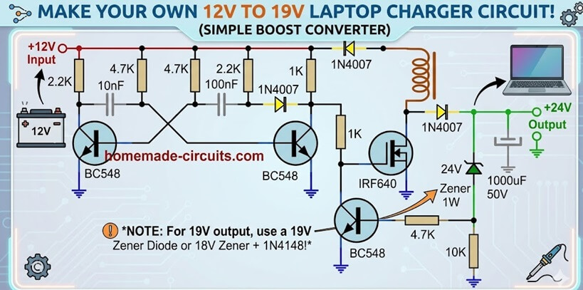
All the shown parts are standard, or could be replaced with other suitable equivalents.
The inductor which is one of main parts of the circuit is built over a ferrite rod 1 cm in diameter, by winding 100 turns of super enameled copper wire having 1 mm thickness.
Actually, the inductor is dependent on the frequency of the transistor astable. For higher frequencies the number of turns will proportionately go down, and is a matter of some experimentation. The turn number will also depend on the ferrite core shape, and may significantly decrease if a ring type ferrite core is used.
Audio/Video Representation
Calculating the Part Values
Astable Multivibrator Section:
The astable multivibrator is designed to generate a square wave to drive the MOSFET. It uses two BC548 transistors with capacitors and resistors which forms the timing network.
Frequency Formula:
- f = 1 / (1.44 * (R1 + 2R2) * C)
Here: - R1 = 2.2k ohms (astable feedback resistors)
- R2 = 4.7k ohms (base resistors)
- C = 10 nF
- Calculations:
- f = 1 / (1.44 * (2200 + (2 * 4700)) * 10 * 10-9)
- f = 1 / (1.44 * 11600 * 10-8)
- f ≈ 6.06 kHz
- Thus the switching frequency of the square wave is approximately 6.06 kHz.
- MOSFET Boost Converter Stage:
- The IRF640 MOSFET switches the inductor to step up the voltage.
- Inductor Value (L):
- The inductor value depends on the peak current (Ipeak), duty cycle (D), and switching frequency (f).
- The output voltage (Vout) is determined by:
- Vout = Vin / (1 - D)
For Vin = 12 V and Vout = 24 V, the duty cycle is: - D = 1 - (Vin / Vout)
- D = 1 - (12 / 24) = 0.5 (50 percent)
The inductor value is calculated using: - L = (Vin * D) / (f * ΔI)
Assume ΔI = 20 percent of Iload, where Iload = Pout / Vout. - For Pout = 20 W:
- Iload = 20 / 24 ≈ 0.84 A
Peak-to-peak ripple current: - ΔI = 0.2 * 0.84 = 0.168 A
- Now calculate L:
- L = (12 * 0.5) / (6060 * 0.168) = 0.005893 Henry
- L ≈ 5.893 mH
We will choose a standard inductor value of 6 mH. - Output Capacitor (Cout):
- The output capacitor filters the ripple voltage.
- Cout = (Iload * D) / (f * Vripple)
- For general-purpose applications we can take output ripple voltage of 1-2% of the output voltage.
- For Vout = 24 V
- Vripple ≈ 0.02 * 24 = 0.48 V
- However it is better to assume a smaller ripple such as 50 mV (much less than 2%) which can ensure much tighter output regulation.
So, assume Vripple = 50 mV: - Cout = (0.84 * 0.5) / (6060 * 0.05)
- Cout ≈ 693 μF
Choose a standard capacitor value of 1000 μF, 50V.
Diodes (1N4007):
The diodes must handle the peak current and voltage. The current rating should exceed Ipeak = 0.42 A and the voltage rating should exceed Vout = 24 V.
The 1N4007 diodes (1A, 1000V) meet these requirements.
Feedback Network:
The 24V Zener diode ensures that the output voltage is regulated. It clamps the voltage at 24V to prevent overvoltage. The 4.7k resistor limits the current through the Zener diode.
Final Results:
- Frequency: 6.06 kHz
- Inductor: 6 mH
- Output Capacitor: 1000 μF, 50V
- Diodes: 1N4007
- Zener Diode: 24V, 1W
- Feedback Resistor: 4.7k ohms
The IC 555 Design
The proposed car laptop charger circuit is actually a simply boost converter unit designed for generating the required laptop charging voltage.
A simple boost converter can be made using the IC 555, I probably have discussed it through many other posts in this blog.
As may be witnessed in the following figure, a simple yet very efficient boost converter circuit can be constructed for using with laptops from any high current source having a lower voltage than the laptop charging level.
Circuit Diagram for the Boost Converter
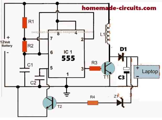
The various stages included in the above 12 V laptop boost charger circuit may be understood as follows:
IC1 which is a 555 IC is configured as a standard astable for generating a stable predetermined frequency at the rate of 12 kHz which is acquired at pin3 of the IC.
The above high frequency output is fed to the base of a driver BJT T1 for inducing the above frequency with high current in L1.
Due to the inherent property of the inductor L1, during every OFF time of T1, an equivalent amount of boosted voltage is kicked back from the inductor L1 and supplied to the load connected at the output via the fast recovery diode BA159.
The load here is the laptop which accepts the boosted voltage for charging its internal battery.
Since the laptop may require a precise 19 to 20V for the operations, the output from L1 must be regulated and stabilized in order to make things safe for the connected laptop battery.
The above criterion is taken care of by introducing T2 and the associated R4 and Z1 components.
Z1 is selected to be exactly equal to the laptop charging voltage that is at 20 V (17V is wrongly shown in the diagram).
Whenever the output tends to drift away from this value, Z1 gets forward biased triggering T2, which in turn grounds pin5 of the IC.
The above situation immediately reduces the IC 555 pin3 voltage to minimal levels for that instant until Z1 stops conducting and the situation is restored to the safe zone....the switching is sustained at a rapid speed maintaining a constant voltage for the laptop.
This car laptop charger circuit can be used for charging a laptop in any car which uses a 12V battery.
Calculating the Part Values
The above 555 circuit is designed to convert 12V DC input to 19V DC output with a current of 2A for charging a laptop.
Output Voltage and Current:
- Input Voltage (Vin): 12V
- Output Voltage (Vout): 19V
- Output Current (Iout): 2A
Inductor Selection (L1):
The inductance is calculated using the formula:
L = (Vin * (1 - D)) / (f * ΔI)
Where:
- Vin = 12V (input voltage)
- D = (Vout - Vin) / Vout = Duty cycle
- Vout = 19V (output voltage)
- f = 50 kHz = 50,000 Hz (switching frequency of the 555 timer)
- ΔI = 20% of Iout = 0.2 * 2 = 0.4A (ripple current)
Step 1: Calculate Duty Cycle (D):
D = (19 - 12) / 19 = 7 / 19 ≈ 0.37
Step 2: Calculate Inductance (L):
L = (Vin * (1 - D)) / (f * ΔI)
L = (12 * (1 - 0.37)) / (50,000 * 0.4)
L = (12 * 0.63) / 20,000
L = 7.56 / 20,000 = 0.000378 H = 378 µH
Inductor Value: 378 µH
Output Capacitor (C3):
The output capacitor filters the ripple voltage. Use the formula:
Cout = (Iout * D) / (f * ΔVout)
Where:
- Iout = 2A
- D = 0.37
- f = 50,000 Hz
- ΔVout = 0.05V (assume 50mV ripple)
Cout = (2 * 0.37) / (50,000 * 0.05)
Cout = 0.74 / 2,500 = 0.000296 F = 296 µF
Capacitor Value: 296 µF (choose a standard value of 330 µF, rated at 25V or higher)
Feedback Zener Diode (Z1):
The Zener diode regulates the output voltage to 19V.
Zener Diode Value:
- Breakdown Voltage: 19V
- Power Rating: Pz = Ifeedback * Vz = 0.01A * 19V = 0.19W
Choose a Zener diode rated at 19V, 0.5W.
Base Resistor for Transistor T2 (R4):
The resistor R4 controls the base current of T2. Use the formula:
R4 = (Vout - VBE) / IB
Where:
- Vout = 19V
- VBE = 0.7V
- IB = Iout / hFE, assuming hFE = 100 (gain of T2)
Step 1: Calculate Base Current (IB):
Since IC555 pin#5 is a high impedance input, just a 10mA current would be enough to sink by T4 collector, so we can select Iout = 10 mA
IB = Iout / hFE = 0.01 / 100 = 0.02A
Step 2: Calculate R4 Value:
R3 = (19 - 0.7) / 0.0001
R3 = 183000 Ω or simply, 180 kΩ
Base Resistor for Transistor T1 (R3):
The resistor R3 controls the base current of T1. Use the formula:
R3 = (Vout - VBE) / IB
Where:
- Vout = 19V
- VBE = 0.7V
- IB = Iout / hFE, assuming hFE = 100 (gain of T1)
Step 1: Calculate Base Current (IB):
IB = Iout / hFE = 2 / 100 = 0.02A
Step 2: Calculate R3:
R3 = (19 - 0.7) / 0.02
R3 = 18.3 / 0.02 = 915 Ω
Resistor Value: 915 Ω (choose a standard value of 1 kΩ)
Final Component Values for the Boost Converter Stage:
- Inductor (L1): 378 µH
- Output Capacitor (C3): 330 µF, 25V
- Zener Diode (Z1): 19V, 0.5W
- Current-Sense Resistor (R4): 180 kΩ 1/4 watt
- Base Resistor (R3): 1 kΩ 1/4 watt
Calculating IC 555 Part Values
Now let use calculate the IC 555 astable circuit so that it becomes compatible with the above calculated boost converter parameters.
Main Calculations for R1, R2, and C1 in the 555 Timer Astable Circuit:
Our specific goal is to design the 555 astable circuit to operate at a frequency of 50 kHz with a duty cycle of 37% for the intended boost converter configuration.
Formulas:
- Frequency: f = 1.44 / ((R1 + 2R2) * C1)
- Duty Cycle: D = ((R1 + R2) / (R1 + 2R2)) * 100%
Data for satisfying the boost conversion:
- Desired Frequency (f): 50,000 Hz
- Duty Cycle (D): 37%
- Assume C1 is = 1 nF (0.000001 F)
Step-by-Step Calculations:
Step 1: Solve for R1 + 2R2 Rearranging the frequency formula: R1 + 2R2 = 1.44 / (f * C1)
Substituting the values: R1 + 2R2 = 1.44 / (50,000 * 0.000000001)
R1 + 2R2 = 1.44 / 0.00005 = 28,800 Ω
Step 2: Solve for R1 and R2 using the Duty Cycle formula
Rearranging the duty cycle formula: (R1 + R2) / (R1 + 2R2) = 0.37
Cross-multiply: R1 + R2 = 0.37 * (R1 + 2R2)
Expand and rearrange: R1 + R2 = 0.37R1 + 0.74R2
Rearrange further: R1 - 0.37R1 = 0.74R2 - R2
0.63R1 = 0.26R2
Solving for R1 in terms of R2:
R1 = (0.26 / 0.63) * R2 = 0.4127R
Step 3: Substitute R1 into R1 + 2R2 = 28,800
Substituting R1 = 0.4127R2: 0.4127R2 + 2R2 = 28,800
Simplifying: 2.4127R2 = 28,800
Solving for R2:
R2 = 28,800 / 2.4127 ≈ 11,940 Ω
Step 4: Calculate R1
R1 = 0.4127 * R2
R1 = 0.4127 * 11,940 ≈ 4,930 Ω
Final Component Values of the Astable 555 Stage:
- R1 = 4.93 kΩ (use standard value: 4.7 kΩ)
- R2 = 11.94 kΩ (use standard value: 12 kΩ)
- C1 = 1 nF
Verification:
Frequency: f = 1.44 / ((R1 + 2R2) * C1)
Substituting values: f = 1.44 / ((4,930 + 2 * 11,940) * 0.000000001)
f = 1.44 / (28,810 * 0.000000001)
f = 50,000 Hz
Duty Cycle = D = ((R1 + R2) / (R1 + 2R2)) * 100%
Substitute values: D = ((4,930 + 11,940) / (4,930 + 2 * 11,940)) * 100%
D = (16,870 / 28,810) * 100% ≈ 37%
So we have now verified the calculations and they are perfectly correct.
Full and Final Parts List
All resistors are 1/4 watt 5% CFR
- R1 = 4.93 kΩ (use standard value: 4.7 kΩ)
- R2 = 11.94 kΩ (use standard value: 12 kΩ)
- R3 = 1 kΩ 1/4 watt
- R4 = 180 kΩ 1/4 watt
- C1 = 1 nF
- C2 = 10nF
- C3 = 330 µF, 25V Electrolytic
- T1 = TIP122
- T2 = BC547
- Z1 = 19V, 1 W zener diode
- L1 = 378 µH, using 1 mm super enameled copper wire (magnet wire), over a 1cm diameter ferrite rod.
Using MOSFET Voltage Doubler Circuit
Nest, I have explained a simple circuit which may be incorporated for charging a laptop while driving in car or some other vehicle. The circuit runs without incorporating an inverter or inductors in its configuration Let's learn more.
Using Voltage Doubler without Inductor
The good thing about this circuit is that it does not rely on an inductor topology for the required actions, making the design simpler, and yet effective.
As we all know a laptop runs using a DC potential from an in built Li-Ion battery just as our cell phones do.
Normally we utilize a AC DC adapter for charging a laptop battery in homes and offices, these adapters are actually SMPS power supplies rated with the required and matching specs of the laptop battery.
However the above power supply units work only with AC supplies, and in places where an AC outlet may be available. These units will not work in places where an AC source is not present such as in cars and other similar vehicles.
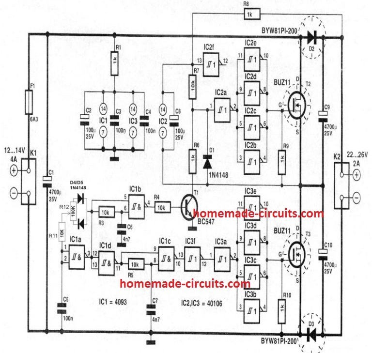
A novel little circuit presented here will allow a laptop battery to be charged even from a DC source such as a car or truck batteries (12V). It's a very simple, cheap, versatile and universal circuit which may be dimensioned for charging all types of laptops by adjusting the relevant components provided in the circuit. It's a simple plug and play charger circuit.
Normally most of the laptop adapters are rated at 19V/3.5Amps, however some may be rated at higher currents for facilitating fast charging.
PWM Charging Control
The discussed circuit has a voltage adjustment features (via PWM) which may be suitably adjusted as per the required specs.
The current may be suitably safeguarded by adding a 3 ohm 5 watt resistor at the output positive terminal.
As can be seen in the circuit diagram, the design is basically a powerful DC to DC voltage doubler circuit which utilizes a push pull mosfet stage for the required boosting of the voltage.
The circuit requires an oscillator stage for initiating the proposed operations which is configured around IC1a.
The components R11, R12, C5 along with the two diodes becomes a neat little PWM controller which sets the duty cycle of the entire circuit and can be used for adjusting the output voltage of the circuit.
Typically the circuit would generate around 22V from a 12V source, by adjusting R12 the output may be tailored to an exact 19V, which is the required laptop charging voltage.



Questions & Answers
A dc dc boost converter uses IC LT1370HVCT7 from linear technologies, i could not find this in markets , any possible substitutes for this? if so please help….
thank you…
sorry no idea about it, you can try the above circuit instead.
can anybody tell me from where should i get the inductor mentioned above please its urgent
just wind 20 to 30 turns using a 20SWG magnet wire over a ferrite rod, that's all your inductor will eb ready…
this is one of the simplest and the most reliable one that you can get, anything simpler than this looks difficult
simulation is not actually necessary for such a simple design, you can simply make it and start using it
sorry I do not have any simulation details because I have not yet simulated it. I have only tested it practically with perfect results
No, Inductances do not have substitutes
which email are you referring to? please click on the diagram and check the out parts list on the right, everything is given there….all the resistors are 1/4 watt rated
I have updated the bridge rectifier circuit at the bottom of the article
sir if we charge our battery by too much high frequency,will not the battery damage???????
A pulsating voltage can actually induce healthy effects on a connected battery….but if you are not sure, you can add a 100uF/25V capacitor after the BA159 diode, which will convert the output to a pure DC
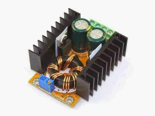
The circuit from the first picture was sold to me as a LED 12V 100W power booster supply. But the LED had a max of 38VCC and the circuit was burning out at 32V.
So now i am study your underwater LED light controller to see if i could get more light out of the LED with that one.
what was exactly burning in the circuit? if it was the capacitors you can change them to 50V specs, anyway thanks for updating the info.
Sir.can I use this circuit to charge a nickel cadmium battery of 9v.I am getting output from the solar panel in a range of 6v.300ma can I able to change this voltage into 9v for charging my nickel cadnium battery.I have one more doubt that how to choose a charging current to charge the nickel casnium type batterybattery.please reply sir
Vijay, yes you can use this circuit for your application, for controlling current you can employ a LM317 circuit and use it in between the solar panel and the above explained boost circuit.
You can use the first design shown in the following article:
https://www.homemade-circuits.com/2013/06/universal-high-watt-led-current-limiter.html
I soldered this ckt but I did not find ba157 in market so I connected general diode 4001. when I connected the ckt to 12 v battery it burrent the tip 122. sir can u tell me the cause of burning of tip122
connect a 1K resistor and a 2200uF/25V across 1N4001 output and ground…if still it burns then the coil could be the one which will need to be examined, and wound again
the diameter of the ferrite rod that I used will be around 15 mm so can I reduce the no of turrens?
initially try with 30 turns and then you can experiment by reducing the turns and simultaneously checking the voltage.
if possible add a current control stage with the TIP as indicated in the following article in order to make the circuit failproof:
https://www.homemade-circuits.com/2015/11/make-this-power-bank-circuit-using-37v.html
Hello Majumdar happy to see this circuit.. as i was making a mini project "solar powered laptop charging" for my school competition..
im using a ups battery for the source which is powered by solar panel..
i need to know that this circuit can be used to charge the laptop from 12v 7.2ah ups battery..
Hello Sanjay, yes this circuit can be used with a 12V 7.2 ah source also….but the coil is crucial and should be experimented correctly to get the most favorable outcome.
Respected sir I connectted 2200uf /25v and 1k across the output I also connected the bc547 and 1 ohm resistor with tip122 as u mansion in the other diagram. Now the output of the ckt is around 11.5 V . I changed the no of turns from 15 to 20 but the output is not increasing.
Zafar, it's simple boost circuit and should work as stated, it will be difficult to troubleshoot your assembly because I can't check it practically.
You can Google "IC 555 boost converter circuit" and see the other online versions, and correct the design accordingly.
read only those circuits which has a coil (inductor), other versions could be useless
The wire gauge is used is 25
gauge is not important, the diameter of the ferrite core and the number of turns are only critical
I soldered this circuit it givese 18.5 V at the output but after a few seconds it heat up the tip122 any solution? I also coconnected 2200uf/25 v dielectric capacitor but still it heating up!
TIP122 may show some heating that's normal, however you can try changing the frequency and see the response.
Replace R1 with a 1M pot and experiment with its adjustment and check the results.
make sure to connect a 10k resistor in series with this pot otherwise your 555 may be at a risk of blowing-off while adjusting the pot.
also make sure to connect a resistor across your 2200uF cap…a 4k7 will do
Zafar can i please have a diagram of your final circuit?
I have connected 1k across 2200 uf
Are there any replacement of tip 122 with high current and voltage ratting?
TIP142 is one transistor that's rated higher than TIP122
you can also try 2N3055
Hi I have successfully adjusted this circuit for 19.5 v output now I m going to connect the charger pin. But the pin have three wires red and black for +ve and -ve and third one I think for sensing its color is white. Where to connect that wire or leave without connecting?
according to me the white wire could be left open and only the red and the black wire considered…..It's better to consult a laptop technician to be entirely sure.
hello sir,
is it possible to acquire an adjustable voltage by replacing Z1 into a 30 volts zener and R4 into a potentiometer?
the output voltage would be 12-30 volts adjustable.
and if T2 will also be change what could be the replacement.
hello jerico, using a pot for R4 will not help to achieve this…a better approach would be to use a pot for R2, and use it as a PWM control and for varying the output voltage
So R2 will be a pot, do I need to increase the no of turns of the inductor to achieve a higher voltage at only 30 volt max?
yes higher coil turns will enable proportionately higher level of voltage
Sir why the voltage drop down from 19.5 to 14 or 15 volts when laptop is connected?
It's due to lack of adequate current….use more parallel wires with the existing coil turns to increase current…or may be the input itself is lacking the required current
Hello sir
Tip 122 transistor heats up for the circuit that I followed as mentioned. And after sometimes it gets damaged. Any solution for it.
did you use a heatink for TIP122?….or you can also try a 2n3055 instead which is more powerful than TIP122
Try connecting a 1k series resistor on the input of the PWM,it helps on reducing the heat of the switch(transistor or mosfet). And heatsink too. I based this on your other circuit that uses PWM.
can you send for me printed circuit of project ? Thank you
very good post..
i should try..
swagatam ji can i salvage one of output filter choke (toroid core) of 450w coputer smps to use as a inductor for the boost charger?
regards
chinmaya
bhubaneswar
thank you chinmaya kumar, yes you can do it, but you may have to manually adjust the number of turns of the inductor with respect to the frequency and duty cycle for getting the most favorable results
hello, the circuit looks really promising on the photo so i tried to simulate it but didnt get any voltage or rather 93 nV which is basically nothing and i did try changing the inductor but that didnt make any difference either.
I really like you post which are very helpful for a newbie like me. It helps me to learn alot.
Thank you.
https://drive.google.com/file/d/0B4EByIot_JMncEV1SVdYc3pZVjQ/view?usp=docslist_api
https://drive.google.com/file/d/0B4EByIot_JMnQlNrLVh0c0wxbWs/view?usp=docslist_api
Hi, The circuit is a standard IC 555 boost converter design so there's no doubt about the configuration, it has to work. I would suggest you to build it practically and check it…I am sure you would be able to get the results instantly, because I could get an instant boost conversion when I tried it. I could boost a 12V source to 80V.
Alternatively you can try removing the BC547 feedback link and see if that helps the situation in your simulator.
Hi, swagatam
i find your site useful alot and i visit it always, thumbs up to you and your good work
please, i want to ask can use a 12 volt @7AH lead acid battery for this project?
Thank you Koby, yes definitely you can use a 12V 7AH battery for the discussed purposed
Sir…how much max current can it supply?
Can I use the same circuit for 19v, 6amp specs?