• Skip to main content
  • Skip to primary sidebar

Homemade Circuit Projects

Need circuit help? Post them in the comments! I've answered over 50,000!

Blog | Categories | About | Hire Me | Contact | Calculators-online
You are here: Home / Battery Charger Circuits / Using MOSFET Body Diodes to Charge Battery in Inverters

Using MOSFET Body Diodes to Charge Battery in Inverters

Last Updated on May 17, 2026 by Swagatam 116 Comments

In this post I have explained how the internal body diodes of MOSFETs could be exploited for enabling the charging of battery through the same transformer which is being used as the inverter transformer.

Table of Contents
  • What is a Full Bridge or H-Bridge Inverter
  • Purpose of MOSFET Internal Body Diodes
    • Using MOSFET Body Diodes for Charging Inverter Battery
    • Basic Working Concept
    • Current Flow Direction through MOSFET Body Diodes
    • Practical Design
  • Relay Changeover Operations

In this article we will investigate a full bridge inverter concept and learn how the in-built diodes of its 4 MOSFETs could be applied for charging an attached battery.

What is a Full Bridge or H-Bridge Inverter

In few of my earlier posts we have discussed full bridge inverter circuits and regarding their working principle.
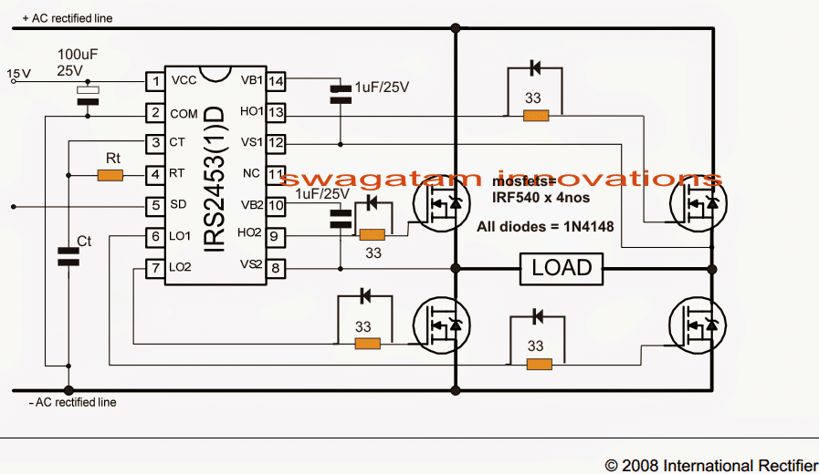
As shown in the above image, basically, in a full-bridge inverter we have a set of 4 MOSFETs connected to the output load. The diagonally connected MOSFET pairs are alternately switched through an external oscillator, causing the input DC from the battery to transform into an alternating current or AC for the load.

The load is normally in the form of a transformer, whose low voltage primary is connected with the MOSFET bridge for the intended DC to AC inversion.

Typically, the 4 N-channel MOSFET based H-bridge topology is applied in full bridge inverters, since this topology provides the most efficient working in terms of compactness to power output ratio.

Although using 4 N channel inverters depend on specialized driver ICs with bootstrapping, yet the efficiency overweighs the complexity, hence these types are popularly employed in all modern full bridge inverters.

Purpose of MOSFET Internal Body Diodes

The internal body diodes present in almost all modern day MOSFETs are primarily introduced to safeguard the device from reverse EMF spikes generated from a connected inductive load, such as a transformer, motor, solenoid etc.

When an inductive load is switched ON through the MOSFET drain, electrical energy gets stored instantaneously inside the load, and during the next moment as the MOSFET turns OFF, this stored EMF is kicked back in the reverse polarity from MOSFET source to drain, causing a permanent damage to the MOSFET.

The presence of an internal body diode across the drain/source of the device thwarts the danger by allowing this back emf spike a direct path through the diode, thus safeguarding the MOSFET from a possible breakdown.

Using MOSFET Body Diodes for Charging Inverter Battery

We know that an inverter is incomplete without a battery, and an inverter battery inevitably requires charging frequently to keep the inverter output topped-up and in the standby condition.

However, charging a battery requires a transformer, which needs to be a high wattage type to ensure optimal current for the battery.

Using a additional transformer in conjunction with the inverter transformer can be quite bulky and costly too. Therefore finding a technique in which the same inverter transformer is applied for charging the battery sounds extremely beneficial.

The presence of the internal body diodes in MOSFETs fortunately makes it possible for the transformer to be switched in the inverter mode and also in the battery charger mode, through some easy relay changeovers sequences.

Basic Working Concept

In the diagram below we can see that, each MOSFET is accompanied with an internal body diode, connected across their drain/source pins.
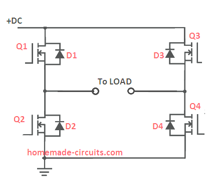
The anode of the diode is connected with the source pin, while the cathode pin is associated with the drain pin of the device. We can also see that since the MOSFETs are configured in a bridged network, the diodes also become configured in a basic full-bridge rectifier network format.

A couple of relays are employed which implement a few quick changeovers for enabling the grid AC to charge the battery via the MOSFET body diodes.

This bridge rectifier network formation of the MOSFET internal diodes actually makes the process of using a single transformer as an inverter transformer and charger transformer very straightforward.

Current Flow Direction through MOSFET Body Diodes

The following image shows the direction of current flow through the body diodes for rectifying the transformer AC to a DC charging voltage
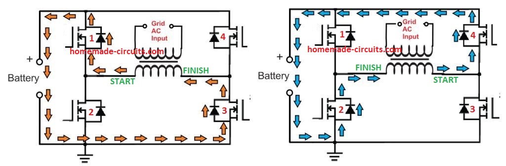
With an AC supply, the transformer wires change their polarity alternately. As shown in the left image, assuming the START as the positive wire, the orange arrows indicate the flow pattern of current via D1, battery, D3 and back to the FINISH or the negative wire of the transformer.

For the next AC cycle, the polarity reverses, and the current moves as indicated by the blue arrows via body diode D4, battery, D2, and back to the FINISH or the negative end of the transformer winding. This keeps repeating alternately, transforming both the AC cycles to DC and charging the battery.

However, since MOSFETs are also involved in the system, extreme care has to be exercised to ensure that these device do not get damaged in the process, and this calls for a perfect inverter/charger changeover operations.

Practical Design

The following diagram shows a practical design set up for implementing MOSFET body diodes as a rectifier for charging an inverter battery, with relay changeover switches.
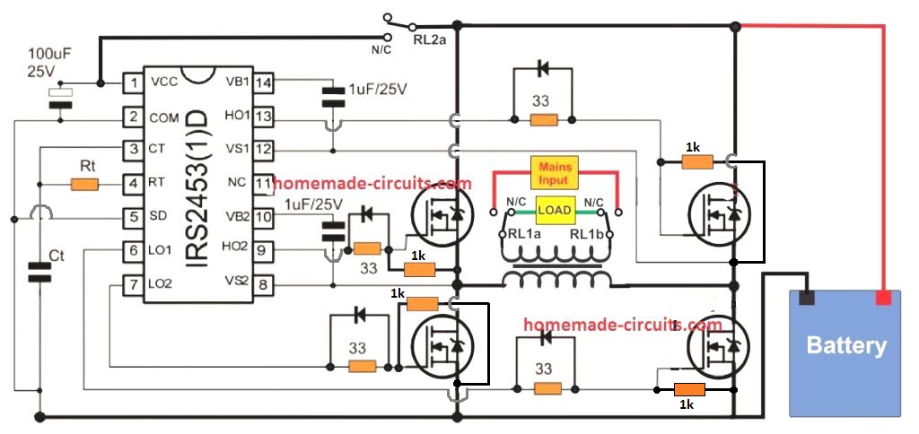
To ensure 100% safety for the MOSFETs in the charging mode and while using the body diodes with the transformer AC, the MOSFET gates must be held at the ground potential, and completely cut-off from the supply DC.

For this we implement two things, connect 1 k resistors across the gate/source pins of all the MOSFETs, and a put a cut-off relay in series with the Vcc supply line of the driver IC.

The cut-off relay is an SPDT relay contact with its N/C contacts connected in series with the driver IC supply input. In the absence of AC mains, the N/C contacts remain active allowing the battery supply to reach the driver IC for powering the MOSFETs.

When mains AC is available, this relay changes over to the N/O contacts cutting off the IC Vcc from the power source, thus ensuring a total cut off for the MOSFETs from the positive drive.

We can see another set of relay contacts connected with the transformer 220 V mains side. This winding constitutes the output 220V side of the inverter. The winding ends are connected with the poles of a DPDT relay, whose N/O an N/C contacts are configured with the mains grid input AC and the load respectively.

In the absence of mains grid AC, the system works in the inverter mode, and the power output is delivered to the load via the N/C contacts of the DPDT.

In the presence of an AC grid input, the relay activates to N/O contacts allowing the grid AC to power the 220V side of the transformer. This in turn energizes the inverter side of the transformer and the current is allowed to pass through the body diodes of the MOSFETs for charging the attached battery.

Before the DPDT relay is able to activate, the SPDT relay is supposed to cut off the Vcc of the driver IC from the supply. This slight delay in activation between the SPDT relay and the DPDT relay must be ensured in order to guarantee 100% safety for the MOSFETs and for the sound operations of the inverter/charging mode via the body diodes.

Relay Changeover Operations

As suggested above, when mains supply is available the Vcc side SPDT relay contact should activate a few milliseconds before the the DPDT relay, at the transformer side. However, when the mains input fails, both the relays must switch OFF almost simultaneously. These conditions could be implemented using the following circuit.
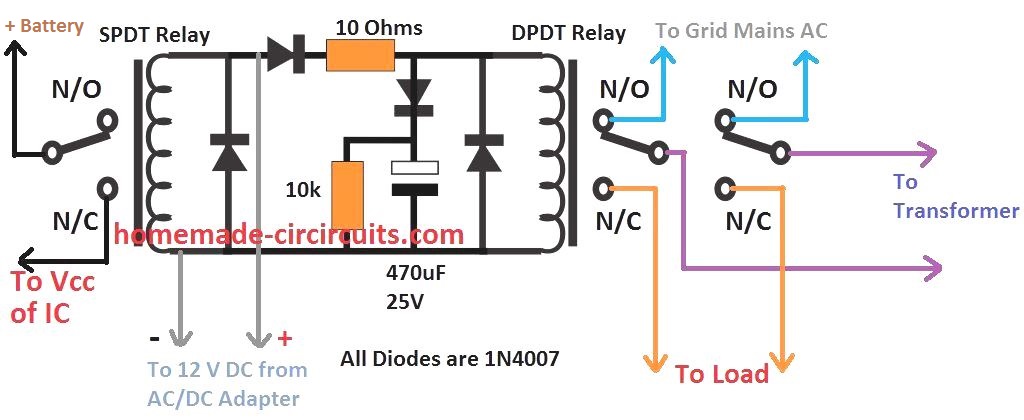
Here, the operational DC supply for the relay coil is acquired from a standard AC to DC adapter, plugged with the grid mains.

This means, when grid AC is available, the AC/DC adapter powers ON the relays. The SPDT relay being connected directly to the DC supply activates quickly before the DPDT relay can. The DPDT relay activates a few milliseconds later due to the presence of the 10 ohm and the 470 uF capacitor. This ensures that the MOSFET driver IC is disabled before the transformer is able to respond to the grid AC input at its 220 V side.

When mains AC fails, both the relay switch OFF almost simultaneously, since the 470uF capacitor now has no effect on the DPDT due to the series reverse biased diode.

This concludes our explanation regarding using MOSFET body diodes for charging an inverter battery through a single common transformer. Hopefully, the idea will allow the many hobbyists to build cheap, compact automatic inverters with built-in battery chargers, using a single common transformer.
You'll also like:

  • Smart Buck-Boost MPPT Solar Charger Circuit for 12V 24V Battery
  • BQ24295 Smart Battery Charger IC with Boost + OTG
  • Fig 1Gel Cell Battery Charger Circuit [Constant Current, Constant Voltage]
  • 4aaacellholderCell Phone Emergency Charger Pack using Ni-Cd Batteries

Filed Under: Battery Charger Circuits Tagged With: Battery, Body, Charge, Diodes, Inverters, MOSFET

About Swagatam

I am an electronics engineer and doing practical hands-on work from more than 15 years now. Building real circuits, testing them and also making PCB layouts by myself. I really love doing all these things like inventing something new, designing electronics and also helping other people like hobby guys who want to make their own cool circuits at home.

And that is the main reason why I started this website homemade-circuits.com, to share different types of circuit ideas..

If you are having any kind of doubt or question related to circuits then just write down your question in the comment box below, I am like always checking, so I guarantee I will reply you for sure!


Previous Post: « Basic Electronic Circuits Explained
Next Post: Stud Finder Circuit – Find Hidden Metals Inside Walls »

Reader Interactions

Questions & Answers

Total Posts: 116
Newest Oldest
David Paul
December 9, 2024 • 2 years ago #166852

hi… swagatam , I have once contributed about this mosfet body diode inverter circuit.here are the research I did about it which give clear explanation on bi-directional inverter with voltage boosting and current regulations when charging and inverting.
my request here is to ask you if you can create an article with schematics for it.
this are the research documentary should I post it here or via your email what’s your email if u decide?

Reply
SwagatamAdmin
December 9, 2024 • 2 years ago #166870

Thank you David,
However I will need a schematic for updating the information. Without a schematic it will be difficult for me to create the article.
If you have done the experiment yourself then please provide the images of the prototype, if possible I will try to figure out the diagram…

Reply
David Paul
December 9, 2024 • 2 years ago #166898

okay, I can draw the circuit related to block diagram but I want you to go through the research I did which can will still make it easy and understanding with that you can create a schematics with reference to the research on chatgpt

Reply
SwagatamAdmin
December 9, 2024 • 2 years ago #166908

I understand your desire to learn more on this subject, however I cannot use chatgpt information to publish on this site, because Google does not like AI based research, Google always prefers practical research based on real human analysis.

Reply
David Paul
December 9, 2024 • 2 years ago #166909

okay then, I will try to sketch out the schematics diagram for you to see it.

Reply
SwagatamAdmin
December 9, 2024 • 2 years ago #166911

That would be great, let me know when it is ready with you….thanks very much for your kind efforts.

Reply
cesar feliz
May 5, 2024 • 2 years ago #151982

Very interesting post… My experience working with inverters (mostly modified sine) has built in chargers and they usually use a triac when the public grid is present. They switch through a CH relay (sometimes use DTDP relays to do this task and transfer), botton line is that triac is controlling a “Chargin tap” in the transforner normally 90VAC tap (fed with 120AC) on a 120AC transformer (double for 220VAC) which increase the charging voltage at Mostef Side. Microcontroller takes care of the 3 stages charging profiles. My question is that I’m building a sine wave inverter with 3 stages charger, the controller is meant to work 12,24,36 and 48vdc depending of some jumpers. I’m using the traditional Triac on charging Tap in the Hivoltage side of the transformer . But my Power board (6KW) it has the snubber circuit and polarizing circuit (resistor and diode) and a 20kohm resistor across gate/source instead the 1kohm as you stated . This 20k resistor will work for the same task of charging (full bridge config is used by this sinewave inverter). Thanks in advance

Reply
SwagatamAdmin
May 5, 2024 • 2 years ago #151993

Hi, thanks for the feedback, and glad you liked the post.
The resistor values across the gate/source of the MOSFFETs is not critical, so a 20k resistor should also be fine. It is simply because MOSFET gates have extremely high impedance in many Megaohms, therefore a 20k will be sufficient enough to hold the gates to the ground level while they are switched OFF.

Reply
cesar feliz
May 5, 2024 • 2 years ago #152010

Perfect. Thanks for your kind reply.

Reply
SwagatamAdmin
May 6, 2024 • 2 years ago #152013

You are welcome…

Reply
James iruero
April 21, 2024 • 2 years ago #151683

Chinonso you cannot increase your output current when charging because input mains is low all you have to do is to design a switching stabilizing unit using a ferosonite system for your inverter mains input

Reply
Chinomso
November 23, 2023 • 3 years ago #147306

Hello Mr. Swagatam. Thank you alot for the illustrations.
I’ve built an hbridge an hbridge inverter of this kind through your professional guidance, the system is working well, fully automatic. However, when in charging mode, and maybe the mains supply is of low voltage, the charging gets stagneted or slows down drastically. Please, is there a way I could include a feedback using autocoupler so as to increase the efficiency of the charging process and also no damage the MOSFETs. Thanks

Reply
cesar feliz
May 5, 2024 • 2 years ago #151985

Most of low frequency inverters (uses 50/60hz transformers) use a charging tap at high voltage side of the inverter (90vac for a 120Vac inverter as reference) . A triac it is used here and controlled by a microcontoller to achive 3 stages charging system , this will boost the voltageat low voltage side of the transformer when main are present and charging is needed.

Reply
SwagatamAdmin
November 23, 2023 • 3 years ago #147311

Hello Chinomso,

A feedback can only help to control an excessive or over voltage situation, a feedback in inverter system are not designed to boost a low voltage situation. So in your case a feedback will not help to increase the charging voltage or efficiency.

Reply
Chinomso
September 25, 2023 • 3 years ago #145422

Your post here Mr. Swagatam,partly answers my previous request for your assistance on MOSFETS dual function of this sort. However sir, my resquest is on a center-tap transformer based inverter. Does this system still applies in my own design?. If not, please what must I do to stop my MOSFETS from blowing up each time I try to charge my batteries. Thanks

Reply
SwagatamAdmin
September 25, 2023 • 3 years ago #145434

Hi Chinomso, Can you please ask this question under the same post where you are having the issue. I will try to help.

Reply
Douglas Powell
August 21, 2023 • 3 years ago #144822

While I agree with this article in principle, I do have concerns.

Using the body diode for higher-power projects is something I typically avoid, mainly for thermal management and EMI. That body diode was optimized for reactive flyback energy within the immediate circuit, in the loads, and not a whole lot more. In my view, the feasibility is not in question, but the practicability is. Very fast diodes are typically used with power MOSFETs. Putting an increased thermal load on the device is not always a great idea. These concerns become all the more important when working with larger systems involving “brick” MOSFET modules, IGBTs, and the newer Power SiC devices.

The use of a full-power diode is especially important in the bi-directional inverters we are now seeing in battery energy storage systems (BESS) that process power in both directions.

Reply
SwagatamAdmin
August 22, 2023 • 3 years ago #144828

Thank you so much for the valuable information. It is much appreciated.

Reply
Hijazi
June 11, 2023 • 3 years ago #143312

Hiii
Dear
How we can adjust and control the voltage and the amperes of these mosfets when we have the batery charger mode…
Please!

Reply
SwagatamAdmin
June 11, 2023 • 3 years ago #143325

Hello, Unfortunately voltage and current cannot be changed in this design. However since the discharge rate of the battery will be the same as the charging rate, so the transformer current will be compatible with the battery.

Reply
David Paul
December 11, 2023 • 3 years ago #147831

Hi… Swagatam
For a 24v 220ah battery the transformer should be able to handle 220amps at inverter mode, then at charging mode the current from the transformer would be extremely high which can destroy the battery.
Charging the battery should be at 1c or 2c (22amps or 30amps).
So how do we bring down the charging current to 22amp or 30amps when the transformer is at charging mode pls i need your help…

Reply
SwagatamAdmin
December 11, 2023 • 3 years ago #147833

Hi David,
A 220 Ah battery can be charged or discharged at 220 amps only if it is a Li-Ion or Li-Po battery.
If it is a lead acid battery or an SMF battery then it must charged and discharged at 0.15 C rate meaning it cannot be charged or discharged over 30 amp rate.
Therefore the transformer must be rated according to the above 30 amp current rating.

Reply
Ben
April 15, 2023 • 3 years ago #141807

Just an observation. Having just repaired a 1000w220vac/ 12vdc inverter charger where the pcb tracks had been severely burnt, replaced 16 mosfets 40v 180amp devices, the primary winding is single 6volt load in the H bridge. The charging waveform is a switched pulse, with the current in the 6volt winding being in excess of 100amps but the initial pulsed charging current into the battery being around 30amps upto 14.8volts at the first rate and reducing to 13.8 volts. The battery used is a 64amphr at the 5hr rate. The charging waveform is not like one would expect from a normal full wave bridge. Each pulse is made up of high frequency pulses.

Reply
IGBINOBA ERERE
March 25, 2023 • 3 years ago #141371

How about in a case of a center taped transformer with just two MOSFET, how do the charging work?

Reply
MORRIS
July 12, 2022 • 4 years ago #131519

Hae sir, I have read it but does the circuit cut off whn the battery reaches the full charge threshold and whn the battery is at the low level? Secondly can I use any MOSFETs like IRF1405 or cs150n03 and instead of four pieces can I connect four in in parallel on each side?

Reply
SwagatamAdmin
July 12, 2022 • 4 years ago #131522

Hi Morris, there is no provision for an automatic cut off in this circuit. You will have to employ opamps for getting this feature.

Yes you can use any desired mosfets provided the power rating is correctly matched with the power of the transformer. You can as many mosfets as you want for increasing its power handling capacity.

Reply
MORRIS
July 15, 2022 • 4 years ago #131600

And is there any using a center tap wire pliz? Secondly, is there any modified sine wave inverter using a two wire without center tap?

Reply
SwagatamAdmin
July 16, 2022 • 4 years ago #131605

Right now I don’t have any of those circuits, if I happen to find one will surely update it for you…

Reply
MORRIS
July 15, 2022 • 4 years ago #131598

How efficient is this body diode inverter compared to the normal ordinary one which u use a separate charger? Secondly I got a power supply with a fixed 12v 12.5amp. Can this charge 200ah battery to the full level threshold despite the more time it will take? Advise, thanks.

Reply
SwagatamAdmin
July 16, 2022 • 4 years ago #131604

I have not it tested the design practically so it can be difficult for me to tell how efficient the design is. A 12V 200 Ah battery will require a minimum of 14 V 20 amp supply, so your power supply cannot be used for charging the battery.

Reply
MORRIS
July 14, 2022 • 4 years ago #131569

But can u check if cs150n03 mosfet can be used in a 24v inverter despite it voltage rating pliz confirm or it’s best suited for 12v inverter

Reply
SwagatamAdmin
July 14, 2022 • 4 years ago #131576

Its VDSS rating is 30V, while a fully charged 24V battery may have a voltage level of 26V which is quite close to 30V so i won’t recommend this mosfet for a 24V inverter. You can try IRF3205 instead.

Reply
Raghu
September 30, 2021 • 5 years ago #98941

Sir what is the Rt value

Reply
SwagatamAdmin
September 30, 2021 • 5 years ago #98947

You can calculate it using the following formula

f = 1/1.453 x Rt x Ct

f is frequency, Ct is capacitor which must be in Farads.

Reply
Aupu
August 10, 2021 • 5 years ago #93798

Thanks for this tutorial. In this schematic, there is no current control for the battery charging. If battery charging current is very high, the battery life will decrease. What should I do to limit the battery charging current?

Reply
SwagatamAdmin
August 10, 2021 • 5 years ago #93805

Yes you are right, the only apparent way to control the input current is by adding a 10uF or 20uF capacitor in series with the Mains Input line connecting the transformer primary, 10uF would limit 500 mA input maisn at 220V, 20uF would limit 1 amp at 220V and so on. This means 9 amp at the battery side at 12 V for 10uF, and 18 amps at 12 V….

Reply
Sherafudheen
February 9, 2021 • 6 years ago #86877

Hi Swagatam,
Can you post boost fpc charging techniques in h bridge inverter for pure sinewave.
This will be very helpful for the new inverter system repair and find out charging issues.

Reply
SwagatamAdmin
February 9, 2021 • 6 years ago #86884

Hi Sherafudheen, Can you please elaborate more on the topic, because I have not yet investigated boost fpc tech, so don’t know much about it at this moment of time!

Reply
Sherafudheen
February 10, 2021 • 6 years ago #86916

In sine wave inverters charging technique is called boost pfc.
In h-bridge configuration during battery charge we shorted lower mosfet with 7 khz pwm signal.
And due to leakage inductance of transformer in 7v winding we can get 13.8v.

Reply
SwagatamAdmin
February 11, 2021 • 6 years ago #86924

OK, thank you! Actually Boost power factor correction is a technology for improving the power factor of the input AC supply using a boost converter inductor.
I don’t think it is specifically used in sine wave inverters.
It can be used in all types of power supplies, inverters, and converters.
Also this may be relevant in online UPS systems where the AC supply is used for charging the battery and also for powering the inverter simultaneously.
In charging concept as above where a MOSFET body diodes are used, using boost PFC can be very difficult, and could make the design too complex!
Anyway, I will try to post one article on boost PFC which is meant for improving the efficiency of a power supply

Reply
Sherafudheen
February 11, 2021 • 6 years ago #86929

Hi Swagatam,
Thanks for your support,
Actually almost new h-bridge sine vawe inverter the primary voltage is 6 to 7 volts for the 12 volts system.
So when we supply 240volts to secondary for charging thr volts will be below 12 volts and not possible to charge the battery?
In this case what we can do?

Reply
Josh
June 20, 2024 • 2 years ago #153119

Hello, I am actually looking for solution to this problem. In a 12v inverter, a 7v-220v transformer is often used. If you apply 220v AC mains, the voltage at the mosfet side will be 6v, which is not enough to charge a 12v battery. I have also read it online that the boost Pfc method is used to boost the voltage. But I can’t find any circuit anywhere.

Pls help.

Reply
SwagatamAdmin
February 11, 2021 • 6 years ago #86943

You are welcome Sherafudheen,
Yes I understand, the boost converter boosts the lower voltage from the transformer upto the battery charging level, since in PWM circuits, the transformer primary is rated lower than the battery, in order to be compatible with the PWM average DC level.

But while using body diodes, adding the boost circuit between the transformer and the battery can be quite complex, I am not sure how this can be done in a simple way…

may be this can be implemented by adding another set of relay contacts…?

Reply
Janardhan Bhat
January 2, 2021 • 6 years ago #85805

I think there is a small correction—cathode is connected to Drain of the Device——–“The anode of the diode is connected with the source pin, while the cathode pin is associated with the source pin of the device. “

Reply
SwagatamAdmin
January 2, 2021 • 6 years ago #85812

Thank you, noted and corrected!

Reply
View Older Comments

Need Help? Please Leave a Comment! We value your input—Kindly keep it relevant to the above topic! Cancel reply

Your email address will not be published. Required fields are marked *

Primary Sidebar


Categories

  • Arduino Projects (95)
  • Audio and Amplifier Projects (134)
  • Automation Projects (18)
  • Automobile Electronics (104)
  • Battery Charger Circuits (90)
  • Datasheets and Components (109)
  • Electronics Theory (150)
  • Energy from Magnets and Earth (41)
  • Games and Sports Projects (11)
  • Grid and 3-Phase (20)
  • Health related Projects (27)
  • Home Electrical Circuits (13)
  • Indicator Circuits (16)
  • Inverter Circuits (98)
  • Lamps and Lights (161)
  • Meters and Testers (72)
  • Mini Projects (28)
  • Motor Controller (68)
  • Oscillator Circuits (30)
  • Pets and Pests (15)
  • Power Supply Circuits (91)
  • Remote Control Circuits (50)
  • Security and Alarm (65)
  • Sensors and Detectors (107)
  • SMPS and Converters (46)
  • Solar Controller Circuits (62)
  • Temperature Controllers (44)
  • Timer and Delay Relay (50)
  • Voltage Control and Protection (44)
  • Water Controller (37)
  • Wireless Circuits (31)


Circuit Simulator

circuit simulator image


Subscribe to get New Circuits in your Email


Other Links

  • Privacy Policy
  • Cookie Policy
  • Disclaimer
  • Copyright
  • Videos
  • Sitemap

People also Search

555 Circuits | 741 Circuits | LM324 Circuits | LM338 Circuits | 4017 Circuits | Ultrasonic Projects | SMPS Projects | Christmas Projects | MOSFETs | Radio Circuits | Laser Circuits | PIR Projects |


Recent Comments

  • Swagatam on Simple Low Dropout Regulator Circuits Explained
  • Swagatam on How to Calculate Transformerless Power Supply Circuits
  • Swagatam on 5 Simple Water Level Controller Circuits
  • Swagatam on Control a Relay ON OFF Using SIM Card, Mobile Phone, and Arduino
  • Louis83 on Control a Relay ON OFF Using SIM Card, Mobile Phone, and Arduino

Social Profiles

  • Twitter
  • YouTube
  • Instagram
  • Pinterest
  • My Facebook-Page
  • Stack Exchange
  • Linkedin

Calculators

  • ZVS Induction Heater + Tank Calculator Tool
  • Zener Diode Calculator
  • Wire Current and Thickness Calculator (Ampacity Calculator)
  • Voltage Divider Calculator
  • Transistor Base Resistor Calculator
  • Transistor Astable Multivibrator Calculator
  • TL431 Calculator
  • Solar Panel, Inverter, Battery Calculator
  • Ferrite Core Air Gap Calculator Tool
  • Parallel MOSFET Calculator Tool: How to Connect MOSFETs in Parallel Safely
  • LC Resonance Calculator for EV Battery Charger Circuits
  • LED String Series Resistor Calculator
  • Calculator to Design a High Power 3kW PFC (Power Factor Correction) Circuit
  • Passive Power Factor Correction (PFC) Calculator
  • LM567 IC Calculator Tool
  • SMPS Flyback Boost Converter Calculator
  • Shunt Resistor Calculator for Ammeters
  • SCR and Triac Gate Resistor Calculator
  • Battery Back up Time Calculator
  • Boost Converter Calculator (Non-Isolated)
  • Bootstrap Capacitor Calculator
  • Buck Converter Calculator
  • Buck-Boost Converter Calculator
  • Capacitance Reactance Calculator
  • DCM Flyback Transformer & Wire Gauge Wire Size Calculator Tool
  • Filter Capacitor Calculator
  • IC 4047 Calculator (Frequency and PWM)
  • IC 4060 Calculator
  • IC 555 Astable Calculator
  • IC 555 Monostable Calculator
  • IC SG3525, SG3524 Calculator
  • Inductance Calculator
  • Induction Heater Inductor and Resonant Frequency Calculator
  • Induction Heater Work Coil Calculator
  • Inverter LC Filter Calculator
  • LC Resonance Calculator
  • LED Current Calculator
  • LM317, LM338, LM396 Calculator
  • NAND/NOT Gate RC Values Calculator
  • NOT, NAND Gate Frequency Calculator
  • Notch Filter Calculator Tool
  • Ohm’s Law Calculator
  • Phase Angle Phase Shift Calculator
  • Power Factor (PF) Calculator
  • RC Filter Calculator
  • Reactance Calculator
  • Sine Table Calculator for SPWM Arduino Code
  • Small Signal Transistor(BJT) and Diode Quick Datasheet
  • SMPS Calculator for Toroidal Ferrite Transformers
  • SMPS Flyback Transformer Calculator – Design by Target Duty Cycle
  • TL431 Calculator

© 2026 · Swagatam Innovations