A correctly calculated MOSFET turn-ON process ensures that the device is switched ON with optimal efficiency.
While designing MOSFET based circuits you might have wondered what is the correct way of turning ON a MOSFET? Or simply what is the minimum voltage that should be applied across gate/source of the device to switch it ON perfectly?
Although for many digital systems this might not be an issue, 5V systems such as DSPs, FPGAs, and Arduinos require boosting of their outputs for optimal switching condition for the connected MOSFET.
And in these situations the designer begins looking at the specifications of the MOSFET to get the threshold voltage data. The designer assumes that the MOSFET would turn ON and change state when this threshold level is crossed.
However this may be not as simple as it may appear to be.
What is Threshold Voltage VGS(th)
First of all we must realize that the threshold voltage, denoted as VGS(th) is not for circuit designers to worry about.
To be precise, it is the gate voltage which causes the drain current of the MOSFET to cross a threshold level of 250 μA, and this is tested under conditions that might never normally transpire in practical applications.
During certain analysis, a constant 5V is used for the above mentioned testing of the device. But this test is normally implemented with the gate and the drain of the device connected or shorted with each other. You can easily get this information in the datasheet itself, so there's nothing mysterious about this test.

The table above indicates the threshold levels and the relevant test conditions for an example MOSFET.
For a desired application the designer might be worried about a dreaded situation known as "induced" gate voltage, which may be a serious issue for example in a low side MOSFET of synchronous buck converter.
As discussed earlier, here too we must understand that crossing the threshold VGS(th) level may not force the device to run into a shoot-through breakdown condition. This level actually tells the designer regarding the threshold at which the MOSFET just begins turning ON and is not a situation where things just end altogether.
It may be advisable that while the MOSFET is in the switched OFF condition the gate voltage is maintained below the VGS(th) level , to prevent current leakage. But while turning it ON this parameter may be simply ignored.
Transfer Characteristic Curve
You will find another curve diagram named transfer characteristics in MOSFET datasheets explaining its turn ON behavior in response to increasing gate voltage.
To be precise this may be more related to current variation analysis with respect to gate voltage and device case temperature. In this analysis the VDS is held at a fixed level but high level, around 15V, which may not be revealed in the datasheet specs.
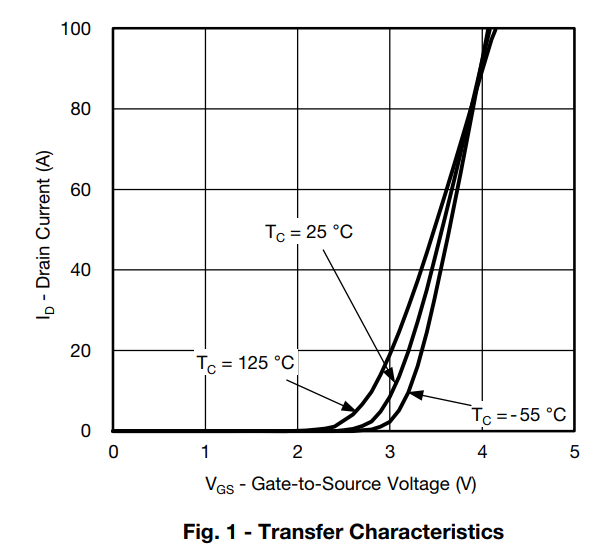
If we refer to the curve as shown above we realize that for 20 Amp drain current, 3.2 V gate-to-source voltage may not be adequate.
The combination would result in a VDS of 10 V typically with a dissipation of 200 watts.
Transfer curve data can be useful for MOSFETs operated in the linear range, however the curve data may have less significance for MOSFETs in switching applications.
Output Characteristics
The curve which reveals the actual data regarding the fully ON condition of a MOSFET is known as the output curve as shown below:
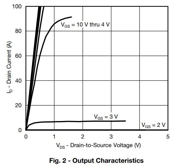
Here, for the various levels of VGS the forward drop of the MOSFET is measured as a function of current. Device engineers use this curve data to confirm the optimal level of gate voltage.
For each level of gate voltage that ensures a full switch ON of the MOSFET [RDS(on)], we get a range of voltage drops (VGS) across drain-to-source having strictly linear response with drain current. The range begins from zero and upwards.
For lower gate voltages (VGS), when the drain current is increased, we find the curve losing the linear response, moving through the "knee" and then going flat.
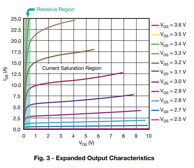
The above curve details provide us the complete output characteristics for a range of gate voltages from 2.5 V to 3.6 V.
MOSFET users may normally contemplate this as the linear function. However, in contrast device engineers may prefer to pay more attention towards the gray region of the graph which suggests the current saturation region for applied gate voltage.
It reveals the current data that has touched the saturation point or the saturation limit. At this point, if the VDS is increased will result in a marginal increase in the current, but a small increase in drain current may lead to a much larger VDS.
For increased gate voltage levels, which enable the MOSFET to turn ON fully, the green shaded area will show us the operating point for the process, indicated as resistive (or Ohmic) region.
Please note that the curves here show the typical values only, and does not include any minimum or maximum boundaries.
While operating at lower ambient temperatures, the device will require higher gate voltage to stay in the resistive region, which may go upward at the rate of 0.3 %/°C.
What is MOSFET RDS(on)
When device engineers have to encounter the output characteristics of the MOSFET, they will essentially want to learn about the RDS (on) of the device with reference to the specific operating conditions.
Generally, this can be a mix of VGS and IDS across the area where the curve has deviated from the straight line into the portion indicated by the gray shade.
Considering the example discussed above, a gate voltage of 3.1 V with an initial current of 10 Amps, the engineers will know that the RDS(on) will tend to be greater than the estimated value. Having said this, do we expect the MOSFET manufacturer to furnish an approximate data regarding this?
With both the quantities VDS and IDS readily obtainable in the curve it may become too enticing, and is often surrendered into, to divide the two quantities at the resultant RDS(on).
However, sadly we do not have an RDS(on) for the assessment here. It seems to be unavailable for the mentioned situations since for any section of the load line representing a resistance has to cross through the origin in a linear manner.
That said, it may be possible to simulate the load line in an aggregated form like a non-linear resistance.
At the minimum, this will guarantee that any understanding of practical working is sustained at the origin (0, 0).
Gate Charge Curve Characteristics
It is the gate charge curve data that actually gives us a real hint regarding the turn ON specs of the MOSFET as shown in the figure below:
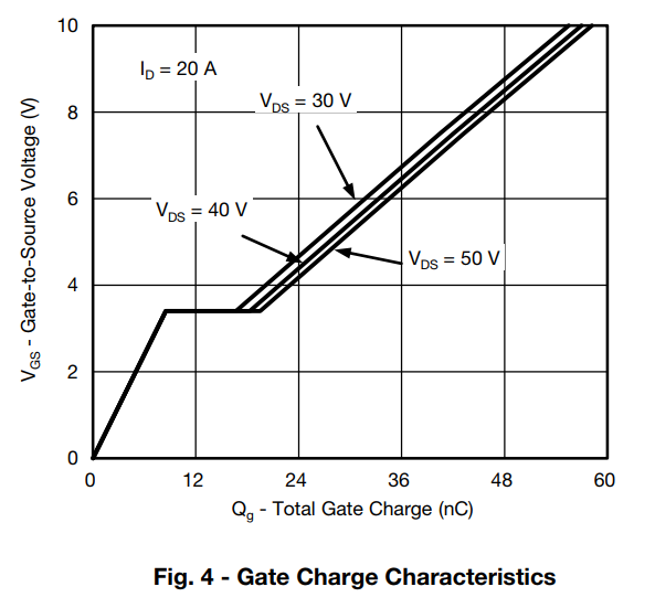
Although the above curve is a standard inclusion in all MOSFET datasheets, the underlying indications are seldom comprehended by the MOSFET user.
Moreover, the modern advancement in the MOSFET layouts, such as trench and shielded gates, call for a revised addressing of the data.
For example, the specification named "gate-charge" may appear slightly misleading by itself.
The linear and divided sections of the curve do not appear like voltage charging a capacitor, regardless of how much non-linear value it may exhibit.
To be precise, the gate charge curve signifies an associated data of two non parallel capacitors, having dissimilar magnitudes and carrying different voltage levels.
In theory, the functional capacitance as witnessed from MOSFET gate terminal is defined with the equation:
Ciss = Cgs + Cgd
where Ciss = gate capacitance, Cgs = gate source capacitance, Cgd = gate drain capacitance
Although it may appear rather simple to measure this unit and specify in the datasheets, it must be noted that the term Ciss is actually not a real capacitance.
It may be completely wrong to think that a MOSFET is turned ON merely through a voltage applied on the "the gate capacitance Ciss".
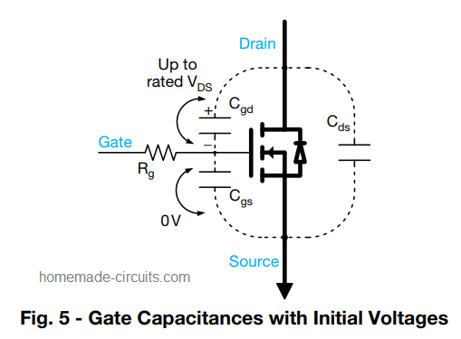
As indicated in the above figure, just before a MOFET turns ON, the gate capacitance has no charge, but the capacitance at gate-drain Cgd possesses a negative charge which needs to be eliminated.
Both these capacitance have a non-linear nature and their values largely vary as the applied voltages vary.
Hence, it is important to note that it is the stored charges of the MOSFET that determines its switching characteristics, and not the capacitance value for a specific voltage level.
Since the two capacitance elements constituting Ciss have different physical attributes, they tend to get charged with dissimilar voltage levels, requiring the turn ON process of the MOSFET also to go through two stages.
The precise sequence may be different for resistive and inductive applications, but typically most practical loads being highly inductive, the process could be simulated as depicted in the following figure:
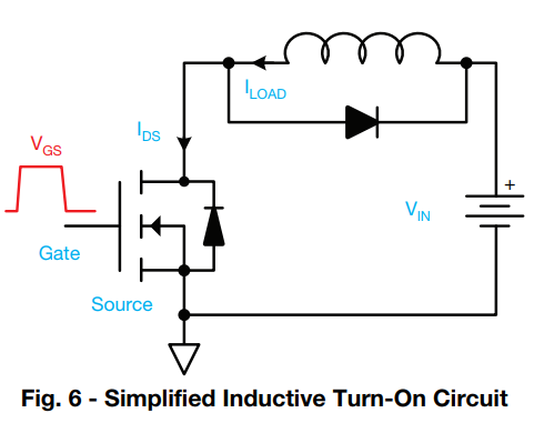
Gate Charge Timing Sequence
The gate charge timing sequences of the MOSFET can be studied from the diagram below:
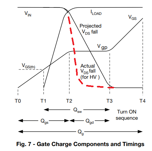
It may be understood with the following explanation:
- T0 - T1: Cgs charges from zero to VGS(th). VDS or IDS does not go through any changes.
- T1-T2, current starts rising in the MOSFET in response to the increasing gate voltage from VGS(th) upto the plateau voltage Vgp.
- Here, IDS increases and reaches to full load current from 0 V, although VDS remains unaffected and constant. The associated charge is formed through the integral of Cgs from 0 V to Vgp, and Qgs given in the datasheets.
- T2 - T3: Observe the flat region between T2 and T3, it's called the Miller plateau.
- Before the switch ON, Cgd charges and holds up to the supply voltage VIN, until IDS reaches the peak value I(load) at T2.
- The time between period T2 and T3, the negative charge (VIN - Vgp) gets converted into positive charge with respect to the plateau voltage Vgp.
- This can be also visualized as the falling of the drain voltage from VIN to around almost zero.
- The charge involved is equal to around the Cgd integral from 0 to Vin, which is shown as Qgd in datasheets.
- During T3 - T4, the gate voltage climbs from Vgp to VGS, and here we find hardly any change for VDS and IDS, but the effectual RDS(on) drops slightly as the gate voltage rises. At some voltage level above Vgp, provides the manufactures enough confidence to fix the upper limit on the effective RDS(on).
For Inductive Loads
The rise of current in MOSFET channel due to an inductive load needs to be completed before the voltage starts falling.
At the start of the plateau, the MOSFET is in the OFF state, in the presence of a high current and voltage across drain to source.
Between the time T2 and T3, a charge Qgd is applied to the gate of the MOSFET, wherein the MOSFET characteristic transforms from constant current to constant resistance mode at the end.
When the above transition happens, no noticeable change in the gate voltage Vgp takes place.
This is the reason it is never a wise idea to relate a MOSFET turn ON process with any particular level of gate voltage.
The same may be true for the switch OFF process, which demands the same two charges (discussed earlier) to be eliminated from the gate of the MOSFET in the opposite order.
MOSFET Switching Speed
While Qgs plus Qgd together ensures that the MOSFET will switch ON fully, it does not tell us about how quickly this will happen.
How fast the current or voltage will switch is decided by the rate through which the charge elements at the gate are applied or removed. This is also termed as the gate drive current.
Although a fast rise and fall rate ensures lower switching losses in MOSFETs, these may also give rise to system level complications related to increased peak voltages, oscillations, and electromagnetic interference, especially during the turn off instants of the inductive load.
The linearly falling voltage depicted in the above Fig.7 manages to take a constant value of Cgd, which may hardly happen to MOSFETs in practical applications.
To be precise, the gate-drain charge Cgd for a high voltage super junction MOSFET such as SiHF35N60E exhibits a significantly high linear response, as can be seen the following figure:
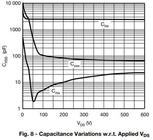
The variation range that exists in the value of Crss (reverse transfer) is more than 200:1 within the initial 100 V. Due to this the actual fall time of voltage against the gate charge curve appears more like the dashed line shown in red color in figure 7.
At higher voltages, the rise and fall times of the charges, along with their equivalent dV/dt values are more reliant on the value of Crss, instead of the integral of the whole curve indicated as Qgd.
When users want to compare MOSFET specs within different design environments, they should realize that MOSFET with half the Qgd value won't necessarily feature two times faster switching rate, or 50% less switching losses.
This is because, according to the Cgd curve and its magnitude at higher voltages, it may be quite possible for a MOSFET to have a low Qgd in datasheet, but without any increase in the switching speed.
Summarizing
In actual implementation, the turning ON of a MOSFET happens through a series of processes, and not with a predetermined parameter.
Circuit designers must stop imagining that VGS(th), or voltage levels could be used as the gate voltage for switching the MOSFET output from high to low RDS(on).
It may be futile to think about having an RDS(on) below or above a specific gate voltage level, since gate voltage level doesn't intrinsically decide the turn ON of a MOSFET. Rather it's the charges Qgs and Qgd introduced into the MOSFET that execute the job.
You may find the gate voltage rising above VGS(th) and Vgp during the charge/discharge process but these are not so important.
Likewise, how fast todays MOSFET may turn ON or OFF can be a complex function of Qgs or Qgd.
For evaluating MOSFET switching speeds, especially the advanced MOSFETs, the designer must go through a comprehensive study regarding the gate charge curve and the capacitance characteristic of the device.
Reference: https://www.vishay.com/

Comments
Hi Mr Swagatam;
At the mosfet source pin of the 72V battery charger circuit there are about 320V and I see about 90V AC at the drain pin. I think that means UC3845 is in good condition and primary side of the smps is OK.
If possible I need your comment.
Hi Suat,
It is will difficult to judge with those specifications. Is the IC and the MOSFET oscillating the primary winding of the transformer, we have to confirm this first?
hi dear sir, thanks for your article, i want to know how to choice the gate driver ic for a mosfet. I don’t know how to calculate Ig. Can I choice the ic which Io>Ig?
Ig=Qg/(td(on)+tr), is this right?
Hi Zhouzhou, honestly, I have never used any formula to calculate the gate driver, so I cannot suggest whether the formula is correct or not. I simply use the following design and it works very efficiently.
great man ,suppose if we want to ask you a question and we can not find the article related to it,how can we seek your help to solve for our need for the desired circuit,
right now i need a circuit and i not able to find an article about it on your wonderful site ,i want to convert a voltage 0 v to 12 v
to a variable resistance of 100 ohm to 3 k ohm ,could you please suggest a circuit related to the above mentioned circuit
Sedigh, your question involves the term “voltage” therefore it should have been posted under any “power supply” related article.
Sorry I have no idea how a voltage can be converted to resistance, may be you can clarify a little bit more.
hi dear sir i want to use a mosfet as a key for dim car’s light
and want to use mosfet instead of a relay and i need a
circuit to vary the light of the car lamp
can you please offer me a circuit for my need
i look forward to your reply and thank you in advance for your help
Sedign, I have updated the circuit at the bottom of the following post
https://www.homemade-circuits.com/replacing-conventional-automotive/