In this post I have explained how to make a simple, cheap yet extremely reliable smps based 220V/120V mains operated cell phone charger circuit.
Why TNYxxx Tiny Switch is Used
The TNY series of tiny switch ICs provide us with an option of making perhaps the smallest possible smps circuits with high reliability. The tiny switch series includes the following ICs: TNY267P, TNY263, TNY264, TNY265, TNY266, TNY267, TNY268, TNY280.
The above ICs have an integrated in-built mosfet switching control circuit, protection against over current and thermal overshoot, along with rugged voltage and current specifications.
The IC comes in a DIP8 package that's exactly how a 555 is enclosed. The maximum tolerable voltage limit of the TNY series ICs is a massive 700V, a margin that's way beyond our normal household AC specs. The operating frequency is at about 132kHz.
The IC is specifically designed and built for implementing compact and reliable 120/220V mains operated SMPS flyback converters.
Although the application of the proposed simplest SMPS design could be huge, it could be best used as a mains operated 5V cell phone charger circuit.
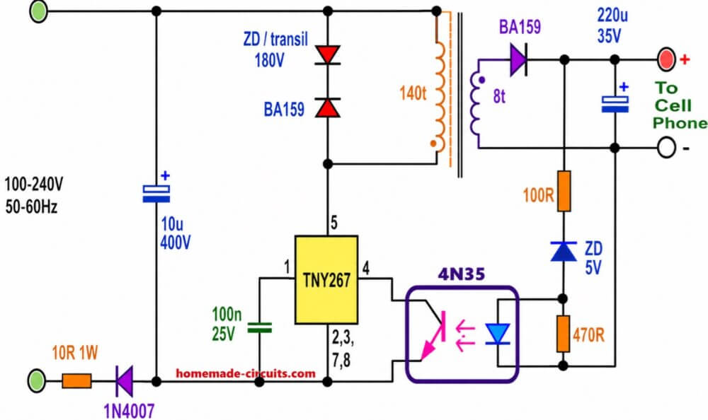
The proposed cell phone charger design using the IC TY 267 can be visualized in the below shown diagram.
Audio/Video Representation
How the SMPS Circuit Works
The circuit can be understood as follows:
The mains input which could be anywhere between 100 and 280V is half wave rectified and filtered through shown 1N4007 diode and 10uF/400V input rectifier stage.
The 10 ohm/1watt resistor is included to provide some sort of restriction against the surge current inrush during power switch ONs and also forms like a fuse in case of a catastrophic situation.
The switching voltage is acquired via the BA159 diode at pin5 of the IC.
The IC instantly locks into the specified 132kHz switching frequency when switched ON across the input winding of the switching ferrite transformer.
The 180V zener diode safeguards the IC from peak switching voltages.
The above switching generates the calculated stepped down low voltage across the output winding of the transformer.
The BA159 diode at the output rectifies the 132kz pulsed DC while the 220uF capacitor filters the high frequency ripples to produce a clean DC.
The optocoupler acts like a feedback link between the output and the IC in order to ensure that the output never exceeds a certain predetermined voltage level.
This feedback limit is decided by the adjoining 4.7V zener diode, which ensures that the output stays well within the 5 V range just suitable for charging any attached cell phone.
How to wind the ferrite transformer
The shown ferrite transformer along with the IC forms the heart of the circuit, however due to its simple configuration winding this transformer is much easier compared to other mains operated cell phone charger circuit topologies.
The input primary winding consists of around 140 turns of 36 SWG, while the output secondary winding is made up of 8 turns of 27SWG super enameled copper wire turns.
The core used can be a small E19 type ferrite core with bobbin having a central core area section measuring 4.5 by 4.5mm.
The primary is wound first. After winding it, it must be covered with a layer of insulation before winding the 8 number of secondary turns on top of the primary layer.
A copper or aluminum tape layer should be preferably included in between the primary and the secondary winding and a wire connected with this tape with the "cold" end of the primary winding (see the trafo in the figure), this provides guaranteed isolation between the winding as well as guards against interference issues.
Transformer Winding Calculations
We can use the following standard formula for calculating the transformer primary and secondary turns:
B = Vin * Dmax / (Np * Ae * f)
Assuming the core is EE19, then Ae can be taken as 30 mm2 and Bmax = 0.25 Tesla...
Substituting in the above equation gives:
0.25 = 310 * 0.45 / (Np * 30 * 10⁻⁶ * 132000)
Np = 140 turns
Secondary Turn formula is:
Vout = (Ns/Np) * Vreflected
Assuming reflected voltage as 80V, then
5 = (Ns/140) * 80
Ns = 8 turns


Questions & Answers
Sir
pleas discribe the diameter of the copper wire in terms of mm
joshua, you can try any online calculator chart for the conversions.
dear Sir,
How to increase the output voltage (say 12) and current (say 500mA)
dear token,
each turn for the secondary winding will roughly add 1V at the output, so you can put about 16 turns for the secondary and also make sure ZD is selected with the same value
the current can be increased by using bifilar winding for the secondary.
i have an question on the construction of the transformer.
a copper or alluminium tape must be connected to the primary winding?
then the sequence is:
1) winding the primary
2) isolation tape
3) copper tape connected to primary winding
4) isolation tape
5) the secondary winding
tell me please if this is correct.
thank you so much
regards
andrea
yes that's correct, connect the copper tape with the cold end of the primary, meaning with the line which connects with 180V zener anode.
Sir i have a ready-made mobile smps circuit.
its output is 5v with 500mA.
Can i increase its rating upto 1A and 12v by altering the secondary winding.?
Syed, yes it can be done, if there's a corresponding zener at the output that will also need to be modified accordingly.
hai swagatam,
I have doubt that does this circuit can be enhance to 5v 1.5 amps
hi arvind, yes it can be possibly done by using bifilar or trifilar winding over the transformer
sir can be use this circuit as constant current,if yes then please tell me the modification.
Naresh, the circuit will require some modification for implementing this, which can be slightly complex, it's better to add a LM317 current controller at the output for controlling current.
The first circuit from the following article can be tried:
https://www.homemade-circuits.com/2013/06/universal-high-watt-led-current-limiter.html
sir your soggetion is very good,because LM317 is a very accurate to control ccurrent,but it's maximum output is around 35 volts, please suggest me another regulator whose output is around 60 to 70 volts.
Again Thanks
OK, in that case you may include the circuit shown in the following link:
https://www.homemade-circuits.com/2011/12/make-hundred-watt-led-floodlight.html
T1/T2 may be any NPN rated to handle the desired voltage and current specs
Thank you for your quick response
Swagatam,
Firstly, Thank you for this great blog. I have really liked reading the posts since last couple of days. And it has given me knowledge and ideas to solve an SMPS design problem I have at hand for a project.
I am not an electronics expert and have managed to acquire some basic knowledge only over the last 10 days. This post i think i find most closest to the problem i have.
SMPS Design Requirement:
Input: 90 – 230 V AC
Output1: 5 V DC / 1.5 Amps (Max)
Output2: 12 V DC / 1 Amps (Max)
Output3: 5 V DC / 1 Amps (Max)
Out1 and Out2 are for 2 different microprocessors.
Out3 is for a switching and phase control of triacs for resistive and inductive loads both. This also needs a zero cross detector pulse coming from the SMPS to be used for phase control.
All outputs must be regulated and shall provide isolation to the loads.
Can this design be used for this requirement? say by modifying the transformer secondary windings as per the desired output voltages and current. May be with a few more components, for eg. each output will need error correction like the optocoupler and TNY267 in this design.
So, Is this possible using the same design? With off course minor modifications but keeping the basic idea same. I like this idea for its small size, I want the SMPS PCB to be small, say a credit card size or smaller.
Please advice.
Thanks
Thanks very much Kernel,
I think you should try the following design instead, as its much sophisticated and will suit your application need quite well:
https://www.homemade-circuits.com/2012/03/how-to-make-simple-12-v-1-amp-switch.html
the amp rating can be slightly increased by increasing the SWG of the secondary winding
sir can you please mention what will be the primary and secondary inductances for the transformer?
Sumit, the inductance values are not important, if you wind the transformer as per the given data it will surely work, just make sure the E cores are separated by a paper gap or by inserting the insulating tape
Sir, didn't fully understand the last part. should the two E cores facing each other need to be insulated from one another?
The joining surfaces of the E cores must not touch directly with each other rather must be separated by sandwiching a piece of paper between the surfaces or by inserting the insulation tape itself which would be used to fasten the E cores around.
Thanks. And one more question, can the TNY series ICs be used for a 12V SMPS? Actually on a datasheet I came across, I found that the TNY267PN has an output voltage of 5V. Please suggest whether the information furnished is correct if so then what can I do. Thanks.
TNY is an oscillator IC it has no relation with the output voltage of the SMPS….the output is determined by the transformer secondary winding and the feed back zener value
Kudos for a great informative article, in fact the blog deserves applause. Swagatam sir, I am designing a project to control LED Bulb running off 220v with microcontroller @3.3v. Since bulb is constrained on space, a compact circuit like yours is suitable. But how can I get 80v 150ma constant current for LED and 3.3v 500mA for mc from same circuit? Your kind help Wii be greatly appreciated.
Thanks so much hkarya, since each turn corresponds to around 1V, so around 80 to 100 turns at the secondary side of the trafo would roughly provide you the required 80V. The 3.3V can be achieved by winding a separate 5 turns somewhere inside the transformer (secondary) and the terminals secured with a 7805 IC and a few 1N4007 diodes in series for generating 3.3V.
the opto now should be used for the 80V outputs, with the existing 5V zener replaced with a 80V zener diode
I have a question that can I use tny266 or tny268 in place of tny267 and 4n35 in place of sfh6106 optocoupler.
Thanks.
yes, you can use those instead of the indicated ones in the diagram
I could not find how much current it can supply at 5 volt.
Thanks,Anurag Gupta
around 1 amp
I am not able to understand why a dotted line is shown from the transformer winding,basically i want to know if there are any other additional tappings from the transformer for feedback,etc.Also i want to know if the tranformer requires lamination sheets? I have seen some transformers in battery charger which dont have a core of laminations around it.
It's a blank winding sandwiched between the primary and secondary winding, one end is pressed between the two winding and remain unused while the other end is soldered with the cold end of the trafo as shown…
Do i have to buy separate lamination sheets for core or e19 ferrite core is available readymade?Actually i have never wound a transformer before.
ferrite cores are not made up of lamination, they are available readymade in the market as whole solid "E" shaped cores…so you can easily buy these from the market as per the required specification and size.
I have made the above circuit ,I have used 4 47v zener diode(=188v), the response is very random:
voltage across 400v cap=450v
across primary winding:870-880v(ac) i get voltage across primary sometimes ,sometimes not.this is bothering me, also it it is too high.
across pins 5(drain) & 8(source)-370-380v(dc).
once i got a voltage of 1.4-1.5v across the output cap without any voltage on the primary winding,i think. Its hard to say but i think the main problem is of switching of the tny267pn ic.
Any suggestions for troubleshooting?
Also i am using sfh6106-2 its ctr is 63% to 125% whereas sfh6106-1 has 40-80% and a 100nf cap ceramic(not electrolytic at pin1 of ic) and a 6v zener diode at output.
sorry troubleshooting will be difficult because I am don't know how you have built the transformer which is the most critical component in the design and requires experienced hands in order to create a perfect trafo, anyway you can try the following design also…this IC is much reliable than the TNY, and will give guaranteed results
https://www.homemade-circuits.com/2012/03/how-to-make-simple-12-v-1-amp-switch.html
I wound the transformer again nicely and tightly first primary,then tape then cardboard then connected 36swg wire to the primary zener end and wound a turn of it and then Al or Cu tape then tape then secondary then tape again .Also provided a paper and tape gap between the cores.Then I noticed that i had not connected 8 th pin drain of ic to the negative of 400v cap or 100nf 25v cap so i connected it to the nearest 400v cap and tested it again and there was a spark in front of my eyes blowing up the tny ic especially at the 5th pin the ic package was blown off there.I think i did everything right. I also want to know how to check if the optoisolator is working properly i did with a multimeter and i found it wrong.
did you connect the output diode to the "start" pin of the secondary?…see the black dots on the transformer it indicates the start of the winding…so it must be followed in that way.
you can go through the following datasheet for a detailed info regarding the circuit
http://www.mouser.com/ds/2/328/tny263_268-8433.pdf
by the way don't bother about the central screening winding, remove it…and wind only the primary and the secondary with just a few turns of insulating tape between them.
if the output stays controlled at the specified zener voltage value that will confirm the opto working
If you mean by start of the secondary that from where we start winding the transformer then no i did not connected it to the start of the secondary but do you think it can lead to blowing up of the ic which is protected by both optoisolator and zener diode of 180v.Also is there a way to check optoisolator ic off the circuit alone.I measured resistance across the diode ,it should have offered high resistance in one direction and low in other but it wasn't so i think the opto ic may be wrong too.
Also can i use a zener of less than 180v if yes how low?
you must do exactly as indicated in the circuit diagram, the diode should be connected to the start pin of the secondary…you can consult a professional transformer designer to confirm the transformer polarity.
the central screening winding can be eliminated it's not compulsory…and wind only the primary and the secondary with just a few turns of insulating tape between them.
If you don't want the 180V zener, you can replace it with the set of components as shown in the second diagram of the following datasheet
http://www.mouser.com/ds/2/328/tny263_268-8433.pdf
the TNY is not an optocoupler….it's an integrated circuit so you cannot check it the way you may check a normal 4 pin opto isolator.
…ignore the last sentience it's incorrect…I thought you were trying to the check the TNY….yes the optocoupler LED can be checked just as we check a normal LED for its polarity.
How do you check transformer polarity, can't i check it myself the polarity? I made a sine wave generator using wien bridge oscillator which generated 6v rms but when i connected it to the primary the voltage dropped to 0.2v then i measured the primary resistance which was 3ohm so (6v/3)2A current was required which could not be supplied by the battery ofcourse.
Also i cant connect it to a dc source as it is designed for 130khz even if i use a function generator it cant supply 2A i think.Please tell me if i am wrong somewhere.Isn't there a simple way to check polarity?Can u give any link or tips for transformer design i want to test the circuit shown in tny datasheet which shows 5v 2A output plus 12v 20ma output.Also,in the circuit how much ac voltage is expected to be at the primary?
And thanks a lot i have been bothering you for quite a bit now.
inductor polarity is determined by the start and finish pins of the winding. By marking the start and the finish pins you can confirm the connections with correct polarity.
first try to complete the above design successfully then you can move on with other difficult versions.
the best thing would be to use a bridge rectifier at the secondary this will ensure a fixed polarity across the output of the bridge regardless of the secondary winding connections.
Yeah i knew where i started and where i ended the winding and connected with correct polarity(if dot means the start of winding) and used the rcd snubber u mentioned with 1nf 1kv(i did not have 2.2nf) and thats why i used a 270k resistor in parallel instead of 200k and placed a 220 ohm in series with ba159 and used 4n35 optoisolator.
But the ic blew off again at the 5th pin drain of tny and i think now the main problem is the voltage spike generated by the leakage inductance of the trafo.
Now, i am going to use the clamp shown in at page 7. http://www.power.com/sites/default/files/PDFFiles/der228.pdf
Capacitor 2.2nf 1kv and tvs diode p6ke150a 150v 600w tvs diode as shown in the pdf .
I have only one tny ic left.. please tell if the above clamp would work fine or any other best alternative for the clamp to suppress voltage spikes at pin5.
I am also going to use varistor on ac input for additional safety.
Thanks
Also I forgot to mention that it was different from the last time,last time when i switched on the supply ,the spark was almost instantaneous but this time it was 2-3 seconds delayed and the voltage build up gradually from 1.5 to 3.6 v(i think i even saw it reach 4v in the multimeter but thats when the ic blew not too sure).1.5 v was there due to the diode and zener drop i think in the beginning.
Also suggest should i test the above circuit without load or with load on the output side? If with load please tell what type of load can resistance be used a load for testing purposes?
whether with load or without load, it should not matter, under any condition the circuit should work normally.
I think you should the try the second circuit that's explained in this article:
http://www.mouser.com/ds/2/328/tny263_268-8433.pdf
for the transformer, primary is 140 to 150 turns using 36swg and secondary around 10 turns
the IC is quite rugged and reliable, it will not blow unless something is significantly incorrect or mismatched in the assembly.
try the design shown in the following article:
http://www.datasheetarchive.com/dl/Datasheet-016/DSA00284887.pdf
In the design 1n4007gp has been shown in the clamp but i think ba159 should be used as u have shown in the above because switching is done at high frequency and ba159 is a fast switching diode whereas 1n4005gp is not.I realised another mistake of mine that i did not change the cold end connection so i will rectify it too.
yes you are correct!
Yipee,the design worked after so much effort thank you so much.
The output was between 3.6v to to 3.7 v should i wind more turns on secondary or do i need to consider other factors i mean do i have to change components like zener on the output too for 5v output or anything else or simply increasing the turns would do.
OK great, try increasing the value of the zener diode to 6V or 9V and see the response if still the voltage does not increase then you can add a few more turns to the secondary.
iI could not find how much current it can supply at 5volt output.
Thanks.
it should be around 1 amp
Hi Dear Swagatam, how can a charge complete indication be implemented with this circuit?
thanks and warm regards,
Prashant
Dear prashant, it can be achieved by adding another circuit at the output…such as this:
https://www.homemade-circuits.com/2011/12/how-to-make-simple-low-battery-voltage.html
so i dont have a second side of this circuit and osciloscope shows that ic doesnt even start oscilating what am i missing? part list: half wave rectifier diode 45uf filter cap pin 5 to tr and tr to +340 pin 5 diode to +340. first pin to ground via 0.1 uf and the rest to ground ? what can be wrong tr primary 100t secondary 10t for osciloscope ic blows like a match every time i conect it.
if the IC does not oscillate it will blow of, and with the shown connections the IC is bound to oscillate.
This circuit is thoroughly tested so there's no doubt about the design, it's good.
the primary should be 140 to 150 turns minimum.
you can try the design shown in fig14 of the following article….the trafo ratio can be the same as indicated above.
http://www.mouser.com/ds/2/328/tny263_268-8433.pdf
….you can also try the design that's shown in the following pdf:
http://www.datasheetarchive.com/dl/Datasheet-016/DSA00284887.pdf
is there any ready made transformer in the market? or i really have to build it
can i buy that transformer at the market?
can i buy that transformer in the market?because im a beginner and i think building it needs experience
sorry no, it might be difficult to find a ready made one in the market, you can take the help of a professional transformer designer and get it made to order.
Sir,
I have made a mobile charger using 7805 and it is working fine but i have some issues with this
1- heat skin become too much hot .( when using in car)
2- the charging speed is too much low.
Can you suggest me any circuit based charger which convert 12v to 5 v 2a .
Syed,
the heatsink will become hot, you can try increasing the size of the heatsink….if the IC stays cooler the charging will be proportionately faster….so you can try using a larger heatsing for the IC, and make sure to apply heatsink paste or heatsink compound between the heatsink and the IC.
Ok Sir but is there any circuit based charger to charge mobile from 12v.
search for "buck converter circuit", you can try this concept for charging a cell phone without heat.
hi sir
need transformer for 5.6v 1A smart-phone mobile charger &
transformer expert asking about the inductance
Hi Prasad, where is the schematic? which schematic are you referring to?
Hello sir
I m Rafiq Sherasia from Gujarat,
I m belongs to a small village where 1000 population…
In my village a big problem is getting very slow mobile signal…I am also electronic engineer.. And a shop of repairing AC/DC Drive in my nearest city…so my villagers told me that how to getting better mobile signal… I have many searching of this but not getting good answer…I told u that please help me to find out circuit for signal booster..wat to do for that…tell me any guidance… Me n my villagers are so thanx fully to u…
U can mail me
er.rafiq1989@gmail.com
9979113317
Hi Rafiq,
I don't think that would be feasible at our level, or at any level, if that would be possible you would have already seen such gadgets available in the market, but there's none so far.
Dear swagatam sir, please provide a circuit of mobile charger 5v 1 amp with BOM cost around Rs 15.
Dear Pradeep, that's impossible, you want a real mobile charger or a picture of it:)
Dear swagatam sir, I have build this smps. But i use 150V zd/transil(Part No: P6KE150A) instead of 180V since i couldn't find 180V one. And optocuplar is SFH610A-3. Others are exactly same as your one. But it's not work. Is there any way to diagnose transformer is oscillating and feedback is coming?
Dear Hasitha, It would be difficult for me to diagnose your circuit because there's hardly anything in the design that might go wrong.
I would suggest you to refer the datasheet of the IC there are a few good elaborate designs of the same in the datasheet with a few more components which might ensure a better chance of success.
Thanks sir, Now its work. It had a connection issue. Now the problem is as follows. I attached LED to the output. Its slowly blinking. Its light up and slowly go off and on again. Continuously this happen and no steady output. What would u think this issue?
It may be an indication that there's some kind of short circuit or overload in the secondary section, therefore the circuit is going in burst mode, that is the opto is trying to reset the primary repeatedly to correct the issue…not sure where the problem is, it could be in the secondary winding or the around the optocopler stage
I think i had transformer winding issue. I wound both primary and secondary same direction in clock wise. Do i need to wind secondary from other direction? like primary left to right then secondary right to left both clock wise. Can u please explain this.
the black "dots" near the winding indicate the start points of the relevant winding…you must follow these to get the correct results.
the primary and the sec winding ends are normally terminated across the two sides of the trafo. for easier identification and polarity check.
you can take the help of a professional winder for this.
Thanks again. very nice of you to return with this schematic diagram.
Do you think it is possible to buy the transformer ready to use?
You are welcome!
smps transformers are normally never available ready made in the market, you'll have to get it made from a professional winder.
AM
Dear swagatam sir, I want to build a smps 12v, 2amp for led driver can i use tny278 is for this pleas sir tell me about..
Dear Rahul, 2amp may not be possible from a TNY IC, you will have to go for a powerful mosfet based design.
Thank you very much for this informative article on a difficult topic ! Would you be able to comment on where to get the E transformer used in this design?
-Shashank
You can get them from any electronic retailer dealing with ferrite cores. you can also inquire online for the same.
Thanks … I reside in Pune and would appreciate leads on electronics retailers here or in Mumbai.
-Shashank
In Pune you can inquire in Budhwar-peth, and in Mumbai in Lamington Road
Sir, i need to charge a 2200 mAh mobile Battery will this circuit be enough. If not what are the changes to be done in this circuit. How to determine the output current for a specified mAh.
Nix, you can, but the charging will be a bit slower.
the ideal charging current should be 1.5 amps for your batt, and this circuit is specified at 1 amp max
I assembled the circuit.I made 16 turns as secondary winding and used pc 817 optocopler instead of sfh 6106, and a 12 v zenner in output feedback circuitry. But the result is blinking the led which I used in output as monitor led.When I shorted 12 v zenner with a jumper then it became steady but 3 volts observed in output with a DMM.Also 12 KHz was obtained with a frequency meter between transformer's secondary terminals .please help.
remove the 220uF and check again…if it improves then try adding another rectifier diode between the 100R and 220uF connections
I updated my hardware according to your advice. The led stop blinking, DMM shows 12 volts in out put but voltage dropped as soon as I connect a load (12v relay)into out put. Also frequency meter
shows around 14 KHz in transformer's secondary terminals.Sir do you think The ic does not oscillate at 132 KHz and as a result of that current capasity is so weak? Is it possible for the ic to be defective from the mamufacturar?
the primary winding is crucial and it determines the frequency as well as the correct functioning of the IC and the whole SMPS.
I would recommend you to visit the datasheet of the IC where you will be able to find a comprehensive information regarding the circuit and other specs related to the IC functioning
Sir. I went through data sheet and rewind transformer repeatedly but no result. At an instant, I connected the transformer wrongly(primary to secondary and secondary to primary)Then to my surprise,I found The ic didn't blown and result is same.So I suspect the device.
can we use the circuit to supply a microcontroller
yes you can
we can change tny by NCP1014 ?
Hello, instead of building the above design you can simply use the circuit from your spare mobile charger and use it for powering the MCU, but make sure to use a 7805 IC in between for regulation..
contrarily if you intend to build the circuit, do it only if you are well versed regarding switching circuits
the above circuit is extremely efficient, I am not very sure whether a bigger core would work or not, but you can try it with a fuse in series, in case if anything goes wrong.
yes any similar 4 pin opto coupler can be used