In this post we study the datasheet, pinout, and technical specifications of the IC LMC555 which is a CMOS version of the standard IC 555. The IC is equipped with many outstanding features, the most amazing being its minimum supply range which is down to 1.5V. Meaning now you have an IC 555 which can work even with a 1.5 V AAA cell, with guaranteed stable output.
CMOS stands for complementary metal-oxide-semiconductor, is a technology used for manufacturing improved semiconductor devices that enable them to work in a digital mode. Meaning, the devices respond only to well defined inputs and reject all spurious or undefined input signals.
Main Features
- Designed to Generate Record Fastest Astable Frequency at 3 MHz
- Comes with Smallest 8-Bump DSBGA Package (1.43mm × 1.41mm)
- Smallest Power Dissipation of around 1 mW at 5 V Supply
- Works with Voltages as low as 1.5 V Supply
- Being a CMOS Version Output can be interfaced Directly with TTL and CMOS Logic at 5 V Supply
- Tested with current from −10 mA, upto 50 mA Levels
- The IC shows minimum Supply Current Spikes while the Output is in the Transition phases
- Requires extremely minimal current for Trigger, Reset and Threshold actions.
- Great stability even with wide fluctuating ambient temperatures.
- Direct Pin-to-Pin Compatible With the normal IC 555 Series of Timers
Introduction
We all are very familiar with the industry standard IC 555 series, the proposed LMC555 IC is an advanced CMOS variant of this standard IC 555. The CMOS version is available in many packages apart from the standard package such as (SOIC, VSSSOP, and PDIP), and also in chip-sized "8-bump" incorporating Texas Instruments DSBGA package technology.
The main advantage of this CMOS LMC555 version is its ability to deliver the exact same features of the standard IC 555 such as precise time delays and frequencies, but with highly reduced power dissipation, and current spikes during pulse transitions.
While configured as a one-shot mode or monostabe mode, LMC555 generates accurate time intervals which is effectively controlled through a single external resistor and a capacior.
When it is operated in the astable mode. the output frequency, PWM and the duty cycle are ideally executed through a couple of resistors and a single capacitor.
Texas Instruments state-of-the-art LMCMOS process in the IC not only enables it to work with extremely low dissipation, it drastically extends the minimum supply range of the chip. It allows the use of a supply as low as 1.5 V yet provide a guaranteed operation for the IC, in its various modes.
Pinout Details
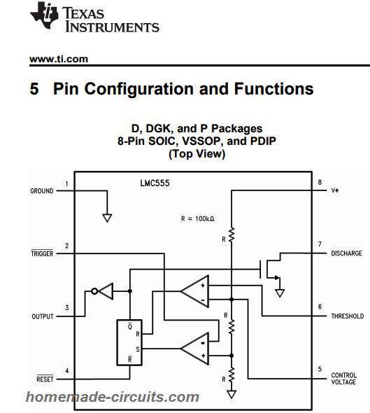
- Pin#1: Ground reference voltage
- Pin#2: Intended for changeover of the flip-flop through set to reset. The output of the IC is determined by the amplitude of the external trigger pulse placed on this pin
- Pin#3: Output
- Pin#4: You can apply a ground or negative voltage on this pin in order disable or reset the timer function. If not used for the resetting actions, make sure to connect the pin to VCC to enable proper triggering
- Pin#5: Control voltage pin is configured to control the threshold and trigger levels. It sets up the output waveform pulse. You can apply an external modulating signal on this pin to modify the output PWMs
- Pin#6: Analyzes the voltage applied to the pinout having a reference voltage of 2/3 Vcc. The voltage amplitude placed on this terminal influences the set condition of the flip-flop.
- Pin#7: Open collector output that discharges a timing capacitor across time intervals (in phase with output). It alternately switches the output from high to low when voltage extends to 2/3 of the supply voltage
- Pin#8: Supply voltage with respect to GND
Absolute Maximum Ratings
- Supply Voltage not to exceed above +15V
- Current output is maximum 100mA. Do not overload above this limit.
- Maximum soldering temperature nt to exceed above 150 degrees Celsius.
Detailed Description
Low-Power Dissipation
The LMC555 offers the same capability of generating accurate time delays and frequencies as the standard IC 555 but with much lower power dissipation. A power dissipation of less than 0.2 mW can be achieved with a 1.5 V operating supply voltage and less than 1 mW with a 5 V operating supply voltage. The use of TI’s LMCMOS process allows this low supply current and voltage capability. Reduced supply current spikes during output transitions and extremely low reset, trigger and threshold currents also provide low power dissipation advantages with the LMC555.
Device Functional Modes
Monostable Mode:
In this configuration, the IC works like a one-shot timer.
Initialy the internal circuitry keeps the external timing capacitor discharged. As soon as the negative trigger lower than 1/3rd VS is applied on the trigger input pin, sets up the internal flip flop causing a short circuit to be enforced across the external capacitor, which in turn causes the output pin to go high.
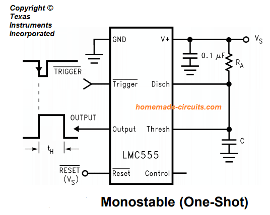
Subsequently, with no trigger signal, the voltage across the capacitor begins increasing exponentially for a time interval tH = 1.1 RAC equivalent to the time for which the output is held high, after which the voltage across the capacitor reaches 2/3rd VS. The internal comparator responds to this change and resets the flip flop, which quickly discharges the external capacitor reverting the output at its initial low state.
Astable Operation
In the astable mode as shown in the following figure (Threshold and trigger pins shorted), the circuit goes into a self-triggering mode, in the form of a free running multivibrator.
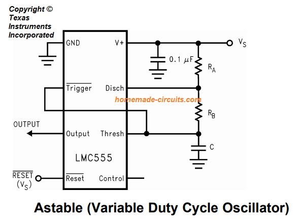
The resistor combination RA + RB , and RB alone alternately charges and discharges the timing capacitor respectively, generating a chain of continuous output rectangular waves, with a specific duty cycle.
Since the mentioned resistors control charging and discharging rate of the capacitor, implies that these resistors directly become responsible for determining the duty cycle of the output pulses, and their values can be altered appropriately for achieving the desired duty cycle.
Just like in the monostable triggered mode, here too the capacitor undergoes a charging and discharging process through the levels of 1/3 Vs and 2/3 Vs.
Application Circuits Using CMOS Version IC LMC555
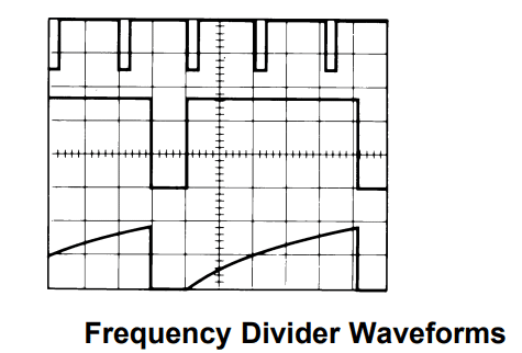
Frequency Divider
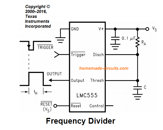
The monostable one shot configuration explained above can be implemented as a frequency divider by suitably changing the length of the timing frequency. The following figure shows the waveforms for a divide by three configuration.
Pulse Width Modulator
The IC LMC555 can be effectively used as a Pulse Width Modulator circuit or a PWM generator circuit by suitably modifying a monostable configuration as shown below.
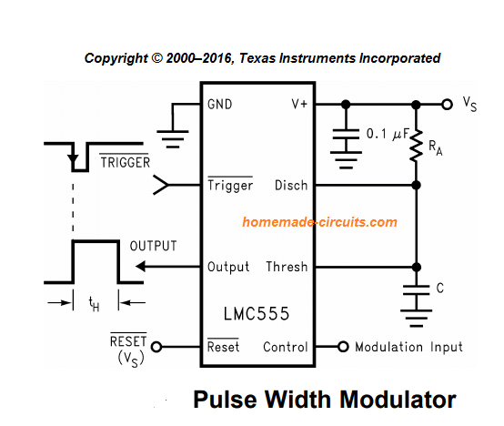
Here we can see that in the monostable mode if the trigger pin#2 is continuously triggered through an external square wave pulses, the output PWM from the IC can be modulated through a calculated signal applied at the control pin#5 of the IC.
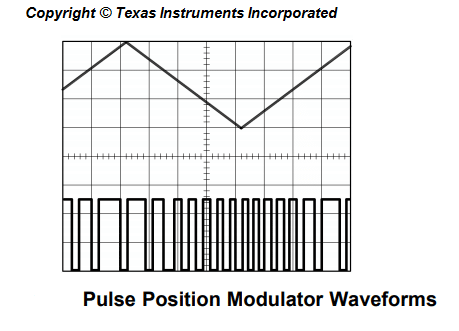
Pulse Position Modulator
In this configuration we are able to change the position or the density of the output pulses through modulating signal yet again applied on pin#5, which is the control pin of the IC.
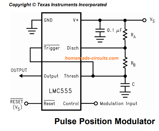
The IC is set in its astable mode, and a modulating signal s connected at the control pin of the IC, which causes the threshold voltage to vary with the signal and therefore the time delay of the PWM also vary proportionately. The waveform image clarifies the situation below.
50% Duty Cycle Oscillator
If you are looking for CMOS, TTL compatible 50% Duty Cycle Oscillator circuit, then this configuration can help to achieve the same with utmost efficiency. The following figure shows the bare minimum required for getting the specified results.
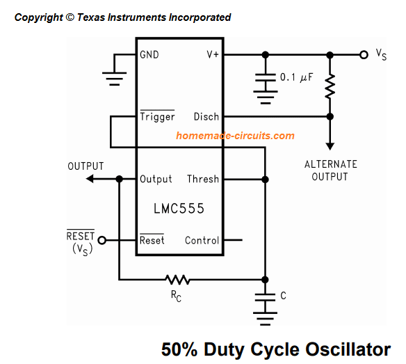
The formula for calculating the frequency is:
f = 1/(1.4 RcC)
Conclusion
- LMC555 is pin on pin compatible CMOS version of our standard IC 555
- The main advantage of this CMOS version is primarily extremely low power dissipation, and the minimum operational voltage range which is as low as 1.5 V.
- When operated with a 5V (CV), the output becomes perfectly compatible with TTL circuits, and 74 LS based designs.
- The standby current draw of this CMOS LMC555 is in uA, which is negligible compared to the normal IC 555 consumption which may be in mA.


Questions & Answers
I’m using a ic555 and it’s signal feeds a CD4050B which I can chain several gates to get a delay and I have a nice 4 volt pulse out put, but when I connect it to a 74HC7014 I lose the pulse. The cmos is voltage compatible at 5vcc with the ttl but I do not know how to make it current compatible. The ttl just says Icc 50ma max?
That shouldn’t happen since the CMOS or TTL inputs are extremely high impedance, so voltage can never drop at the inputs. Do you have a pull down resistor connected between the gate input and ground of the IC? If yes increase its value to 1M or more and check the response
Nice. Now I know the difference between the normal and CMOS 555