The popular LM317 voltage regulator IC is designed to deliver not more than 1.5 amps, however by adding an outboard current boost transistor to the circuit it becomes possible to upgrade the regulator circuit to handle much higher currents, and upto any desired levels.
You might have already come across the 78XX fixed voltage regulator circuit which are upgraded to handle higher currents by adding an outboard power transistor to it, the IC LM317 is no exception and the same can be applied for this versatile variable voltage regulator circuit in order to upgrade its specs for handling massive amounts of current.
The Standard LM317 Circuit
The following image shows standard IC LM317 variable voltage regulator circuit, using a bare minimum of components in the form of a single fixed resistor, and a 10K pot.
This set up is supposed to offer a variable range of zero to 24V with an input supply of 30V.
However if we consider the current range, it's not more than 1.5 amps regardless of the input supply current, since the chip is internally equipped to allow only up to 1.5 amps and inhibit anything that may be demanding above this limit.
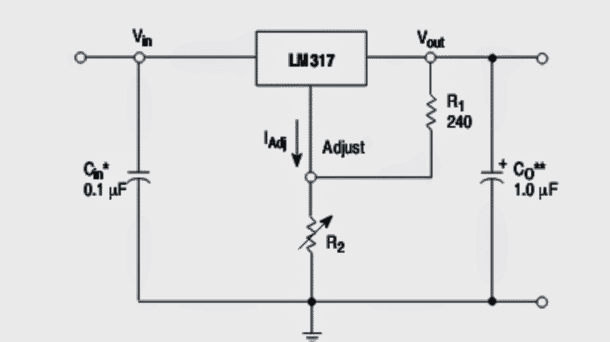
The above shown design which is limited with a 1.5 amp max current can be upgraded with an outboard PNP transistor in order to boost the current on par with the input supply current, meaning once this upgrade is implemented the above circuit will retain its variable voltage regulation feature yet will be able to offer the full supply input current to the load, bypassing the IC's internal current limiting feature.
Calculating the Output Voltage
For calculating the output voltage of a LM317 power supply circuit the following formula could be used
VO = VREF (1 + R2 / R1) + (IADJ × R2)
where is = VREF = 1.25
Current ADJ can be actually ignored since it is usually around 50 µA and therefore too negligible.
Adding an Outboard Mosfet Booster
This current boost upgrade can be implemented by adding an outboard PNP transistor which may be in the form of a power BJT or a P-channel mosfet, as shown below, here we use a mosfet keeping things compact and allow a huge current upgrade in the specs.
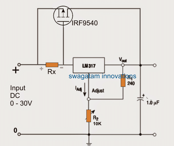
In the above design, Rx becomes responsible for providing the gate trigger for the mosfet so that it's able to conduct in tandem with the LM317 IC and reinforce the device with the extra amount of current as specified by the input supply.
Initially when power input is fed to the circuit, the connected load which could be rated at much higher than 1.5 amps tries to acquire this current through the LM317 IC, and in the process a proportionate amount of negative voltage is developed across RX, causing the mosfet to respond and switch ON.
As soon as the mosfet is triggered the entire input supply tends to flow across the load with the surplus current, but since the voltage also begins to increase beyond the LM317 pot setting, causes the LM317 to get reverse biased.
This action for the moment switches OFF the LM317 which in turn shuts off the voltage across Rx and the gate supply for the mosfet.
Therefore the mosfet too tends to switch OFF for the instant until the cycle perpetuates yet again allowing the process to sustain infinitely with the intended voltage regulation and high current specs.
Calculating MOSFET Gate Resistor
Rx may be calculated as given under:
Rx = 10/1A,
where 10 is the optimal mosfet triggering voltage, and 1 amp is the optimal current through the IC before Rx develops this voltage.
Therefore Rx could be a 10 ohm resistor, with a wattage rating of 10 x 1 = 10 watt
If a power BJT is used, the figure 10 can be replaced with 0.7V
Although the above current boost application using the mosfet looks interesting, it has a serious drawback, as the feature completely strips off the IC from its current limiting feature, which can cause the mosfet to blow-of or get burnt in case the output is short circuited.
To counter this over-current or short-circuit vulnerability, another resistor in the form of Ry may be introduced with the source terminal of the mosfet as indicated in the following diagram.
The resistor Ry is supposed to develop a counter voltage across itself whenever the output current is exceeded above a given maximum limit such that the counter voltage at the source of the mosfet inhibits the gate triggering voltage of the mosfet forcing a complete shut off for the mosfet, and thus preventing the mosfet from getting burnt.
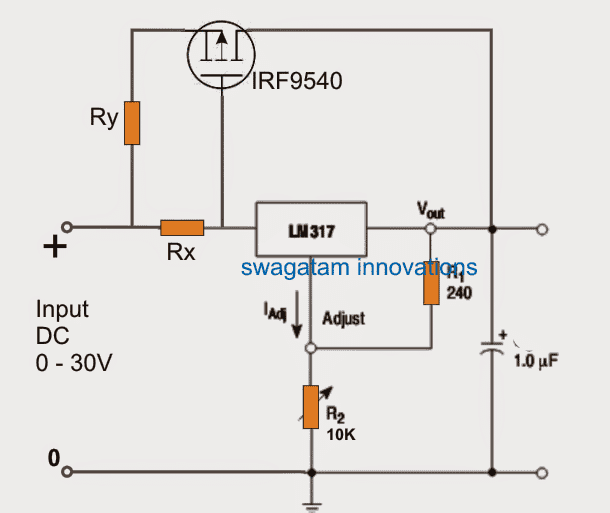
This modification looks pretty simple, however calculating Ry could be little confusing and I do not wish to investigate it deeper since I have a more decent and a reliable idea which can be also expected to execute a complete current control for the discussed LM317 outboard boost transistor application circuit.
Using a BJT for Current Control
The design for making the above design equipped with a boost current and also a short circuit and overload protection can be seen below:
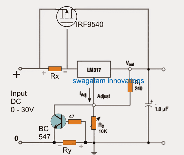
An couple of resistors, and a BC547 BJT is all that may be required for inserting the desired short circuit protection to the modified current boost circuit for the LM317 IC.
Now calculating Ry becomes extremely easy, and may be evaluated with the following formula:
Ry = 0.7/current limit.
Here, 0.7 is the triggering voltage of the BC547 and the "current limit" is the maximum valid current that may specified for a safe operation of the mosfet, let's say this limit is specified to be 10amps, then Ry can be calculated as:
Ry = 0.7/10 = 0.07 ohms.
watts = 0.7 x 10 = 7 watts.
So now whenever the current tends to cross the above limit, the BC547 conducts, grounding the ADJ pin of the IC and shutting off the Vout for the LM317
Using BJTs for the Current Boost
If you are not too keen on using mosfet, in that case you could probably apply BJTs for the required current boosting as shown in the following diagram:
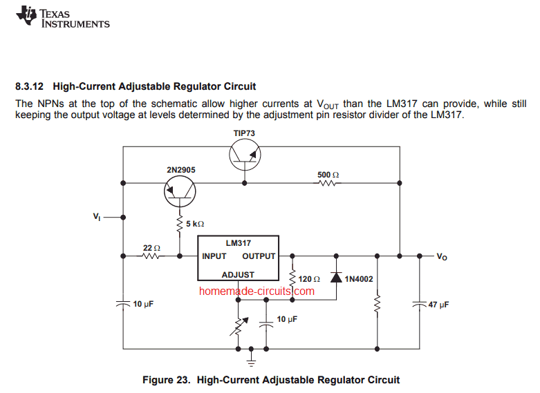
Courtesy: Texas Instruments
Adjustable Voltage/Current LM317 High Current Regulator
The following circuit shows a highly regulated LM317 based high current power supply, which will provide an output current of over 5 amps, and a variable voltage from 1.2 V to 30 V.
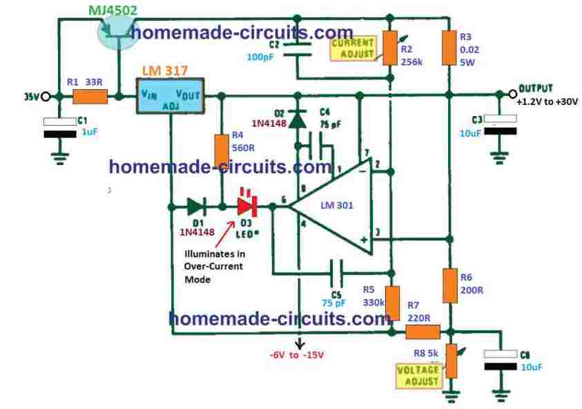
In the figure above we can see that the voltage regulation is implemented in the standard LM317 configuration through R6 pot which is connected with the ADJ pin of the LM317.
However, the op amp configuration is specifically included to feature the useful a full scale high current adjustment ranging from the minimum to the maximum 5 Amp control.
The 5 amp high current boost available from this design can be further increased to 10 amps by suitably upgrading the MJ4502 PNP outboard transistor.
The inverting input pin#2 of the op amp is used as reference input which is set by the pot R2.
The other non-inverting input is used as the current sensor. The voltage developed across R6 through the current limiter resistor R3 is compared with the R2 reference which allows the output of the op amp to become low as soon the maximum set current is exceeded.
The low output from the op amp grounds the ADJ pin of the LM317 shutting it off and also the output supply, which in turn quickly reduces the output current and restores the LM317 working.
The continuous ON/OFF operation ensures that the current is never allowed to reach above the set threshold adjusted by R2.
The maximum current level can be also modified by tweaking the value of the current limit resistor R3.
Another High Current LM317 circuit with Adjustable Current Circuit
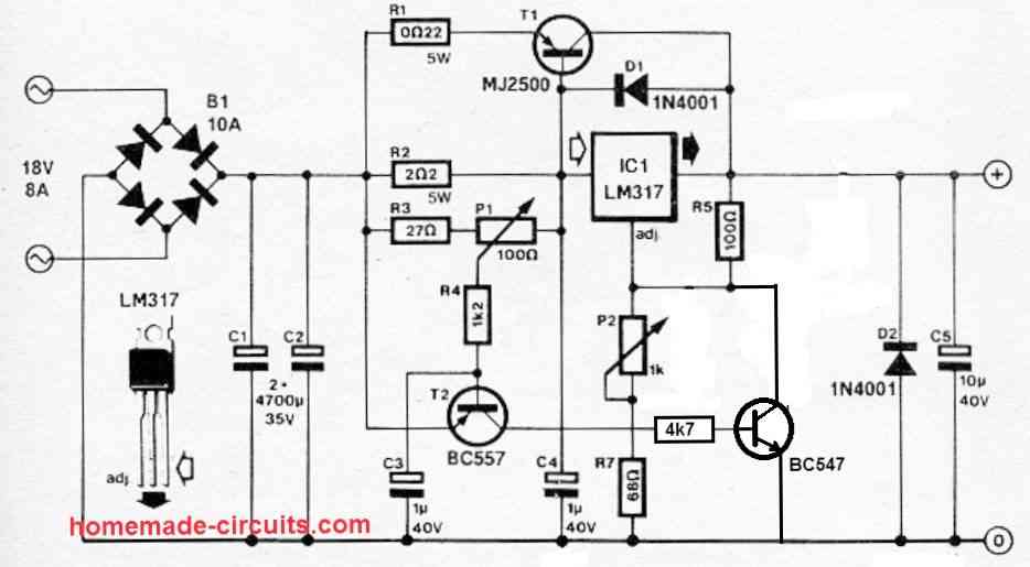
The following design also depicts an LM317 device configured with an external outboard transistor for achieving an enhanced high current output.
However, this circuit includes an improved current control feature, which is fully adjustable through a preset.
The idea is actually simple. Resistor R2 is rigged as the current sensor resistor.
When the output current exceeds the desired maximum limit, a proportionately increased potential is developed across the resistor R2.
This current is applied to the base T2, depending on the setting of the preset P1.
When this happens, T2 conducts and supplies the required base bias to the attached BC547 transistor.
The BC547 now begins conducting thereby grounding the ADJ pin of the LM317.
This causes the LM317 to shut down, and prevent the output current from exceeding any further.
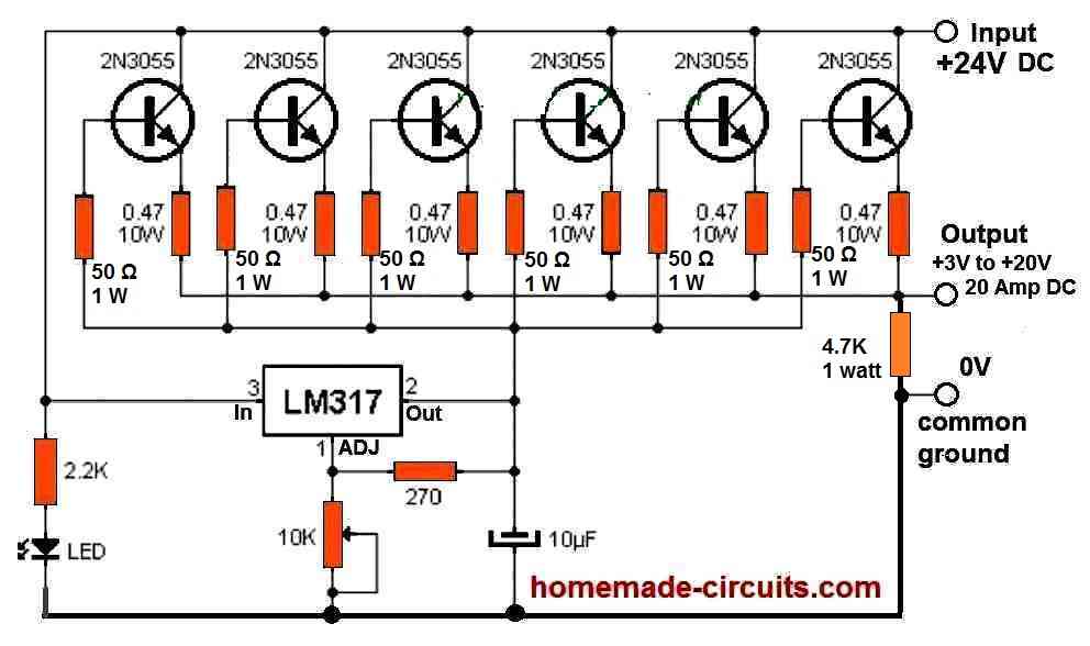
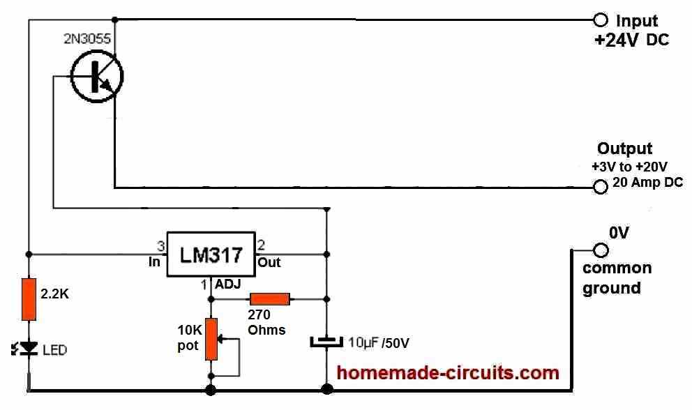
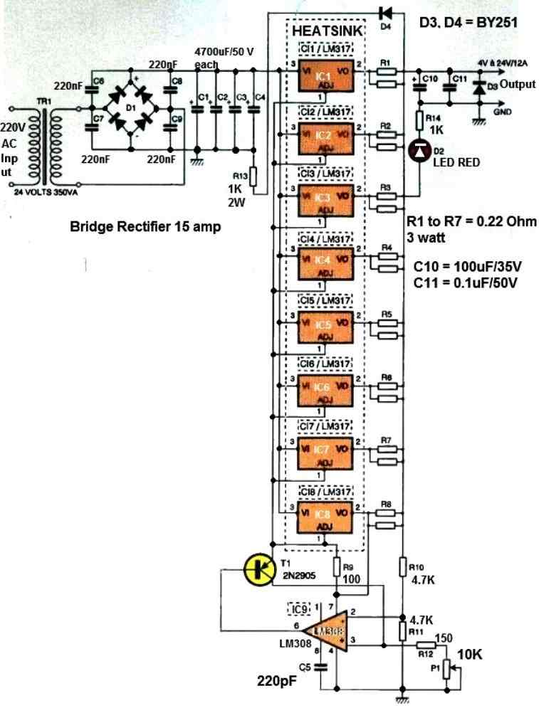
Using 6nos of 2N3055 to generate 20 amp current Output
Another very simple high current LM317 variable power supply can be built by connecting a few power transistors like 2N3055 in emitter follower configuration with the output of a standard LM317 power supply circuit as shown below.
The following design was contributed to this site by one of the avid readers of this blog, Mr. Moe through email.
Here's the details of the email as given below:
I have studied all your LM317 based power supply projects and have I have learned a lot from your wonderful posts. However; I assembled this very simple circuit below and it works very well. I would be very glad and thankful if you would please take a look at it to see if it is a perfect circuit or needs some modifications.
Using a Single 2N3055 with LM317 to Generate 5 amp output Current
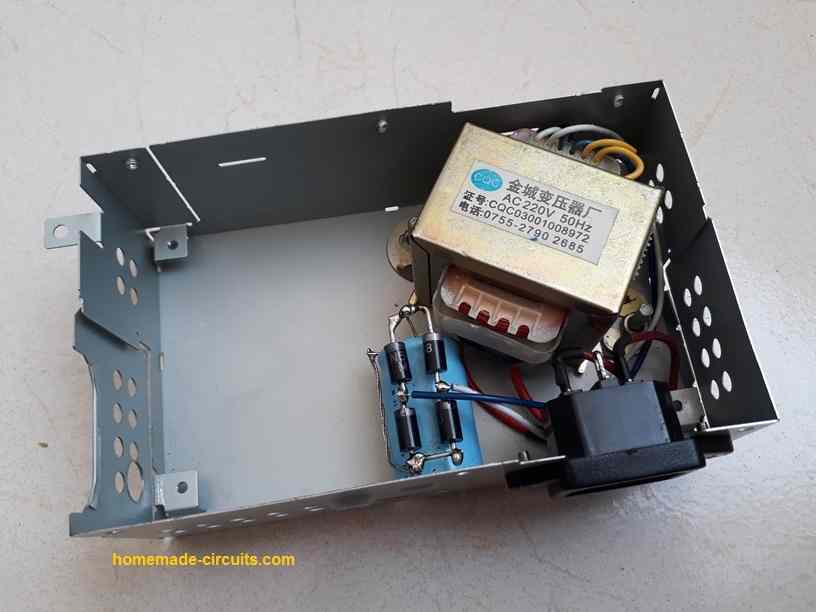
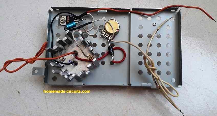
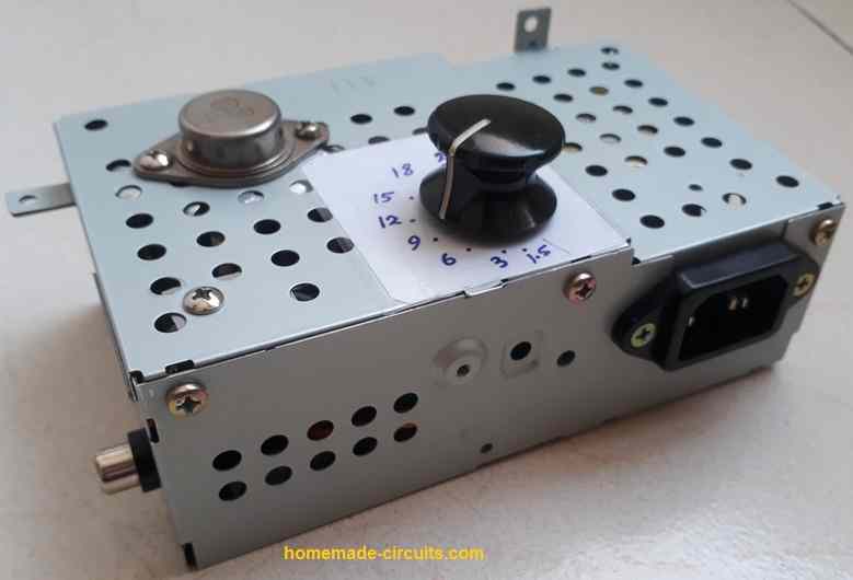
The above high current LM317 power supply using a single 2N3055 transistor was successfully built and tested by Mr. Ersa, who is a avid reader of this blog.
The following video test proof along with beautiful prototype images were contributed by Mr. Ersa:


Questions & Answers
Thanks for this. Note thought that near the begging you write "Rx = 10/1mA" but your description says 1A, not 1mA.
OK thanks, that looks like a typo, I'll correct it soon…
Hi Swagatam
Many thanks for this circuit. This circuit will be very useful for every electronic technicians, especially for beginers.
Hi Anil, It's my pleasure and thank you for suggesting me to post this important circuit concept.
Hi Swagatham
An LED or a Piezo buzer with internel ocilator can be added to indicate the short circuit condition. Where can I connect it in the last diagram.
Can I use an N-channel mosfet instead of P-channel after some modifications in the circuit….? If yes, how.
Hi Anil, using an NPN transistor will make the design very complex, so PNP is the only easier option…connecting a buzzer will be difficult because there's no appropriate space for it in the above design, however you can use a red LED in series with the BC547 collector for a short circuit indication.
resistor for the led on the collector of bc547 can alter the design? what is the voltage on the collector of 547 transistor and how can I calculate the resistor for the led?
connecting it in series with the emitter will be a better idea and a resistor can be avoided.
but in that case make sure the Ry formula is modified in the following way:
Ry = 0.6 + LED fwd Voltage / current limit value
Is this circuit tested and confirmed
yes…
sir what is the maximum current which can flow through this circuit.
It'll be as per your desired specs and requirement…
The last circuit design link seems to be broken, so I cannot see the circuit please upload a new one..And I think heatsink would be required to LM317 as well.
It is perfectly opening and visible to me here, just click on the diagram to enlarge it.
could you use a poly fuse for short circuit protection
it's not required
Hi sir, can i used a LM2940CT 12 Volt 1 Amp Low Dropout Regulator instead of LM317? thanks sir
Hi Em, yes it will do!
Hi Swa,
how are you ?
If i want to put an LED as short circuit indicator in series with the BC 547 collector, do we need to put a resistor in series to the LED? If so, how big is the value of the resistor?
Thanks
Kanta
Hi Kanta,
No it won't be required according to me.
Hi sir,
i just want to ask ,
if what is the possible connection.
to achieve 13.4V with 800mA current limit,
thanks
Hi Em,
It is possible, but the following design will be more suitable:
https://www.homemade-circuits.com/2012/02/how-to-make-current-controlled-12-volt.html
sir i am feeding the input pin of lm317 with 48V dc.. i need an output voltage of fixed 12V and 10A.. what modification i have to do ?
Moreover i dont have 0.07 ohm resistors with me.. the only resistors i am having are 3 no.s of 0.1 ohm 10 W resistors.. so please suggest a suitable circuit
RT, You can try the last circuit and calculate Ry as per the formula.
you can use many 0.1 in parallel which may yield 0.07 value approximately.
No other modification would be required according to me.
Hi, sorry I could not quite get your point, can you elaborate differently?
No the shown configuration in the last diagram is correct…the actual ground is supposed to be connected to Ry and the emitter of BC547 because the return path of the current must pass through Ry before reaching the transformer ground.
Hi Swag,
I used this circuit, because i tried to reach 5Amps max. Ry=0.14 Ohm.
But whenever i short circuit the output, the current goes 8-10Amps and the cut-off is not working.
I did a modification, connecting the Pot (10K) between collector and emitter on BC547 but still the same result. As i observed, whenever i do short circuit i don't have 0.7V on the base of BC547, but 0.55V. And on the collector voltage varies 1.6-2.5 depending of the position of the potentiometer.
Hi Nikola, you can try the second circuit and dimension Ry with some trial and error until the current is restricted at 6amps max.
Yes the the third design might require some improvement, because the BC547 set-up might not be able stop the mosfet from conducting completely.
0.55V is sometimes enough to enable a BC547 to conduct…
Thanks for providing such a clear and simple explanation of how the outboard transistor works with the lm317. I couldn't get my head round how the external transistor was able to provide the correct voltage alongside the lm317 now that I know, it seems so simple, thanks.
Thank for visiting my site, I am glad the above post could help you to solve your curiosity. Please keep posting
Hi! Thank you for this helpful article!
I wonder how much power is dissipated by the MOSFET. I think it is U * I where U is the input voltage minus the output voltage and I the current going through the transistor. Do you confirm ?
yes that's correct.
hi Swagatam i really like your blog and the way u answer the questions . Thank you very much i will try this circuit
Thanks Bingo! Wish you all the best
Hi swagatam, i wanna try this circuit, and i want to ask if is too complicated if i want to make it with adjustable current about 3amp.
i alway like your design
Thanks Fajar, It could be achieved by modifying the Rx stage of the last diagram as per the instructions provided in the following article:
https://www.homemade-circuits.com/?s=current+resistor
Hello, Mr. Swagatam.
Can I change the LM317 30v IC to the 60v LM317HVT to have a higher Vout and maintain the IRF9045?
Would something like Vout = 0 – 60v and Iout = 10 amp = +/- 600W!?
Thank you
Amadeu Mendes
Hi Amadeu, yes you can implement that, you will be able to get the mentioned amount of power at the output
Thank you.
You are the best…
Amdeu Mendes
you are most welcome Amadeu.
Hi Swagatam,
I would like to confirm with you the calculation of Rx & Ry.
I require 3A max ( even though the TIP34C are rated at 10A) from the power supply. I use a BJT (TIP34C) instead of a Mosfet in my circuit.
Therefore to calculate Rx & Ry I used the following calculations:
Rx = TIC34C Trig. V/LM317V Optimal Current
Rx = 0.7V/1A=0.7R
W = 0.7V x 1A=0.7W
Ry = Trig. V BC547+LED Forw. V/Current Limit TIP34C
Ry = 0.6V + 3.6V/3A = 1.40R
W = 4.2Vx3A = 12.6W
Are my calculations correct to achieve 3A output.
Your help will be much appreciated
Kind regards
Jan
Hi Jan, referring to the last diagram all your calculations look OK to me, the LED is supposed to be in series with the base resistor of BC547 which is shown as 47 ohm
Hi Swagatam,
In the following post you said the LED must be in series with the emitter of the BC547. Now you say it must be in series with the base resistor? How do I calculate Ry then?
Regards
Jan
Reply
Swagatam says
March 19, 2017 at 7:20 am
connecting it in series with the emitter will be a better idea and a resistor can be avoided.
but in that case make sure the Ry formula is modified in the following way:
Ry = 0.6 + LED fwd Voltage / current limit value
Hi Jan,
connect it with base, because connecting it with emitter will keep the ADJ pin always at 3.3V higher than ground, and never allow 0V at the output.
the calculation will be the same whether the LED is in emiter or base.
Thank you for your assistance. I really enjoy your site.
Regards
Jan
It’s my pleasure Jan!!
Hello sir, i two questions to ask pls:
1. can i use TIP127? If yes how can i connect the pins to the circiut?
2. While the transistor increases the current, is the output current of the circuit equal the transistor’s current or it will be plus the ICs current? Thanks
1) You can use TIP127, pin connections will be similar to what is shown in the diagram.take the help of the datasheet of the transistor
2) The output current will be equal to the sum of both IC and the transistor
Hi Swag
Can I replace N-channel instead P-Ch,, and how ? Please
Hi Shaker, N channel won’t work, i am sorry.