In the following article I have explained op amp basic application circuits and projects, with equations, for solving their specific component values.
Op-amps (operational amplifiers) are a specialized type of integrated circuit that include a directly-coupled, high-gain amplifier with an overall response characteristics adjusted by a feedback.
The op-amp derives its name from the fact that it can execute a wide range of mathematical calculations. Because of its response, an op-amp is also known as a linear integrated circuit and is the core component of many analogue systems.
An op amp features an extraordinarily high gain (possibly nearing infinity), which may be adjusted via a feedback.
The addition of capacitors or inductors to the feedback network might result in gain that changes with frequency, affecting the integrated circuit's overall operational state.
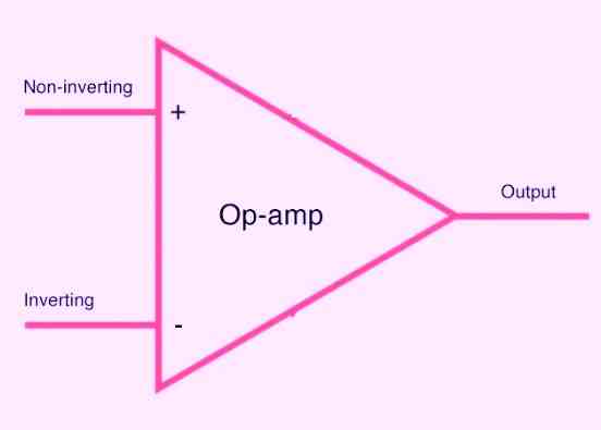
As shown in the figure above, the fundamental op amp is a three terminal device having two inputs and one output. The input terminals are classified as "inverting" or "non-inverting."
Op Amp Parameters
When supplied with equal input voltages, the output of the ideal operational amplifier, or "op amp," is zero, or "0 volts."
VIN 1 = VIN 2 gives VOUT = 0
Practical op-amps have an imperfectly balanced input, causing uneven bias currents to flow through the input terminals. In order to balance the op amp output, an input offset voltage must be provided between the two input terminals.
1) Input Bias Current
When the output is balanced, or when VOUT = 0, the input bias current (IB) is equal to one-half the total individual currents entering the two input connections. It is often a very tiny number; for example, IB = 100 nA is a normal value.
2) Input offset current
The difference between each individual current reaching the input terminals is known as the input offset current (Iio). Again, it is often of extremely low value; for instance, a common value is Iio = 10 nA.
3) Input offset voltage
In order to keep the op amp balanced, an input offset voltage Vio needs to be applied across the input terminal. Usually the value of Vio is = 1 mV.
Values of Iio and Vio may both vary with temperature, and this variation is referred to as Iio drift and Vio drift, respectively.
4) Power Supply Rejection Ratio (PSRR)
The ratio of the change in input offset voltage to the corresponding change in the power supply voltage is known as the power supply rejection ratio, or PSRR. This is often in the range of 10 to 20 uV/V.
Additional parameters for op-amps that might be mentioned are:
5) Open-loop gain/Closed loop Gain
Open-loop gain refers to an op-amp's gain without a feedback circuit, whereas closed-loop gain refers to an op-amp's gain with a feedback circuit. It is generally represented as Ad.
6) Common-mode rejection ratio (CMRR)
This is the ratio of the difference signal to the common-mode signal and serves as a measure of a differential amplifier's performance. We use Decibels (dB) to express this ratio.
The ideal operational amplifier (op-amp) generates an output that corresponds to the difference between the two signals applied to its input terminals, and it yields zero output when both inputs receive identical signals simultaneously, which is referred to as common mode operation.
However, in practical op-amps, common mode signals do not completely nullify, resulting in a small signal appearing at the op-amp's output terminal.
The op-amp's ability to reject these common mode signals is typically quantified using a parameter called the common mode rejection ratio (CMRR).
CMRR is defined as the ratio of the op-amp's gain with differential signals to its gain with common mode signals. Modern op-amps often exhibit CMRR values of around 90dB.
7) Slew Rate
Slew rate is the rate at which the output voltage of an amplifier changes under large signal conditions. It is represented using the unit V/us.
In addition to the conventional bandwidth restrictions, operational amplifiers (op-amps) are also susceptible to a phenomenon referred to as slew rate limitation.
This phenomenon imposes a constraint on the maximum rate of voltage change at the op-amp's output.
Slew rate is typically quantified in volts per microsecond, and commonly used op-amps typically have slew rate values ranging from 1V/μs to 10V/μs.
One consequence of slew rate limitation is that it provides a broader bandwidth for small output signals compared to larger output signals
8) Input Impedance Zin
This represents the input impedance observed when examining the input terminals of the operational amplifier in an open-loop configuration.
It is typically quantified solely in terms of resistance. For contemporary op-amps employing bipolar input stages, it's common to encounter values around 1M ohms, whereas field-effect transistor (FET) input types exhibit input impedances of one million megaohms or more.
9) Output Impedance Zo
This represents the output impedance of the fundamental operational amplifier when employed in an open-loop configuration. Typically, it is described solely in terms of resistance. Contemporary operational amplifiers often exhibit output impedance values in the range of a few hundred ohms.
10) Supply Voltage Range Vs
Operational amplifiers typically require power from two sets of supply rails, and it's crucial to ensure that these supply voltages stay within specified maximum and minimum thresholds.
Exceeding the upper limit can lead to potential damage to the op-amp, while falling below the lower limit can result in improper op-amp operation.
Commonly accepted supply voltage limits are typically in the range of ±3V to ±15V.
11) Input Voltage Range Vi(max)
It is imperative to ensure that the input voltage applied to the operational amplifier never surpasses the supply line voltages to prevent potential damage to the op-amp.
Typically, the maximum allowable input voltage, denoted as Vi(max), is specified to be one or two volts less than the supply voltage (Vs).
12) Output Voltage Range Vo(max)
When an operational amplifier is excessively driven, its output will reach saturation and become constrained by the provided supply voltages.
As a standard practice, the maximum achievable output voltage, denoted as Vo(max), is often specified to be one or two volts lower than the supply voltage (Vs).
13) Differential Input Offset Voltage Vio
In an ideal scenario, an op-amp would exhibit perfect alignment between its input and output terminals, with the output registering zero when both inputs are grounded.
However, practical op-amps fall short of this ideal, as minor imbalances within their input circuitry introduce a slight offset or bias voltage to the input terminals.
This is known as the DIFFERENTIAL INPUT OFFSET VOLTAGE, typically measuring just a few millivolts.
Nevertheless, when this voltage is magnified by the circuit's gain in which the op-amp operates, it can potentially drive the op-amp output to saturation.
As a result, most op-amps incorporate a means for externally compensating or nullifying this offset voltage.
14) Transition Frequency fT
An operational amplifier (op-amp) typically exhibits a low-frequency voltage gain of approximately 100dB.
To ensure stability, its open-loop frequency response is tailored in a way that reduces the gain as the frequency increases, eventually reaching a unity gain at a specific transition frequency referred to as "fT."
Typically, this response diminishes at a rate of 6dB per octave or 20dB per decade.
It's important to note that when the op-amp is utilized within a closed-loop amplifier circuit, the circuit's bandwidth is contingent upon the closed-loop gain.
For instance, if the amplifier is configured to provide a gain of 60dB, its bandwidth is limited to 1kHz. Conversely, if a gain of 20dB is set, the bandwidth extends to 100kHz.
Op Amp Basic Application Circuits
In the following paragraphs I have explained about several interesting op amp basic circuits. Each of the basic designs are explained with formulas to solve their component values and features.
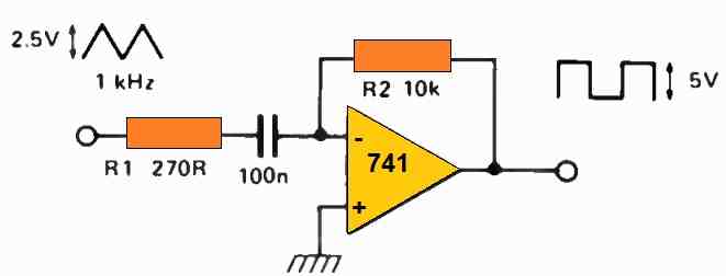
AMPLIFIER OR BUFFER
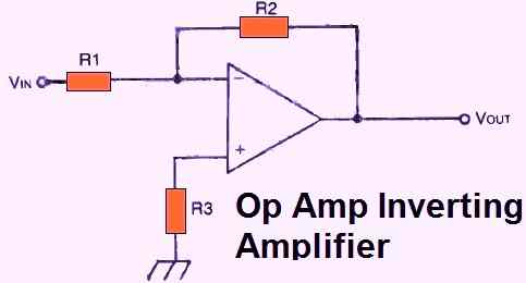
The circuit for an inverting amplifier, or an inverter, can be seen in Figure 1, above. The gain of the circuit is given by:
Av = - R2/R1
Note that the gain is negative one, indicating that the circuit operates as a phase-inverting voltage follower, if the two resistances are equal (i.e., R1 = R2). The output would be identical to the input, with the polarity reversed.
In reality, the resistors may be removed for unity gain and substituted by direct jumper wires, as shown in Fig. 2 below.
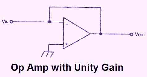
This is possible because R1 = R2 = 0 in this circuit. Typically, R3 is removed from the inverting voltage follower circuit.
The op amp output will amplify the input signal if R1 is less than R2. For instance, if R1 is 2.2 K and R1 is 22 K, the gain could be expressed as:
Av = - 22,000/2,200 = -10
The negative symbol denotes phase inversion. The input and output polarities are reversed.
By making R1 bigger than R2, the very same circuit may also attenuate (decrease the strength of) the input signal. For instance, if R1 is 120 K and R2 is 47 K, the circuit gain would be roughly:
Av = 47,000/120,000 = - 0.4
Again, the polarity of the output is the inverse of that of the input.
Although R3's value is not particularly important, it should be about equal to the parallel combination of R1 and R2. Which is:
R3 = (R1 x R2)/(R1 + R2)
To demonstrate this, consider our previous example, where R1 = 2.2 K and R2 = 22 K. R3's value in this situation should be approximately:
R3 = (2200 x 22000)/(2200 + 22000) = 48,400,000/24,200 = 2000 Ω
We can choose the closest standard resistance value for R3 because the precise value is not necessary. A 1.8 K or a 2.2 K resistor could be used in this case.
The phase inversion created by the circuit in Fig. 2 may not be acceptable in several situations.
To use the op-amp as a non-inverting amplifier (or like a simple buffer), connect it as illustrated in Fig. 3 below.
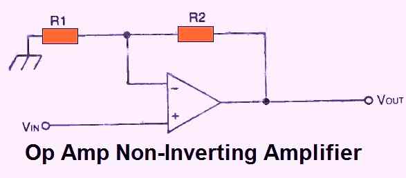
The gain in this circuit is expressed as follows:
Av = 1 + R2/R1
The output and input have the same polarity and are in phase.
Keep in mind that the gain must be always at minimum 1 (unity). It is not possible to attenuate (reduce) signals using a non-inverting circuit.
The gain of the circuit will be comparatively stronger if R2 value is significantly greater than R1. For instance, if R1 = 10 K and R2 = 47 K, the gain of the op amp will be as given below:
Av = 1 + 470,000/10,000 = 1 + 47 = 48
However, if R1 is significantly bigger than R2, the gain will only be somewhat more than unity. For example, if R1 = 100 K and R2 = 22 K, the gain would be:
Av = 1 + 22,000/100,000 = 1 + 0.22 = 1.22
In case the two resistances are identical (R1 = R2), the gain would always be 2. To convince yourself of this, try the gain equation in a few scenarios.
A specific situation is when both resistances are set to 0. In other words, as seen in Fig. 4 below, direct connections are used in place of the resistors.
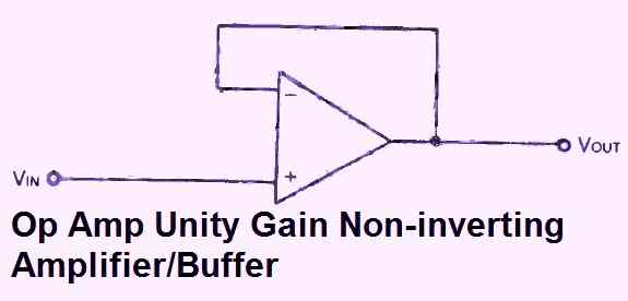
The gain is exactly one in this case. This conforms to the gain formula:
Av = 1 + R2/R1 = 1 + 0/0 = 1
The input and the output are identical. Applications for this non-inverting voltage follower circuit include impedance matching, isolation, and buffer.
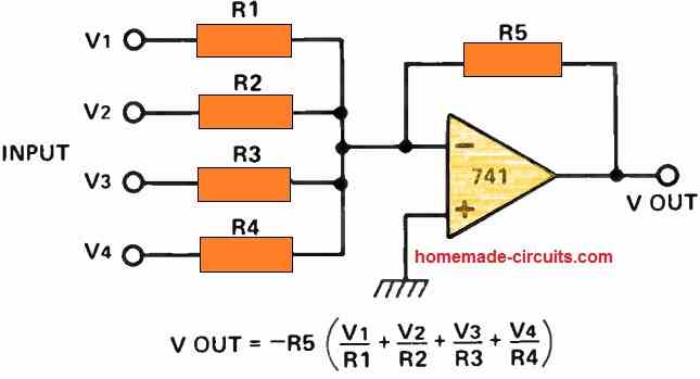
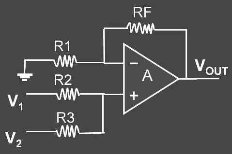
ADDER (Summing Amplifier)
A number of input voltages could be added using an op amp. As illustrated in Fig. 5 below, input signals V1, V2,… Vn are applied to the op amp via resistors R1, R2,… Rn.
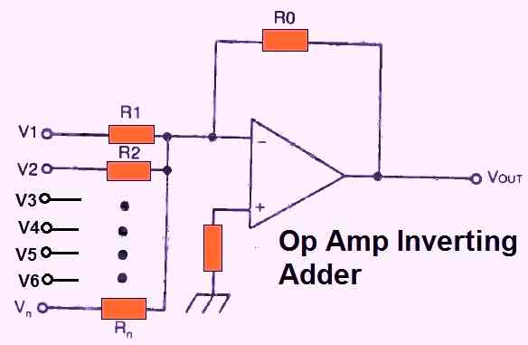
These signals are then combined to produce the output signal, which equals the sum of the input signals. The following formula may be used to calculate the op-amp's real performance as an adder:
VOUT = - Ro ((V1/R1) + (V2/R2) . . . + (Vn/Rn))
See the negative symbol. This means that the output has been inverted (the polarity is reversed). In other words, this circuit is an inverting adder.
The circuit may be changed to function as a non-inverting adder by switching the connections to the op-amp's inverting and non-inverting inputs, as illustrated in the figure below.
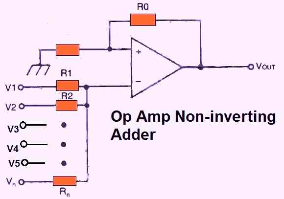
The output equation could be made simpler by assuming that all of the input resistors have identical values.
VOUT = - Ro ((V1 + V2 . . . + Vn)/R)
Practical Op amp Audio Mixer Amplifier
A virtual ground amplifier serves as a versatile tool for blending multiple signals into a unified output. The resultant output voltage comprises a combination of all the input signals.
The extent to which a particular input signal influences the output is inversely linked to the input resistor's value.
When the input voltages are channeled through potentiometers before reaching the mixer, it enables manual adjustment of their individual levels.
This forms the fundamental principle behind many audio mixers, albeit less expensive units tend to employ operational amplifiers (op-amps).
It's worth noting that most op-amp-based mixers tend to compromise the signal-to-noise ratio of the input signals more than a high-quality discrete component amplifier would.
DIFFERENTIAL AMPLIFIER
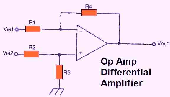
Fig. 7 above depicts the basic circuit of a differential amplifier using an op amp. The component values are set so that R1 = R2 and R3 = R4.
Therefore, performance of the circuit can be calculated using the following formula:
VOUT = VIN 2 - VIN 1
Only as long as the op amp can accept that inputs 1 and 2 have different impedances (input 1 has an impedance of R1 and input 2 has an impedance of R1 plus R3).
ADDER/SUBTRACTOR
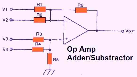
Figure 8 above depicts the configuration for an op amp adder/subtractor circuit. In the event when R1 and R2 have the identical values and R3 and R4 are likewise set to the same values, then:
VOUT = (V3 + V4) - (V1 - V2)
In other words, Vout = V3 + V4 is the total of the V3 and V4 inputs while it is the subtraction of the V1 and V2 inputs.
The values for R1, R2, R3, and R4 are selected to match the characteristics of the op amp. R5 should be equal to R3 and R4, and R6 should be equal to R1 and R2.
MULTIPLIER
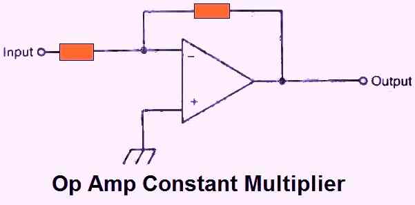
Simple multiplication operations may be done with the basic op amp circuit seen in Fig. 9 above. Keep in mind that this is the same circuit as in Fig. 1.
To achieve a consistent gain (and subsequently a multiplication of the input voltage in the ratio R2/R1) and precise results, precision resistors with the prescribed values for R1 and R2 should be used.
Notably, the output phase is inverted by this circuit. The voltage at the output will be equal to:
VOUT = - (VIN x Av)
where Av is the gain, as determined by R1 and R2. VOUT and VIN are the output and input voltages, respectively.
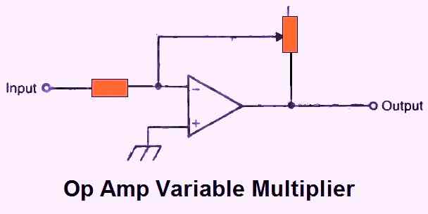
As seen in Fig. 10 above, the multiplication constant can be altered if R2 is a variable resistance (potentiometer).
Around the control shaft you can mount a calibration dial with marks for various common gains. The multiplication constant may be read directly from this dial using a calibrated reading.
INTEGRATOR
An op-amp will, at the very least, theoretically function as an integrator when the inverting input is coupled with the output through a capacitor.
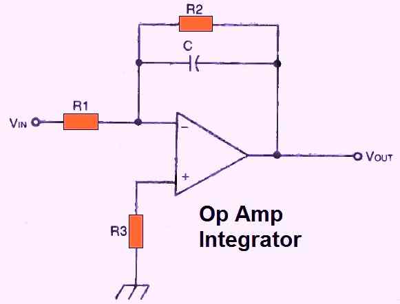
As indicated in Fig. 11 above, a parallel resistor must be connected across this capacitor in order to maintain DC stability.
This circuit implements the following relationship to integrate input signal:
R2's value should be selected to match the op amp parameters, such that:
VOUT = R2/R1 x VIN
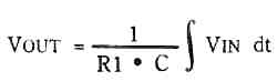
Practical Integrator Circuit
As shown in the following figure, an operational amplifier (op-amp) in conjunction with a capacitor offers a highly precise means of implementing mathematical integration. In this scenario, we accumulate current over a period, resulting in a generated voltage that represents the integral of that current with respect to time.
Essentially, if a constant voltage is applied to the circuit, it produces an output in the form of a ramp with a consistent slope.
When the input voltage is positive, the op-amp's output undergoes a negative ramp.
This action causes the inverting terminal to move negatively, thereby preserving a 'virtual earth' condition. In reality, the input current (Vin/R1) equals the current flowing through the capacitor, thus ensuring equilibrium.
The governing equation for capacitor behavior is C x dV/dt =, where dV/dt signifies the rate of voltage change across the capacitor.
Therefore, dV/dt = i / C, which can be further expressed as dV/dt = Vin / R1 x C.
Consequently, when a square wave is applied to the aforementioned circuit, it generates triangular waveforms.
To enhance DC stability, we introduced R2. While its inclusion does introduce some minor deviations in the mathematical processes, the impact is not substantial.
An advantageous feature of this integrator design is its remarkably low output impedance. Even when a load is connected to the output, the op-amp consistently produces the same waveform, underscoring the effectiveness of negative feedback.
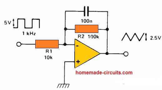
DIFFERENTIATOR
The differentiator op amp circuit includes a capacitor in the input line that connects to the inverting input and a resistor that connects this input to the output.
However, this circuit has clear limits, therefore a preferable setup would be to parallel the resistor and capacitor as illustrated in Fig. 12 above.
The following equation determine how well this circuit performs:
VOUT = - (R2 x C1) dVIN/dt
Practical Differentiator Circuit
The following figure shows a practical op amp differentiator circuit with part numbers.
From a mathematical perspective, differentiation stands as the inverse operation of integration. Consequently, in a differentiator circuit, the roles of C (capacitor) and R (resistor) are reversed compared to an integrator circuit.
The input waveform is a triangle wave characterized by a steady incline and decline. This consistent slope, when applied to a capacitor, results in the generation of a constant current.
As the slope direction reverses, the current flow also reverses. This changing current, when directed through a resistor (R1), subsequently produces a square wave.
LOG AMPLIFIERS
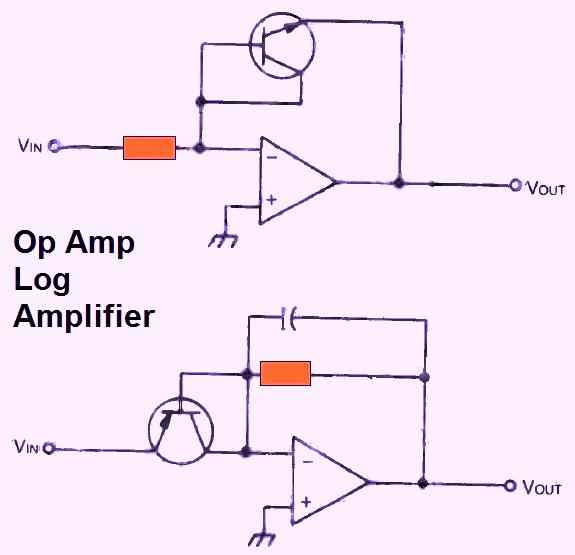
The fundamental op amp circuit (Fig. 13 above) employs an NPN transistor and an op-amp to generate an output proportional to the input's log:
VOUT = (- k log10) VIN/RIo
The "inverted" circuit, working as a fundamental anti-log amplifier, is depicted in the lower diagram. Typically, the capacitor is of low value (e.g., 20 pF).
AUDIO AMP
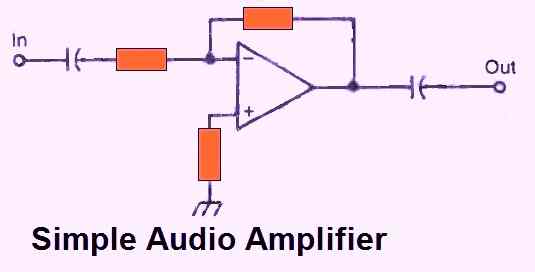
An op amp, is essentially a dc amplifier but may also be applied for ac applications. A straightforward audio amplifier is shown in Figure 14 above.
AUDIO MIXER
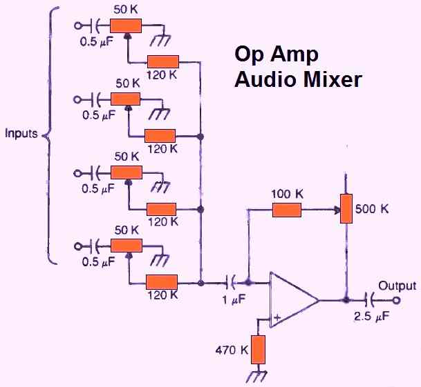
A modification of the audio amplifier is shown in this circuit (Fig. 15 above). You can see how it resembles the adder circuit in Fig. 5.
The different input signals are blended or merged. Each input signal's input potentiometer allows for level adjustment.
The relative proportions of the different input signals in the output can thus be adjusted by the user.
SIGNAL SPLITTER
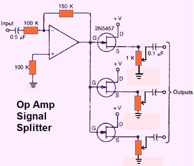
The signal splitter circuit seen in Fig. 16 above is just the opposite of a mixer. A single output signal is divided into several identical outputs that feed various inputs.
The multiple signal lines are separated from one another using this circuit.
To adjust the required level, each output line includes a separate potentiometer.
VOLTAGE TO CURRENT CONVERTER
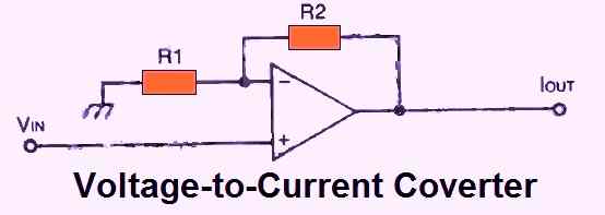
The circuit presented in Fig. 17 above will cause the load impedance R2 and R1 to experience the same current flow.
This current's value would be proportional to the input signal voltage and independent of the load.
However, due to the high input resistance provided by the non-inverting terminal, the current will be of relatively low value.
This current has a value that is directly proportional to VIN/R1.
Practical Voltage to Current Converter using an Op Amp
Combining the virtual ground concept of an operational amplifier (op-amp) with the current sourcing capability of a transistor allows for the creation of a high-precision linear voltage-to-current converter.
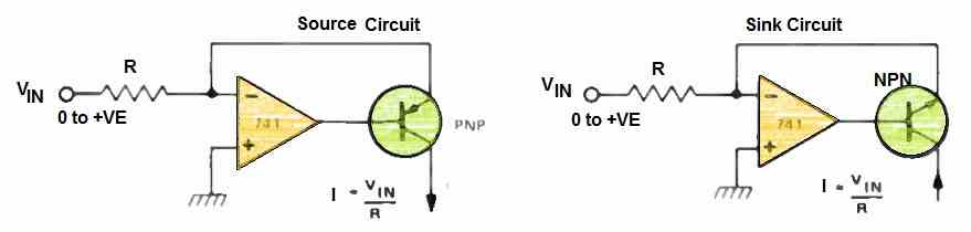
Let's delve into the 'SOURCE' circuit.
When a positive voltage is applied, the op-amp self-adjusts to maintain a 'virtual ground' state.
Consequently, a current denoted as 'i' flows through the input resistor 'R,' with 'i' equal to 'Vin/R.' Now, this current needs a path, so it travels through a PNP transistor, exiting via the collector and entering its designated load.
Consequently, the input voltage generates a current linearly proportional to it.
However, three factors introduce potential errors that affect this linearity. First, at lower Vin levels, the op-amp's input offset voltage might become significant.
Second, when Vin is low, the input bias current may substantially deplete the available current. Third, the base current of the transistor must be subtracted from the final output current.
It's crucial to note that the transistor's current gain varies with collector current changes, making the base current loss non-constant.
Nevertheless, a precise voltage-to-current converter can be achieved using an op-amp with a FET (Field-Effect Transistor) input to minimize bias current.
Additionally, an input balance can be utilized to nullify the input offset voltage, and replacing the bipolar transistor with a FET can eliminate the base current issue.
The 'SINK' circuit essentially swaps the transistor for an NPN type, necessitating a negative input voltage.
CURRENT TO VOLTAGE CONVERTER
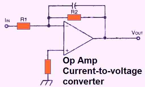
If the output voltage is equal to IIN x R2 and the design (Fig. 18 above) is used, the input signal current can flow straight via the feedback resistor R2.
To put it another way, input current is transformed into a proportionate output voltage.
The bias circuit created at the inverting input sets a lower limit on current flow, which prevents any current from passing through R2.
To eliminate "noise," a capacitor can be added to this circuit as illustrated in the figure.
CURRENT SOURCE
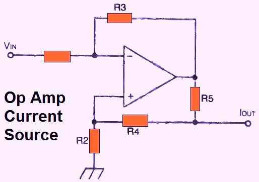
The above figure 19 shows how an op amp can be used like a current source. The resistor values can be calculated using the following equations:
R1 = R2
R3 = R4 + R5
The output current can be evaluated using the following formula:
Iout = (R3 x VIN) / (R1 x R5)
MULTIVIBRATOR
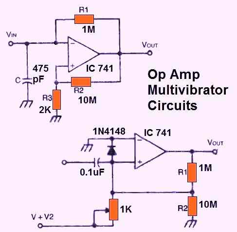
You may adapt an op amp to use as a multivibrator. Fig. 20 above displays two fundamental circuits.
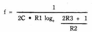
The design at the top left is a free running (astable) multivibrator, whose frequency is controlled by:
A monostable multivibrator circuit that can be activated by a square wave pulse input could be seen in the lower right diagram. The component values provided are for a CA741 op amp.
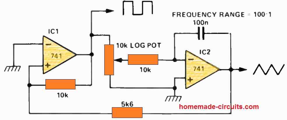
Single Op Amp Oscillator
The next straightforward electronic circuit incorporates a Schmitt trigger and a quasi-integrator, all constructed around a single operational amplifier (op-amp).
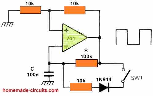
Positive feedback is established through the use of 10 k ohm resistors. The "integration" or timing aspect is regulated by the RC network.
The voltage at the inverting input traces the exponential charging curve of the RC network, with the exception that it is constrained within the upper and lower hysteresis boundaries.
As a result, the hysteresis levels and the RC time constant jointly dictate the operational frequency. It is feasible to achieve a significantly high mark-to-space ratio in the output square wave.
When switch SW1 is activated, the capacitor's discharge time accelerates elevenfold compared to the rise time. Consequently, this configuration generates a square wave with an impressive 11:1 mark-to-space ratio.
SQUARE WAVE GENERATOR
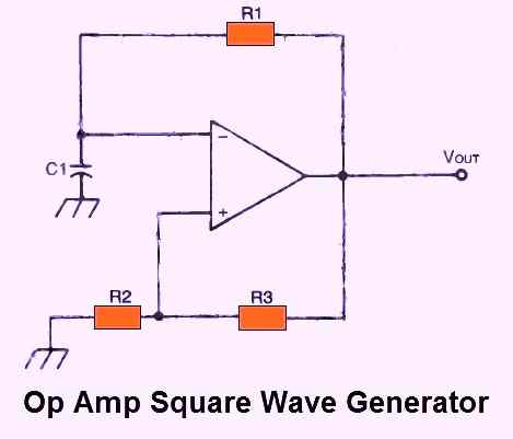
Fig. 21 above depicts a functional square wave generator circuit centered around an op amp. This square wave generator circuit could possibly be the most straightforward one. Just three external resistors and one capacitor are needed in addition to the op amp itself.
The two main elements that determine the circuit's time constant (output frequency) are the resistor R1 and the capacitor C1.
However the R2 and R3-based positive feedback connection also has an impact on the output frequency.
Although equations are often somewhat complicated, they can be made simpler for particular R3/R2 ratios. For illustration:
If R3/R2 ≈ 1.0 then F ≈ 0.5/(R1/C1)
or,
If R3/R2 ≈ 10 then F ≈ 5/(R1/C1)
The most practical method is to employ one of these standard ratios and change the values of R1 and C1 to achieve the required frequency.
For R2 and R3, conventional values may be employed. For instance, the R3/R2 ratio will be 10 if R2 = 10K and R3 = 100K, thus:
F = 5/(R1/C1)
In most cases, we will already be aware of the required frequency, and we will only need to choose the appropriate component values.
The simplest method is to first choose a C1 value that seems reasonable, and then rearrange the equation to find R1:
R1 = 5/(F x C1)
Let's look at a typical example of 1200 Hz frequency we're looking for. If C1 is connected to a 0.22uF capacitor, then R1 should have the value as depicted in the following formula:
R1 = 5/(1200 x 0.00000022) = 5/0.000264 = 18,940 Ω
A typical 18K resistor might be employed in the majority of applications.
A potentiometer may be added in series with R1 to increase the usefulness and adaptability of this circuit, as illustrated in Fig. 22 below. This makes it possible to manually adjust the output frequency.
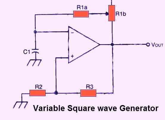
For this circuit, the very same calculations are used, however R1's value is changed to match the series combination of the fixed resistor R1a and the adjusted value of the potentiometer R1b:
R1 = R1a + R1b
The fixed resistor is inserted to ensure that the value of R1 never drops to zero. The range of output frequencies is determined by the fixed value of R1a and the highest resistance of R1b.
VARIABLE PULSE WIDTH GENERATOR
A square wave is totally symmetrical. The square wave signal's duty cycle is defined as the ratio of high level time to total cycle time. Square waves have a 1:2 duty cycle by definition.
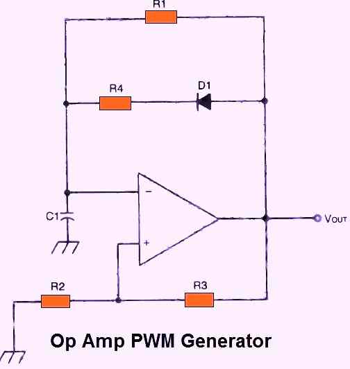
With just two more components, the square wave generator from the previous section may be transformed into a rectangle wave generator. Fig. 23 above depicts the updated circuit.
Diode D1 restricts the passage of current via R4 on negative half cycles. R1 and C1 make up the time constant as expressed in the following equation:
T1 = 5/(2C1 x R1)
However, on positive half-cycles, the diode is allowed to conducts, and the parallel combination of R1 and R4 along with C1 defines the time constant, as shown in the following calculation:
T2 = 5/(2C1 ((R1 R4)/(R1 + R4)))
The overall cycle length is just the total of the two half-cycle time constants:
Tt = T1 + T2
The output frequency is the inverse of the total time constant of the whole cycle:
F = 1/Tt
Here the duty cycle will not equal 1:2 because the time constant for the high and low level sections of the cycle will differ.
Asymmetrical waveforms will be produced as a result. It is possible to make R1 or R4 adjustable, or even both of them, but be aware that doing so would change both the output frequency and duty cycle.
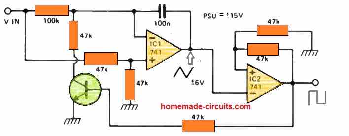
Triangle and Square Wave Generator Circuit
A dependable oscillator capable of generating both triangle and square waveforms can be assembled using a Schmitt trigger and an integrator, as shown in the following diagram. The operation of this basic op amp circuit is straightforward and reliably self-starting. The Schmitt trigger is constructed from IC1, while IC2 forms the integrator.
Suppose the Schmitt trigger's output is positive. This prompts the integrator to produce a descending negative ramp. This ramp is then fed back to the input of the Schmitt trigger.
Once the lower hysteresis level is reached, the Schmitt trigger's output swiftly switches to its negative state.
This shift results in the withdrawal of current from the integrator, which subsequently produces an ascending positive ramp.
The integrator's output oscillates between the upper and lower hysteresis levels. The speed at which the integrator oscillates is determined by the voltage magnitude applied to it.
In this particular circuit, the voltage magnitude, and consequently the oscillation frequency, are regulated by a potentiometer, providing a control range spanning 100 to 1.
This circuit forms the foundation of most function generators. By modifying the triangle waveform, it is feasible to approximate a sine wave.
With some additional electronic components, it is also possible to make the oscillator voltage-controlled.
SIMPLE TRIANGLE TO SINEWAVE CONVERTER
Here's an uncomplicated method for transforming a triangular waveform into a sinusoidal one, using a single op amp.
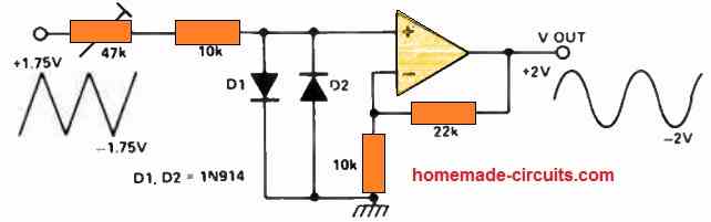
This technique relies on harnessing the logarithmic properties of diodes to mimic the sinusoidal curve. The resulting distortion levels hover around 5% or thereabouts.
Nevertheless, this level of distortion might be deemed acceptable when the sinusoidal waveform serves solely as a source for generating audio tones.
Voltage Controlled Oscillator
The following op amp oscillator closely resembles the triangular square wave oscillator demonstrated on this page, with the key distinction being its voltage-controlled nature.
The integrator and Schmitt trigger functions remain consistent with the previous design, but the feedback mechanism has undergone modification.
The input voltage, denoted as Vin, is differentially applied to the integrator through a resistor network.
The magnitude of Vin directly influences the rate at which the integrator ascends and descends.
Consequently, the operating frequency is contingent upon an external positive control voltage, and this voltage imparts a linear influence on the frequency.
When the Schmitt trigger's output is low, Q1 remains in the off state, allowing the entire input voltage to be applied to the inverting input.
Simultaneously, half of the input voltage consistently applies to the non-inverting input. Consequently, the integrator's output descends until the Schmitt trigger switches to its positive state.
At this point, Q1 becomes active, rendering the voltage at the inverting input negative relative to the non-inverting input. Consequently, the integrator's output commences an upward trajectory.
SINE WAVE OSCILLATOR
The sine wave, which is shown in the figure below, is the most basic of all ac signals.
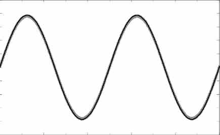
There is absolutely no harmonic content in this extremely pure signal. There is just one fundamental frequency in a sine wave.
Actually, creating a completely pure, distortion-free sine wave is rather difficult.
Thankfully, using an oscillator circuit built around an op-amp, we can get pretty near to an optimal waveform.
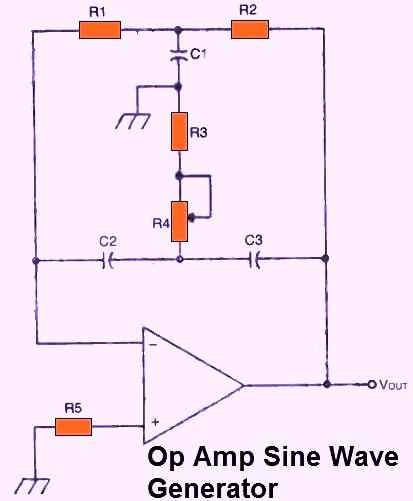
Figure above above depicts a conventional sine wave oscillator circuit incorporating an op-amp. A twin-T circuit serving as a band-reject (or notch) filter serves as the feedback network.
The capacitor C1 and the resistors R1 and R2 make up one T. C2, C3, R3, and R4 make up the other T. The schematic has it reversed. The component values must have the following relationships for this circuit to work properly:
The following formula determines the output frequency:
F = 1/(6.28 x R1 x C2)
By changing R4's value, the twin-T feedback network tuning could be tweaked somewhat. Typically, this could be a tiny trimmer potentiometer.
The potentiometer is set to its highest resistance and then gradually reduced until the circuit just hovers on the verge of oscillation. The output sine wave might get corrupted if the resistance is adjusted too low.
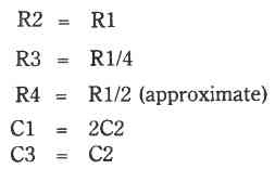
SCHMITT TRIGGER
Technically speaking, a Schmitt trigger may be referred to as a regenerative comparator. Its primary function is to transform an input voltage that is slowly changing into an output signal, at a particular input voltage.
To put it another way, it has a "backlash" property called hysteresis which functions like a voltage "trigger."
The op amp becomes the basic building block for the Schmitt trigger operation (see Fig. 26 above). The following factors determine the triggering or trip voltage:
Vtrip = (Vout x R1) / (-R1 + R2)
In this type of a circuit, the hysteresis is double the trip voltage.
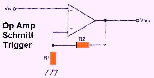
In Fig. 27 below, another Schmitt trigger circuit is depicted. In this circuit, the output is said to be "triggered" when the dc input hits about one-fifth of the supply voltage.
The supply voltage may be anywhere between 6 and 15 volts, therefore depending on the supply voltage chosen, the trigger can be set to operate at 1.2 to 3 volts.
If necessary, the actual triggering point could also be altered by modifying the value of R4.
The output will be the same as the supply voltage as soon as it is triggered.
If the output is attached to an incandescent bulb or LED (through a series ballast resistor), the lamp (or LED) will illuminate once the input voltage hits the triggering value, indicating that this precise voltage level has been achieved at the input.
BUFFERED VOLTAGE REFERENCE GENERATOR POJECT
This useful little circuit compels the output of the opamp to be set at a value defined by the supply voltage and the voltage divider made up of RI and R2.
By using this functionality, you could provide other circuits a constant bias voltage reference. In the example, the output voltage is equal to 50% of the input voltage.
The 50% or 1/2 the supply voltage value at the output is due to the use of identical resistors for R1 and R2.
You could change the R1 and R2 values to get any other desired output reference voltage. The output is fully buffered by the op amp.
BURGLAR ALARM CIRCUIT PROJECT USING a SINGLE OP AMP
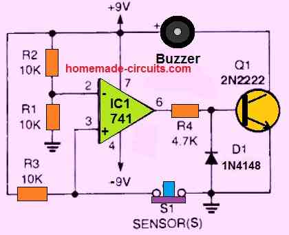
This circuit uses an op amp to configure a closed loop alarm system with a buzzer.
The inverting input of the op amp is rigged at 1/2 the supply voltage, while the non-inverting input is connected to the ground line through a "normally-closed" push button switch.
This switch works like a intruder detector.
In the above situation while the switch is depressed and closed, the output of the op amp is low or at zero volts.
When a potential burglar or an intruder steps over the switch, the switch opens. As soon as this happens, the non-inverting input pin#3 of the IC goes higher than the pin#2 potential.
Due to this the output of the op amp turns high equal to the supply DC level and it sounds the alarm or the connected buzzer.
A large value capacitor could be connected across the base/emitter of the 2N2222 to ensure that the buzzer keeps sounding even after the push switch is returned to its original condition.
PEAK VOLTAGE DETECT AND HOLD
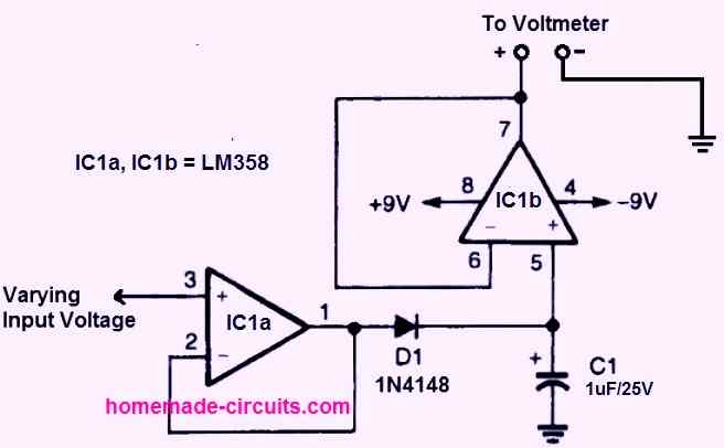
Our next basic op amp circuit will detect the peak value of a varying input voltage, and then hold it so that the peak level can be analyzed with a meter.
Opamp IC1a is wired as a high impedance voltage follower circuit. This is because its positive input pin 3 is linked to the modulating input signal.
When the input voltage reaches its maximum value, the peak voltage is applied across C1, charging it to the maximum.
Diode D1 prevents the voltage from discharging back into IC1a by allowing only the positive peak voltage to reach C1.
Opamp IC1b is another voltage follower and generates the maximum output at pin #7. This may be evaluated using a digital or analogue voltmeter.
Now, as the input level begins dropping below the peak value, C1 begins to discharge gradually. To obtain the most precise peak reading, the output measurement must be carefully monitored.
Basic Sample and Hold Circuit using Op Amp and FET
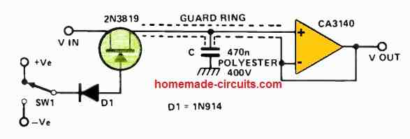
Creating a fundamental op amp circuit that can effectively sample an analog voltage and retain it over an extended period without significant voltage degradation is commonly known as a sample and hold circuit.
One practical application of such a circuit is storing the voltage input received from a keyboard connected to an electronic music synthesizer.
This stored voltage is subsequently utilized to control the pitch of a voltage-controlled oscillator, emphasizing the critical importance of a high-performance sample and hold circuit.
It is imperative that the voltage drift remains below one semitone (equivalent to 80 mV) over a ten-minute span.
In its essence, a sample and hold circuit comprises a straightforward configuration, consisting of an electronic switch, a storage capacitor, and a high-input impedance voltage follower.
In the depicted circuit, when switch SW1 is in the positive position, it activates the Field-Effect Transistor (FET), which exhibits an approximate resistance of 400 ohms.
Consequently, the input voltage charges the capacitor through the FET. Conversely, when SW1 is switched to the negative state, the FET is turned off (pinched off), resulting in a resistance that can reach thousands of megohms.
To achieve an extended storage duration, it is essential for the operational amplifier (op-amp) to possess an exceedingly low input bias current.
For instance, the CA3140 op-amp typically exhibits a bias current of around 10 picoamps (10-11 amps).
To estimate the rate at which the capacitor discharges due to this current, we can apply the equation C(dv/dt) =, where dv/dt represents the rate of voltage change on the capacitor.
Thus, dv/dt = I / C = 10-11 / (0.47 x 10⁻⁶) = 22 microvolts per second (uV/sec). This low drift rate exceeds the necessary requirements.
However, the actual drift rate is likely to surpass this theoretical value due to factors such as surface leakage on the printed circuit board, leakage through the FET, and internal leakage within the capacitor.
To minimize leakage currents, it is advisable to employ a high-voltage, non-polarized capacitor in the circuit.
Additionally, a simple PCB technique can be implemented to prevent surface leakage by creating a guard ring around the sensitive components.
Typically, any charge stored on the capacitor may leak to the ground via the PCB's surface.
However, by establishing a conducting track around the sensitive area and maintaining it at the same potential as that of the capacitor, the potential difference remains virtually zero, significantly reducing surface leakage.
Basic Timer Circuit Project using Op amps
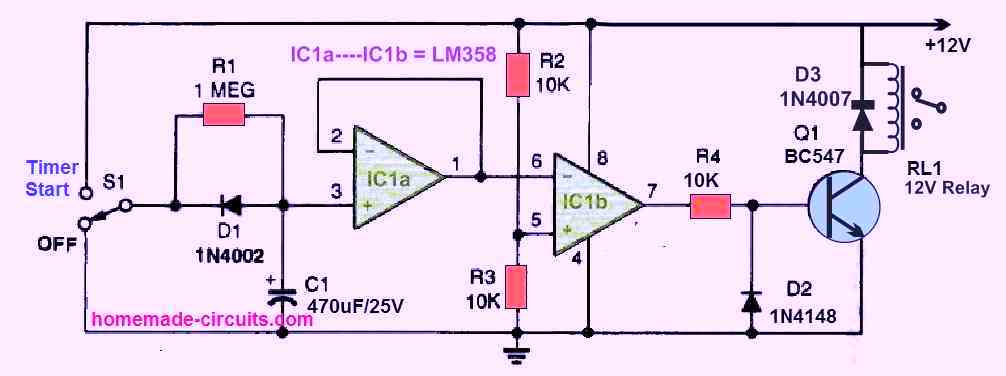
Our next design is a basic op amp based timer circuit. A couple of op amps IC1a and IC1b from the IC LM358 can be seen in the circuit.
IC1a is configured as a voltage follower and the basic timer circuit. IC1b is configured in a detector/comparator arrangement.
When the switch S1 in the OFF position, the pin#3 of IC1a remains grounded or at zero volts. IC1a being a voltage follower replicates its input zero volt at its output pin#1. Thus pin#1 also stays at 0V.
This causes pin#6 of IC2 to remains at 0V, causing the non-inverting pin#5 to remain at a higher potential than pin#6.
Since IC1b is rigged as a comparator, a higher potential at pin#5 causes its output to go high.
This in turn allows the transistor and the relay to remain switched ON. In this situation the load also remains switched ON.
To start the timer action we have to now move the S1 to the "start timer" position.
As soon as S1 is moved to "start timer" position, C1 begins charging via R1. The potential at pin#3 of IC1a now slowly starts rising and the same is replicated on its pin#1 and pin#6 of IC1b.
Resistor R2 and R3 being identical ensures that the potential at pin#5 of IC1b is fixed 1/2 of the supply voltage. Meaning, the potential at pin#5 will be 6 V.
Now, as C1 charges the potential at pin#6 also rises slowly, until it exceeds the 6 V mark. When the pin#6 potential exceeds the pin#5 potential, the output of IC1b pin#7 instantly turns low or 0V.
When this happens the transistor Q1 is switched OFF. This likewise switches of the relay and the connected load.
The value of R1 and C1 can be tweaked as desired to change the timing period from a few seconds to many minutes.
MOTOR SPEED AND DIRECTION CONTROLLER USING A SINGLE OP AMP
The next project above is a very fundamental op amp circuit which not only regulates the speed of a motor, but also determines its direction of rotation.
The op-amp here is yet again configured in a voltage follower mode. Its positive input at pin #3 hooked up with the pot R3 which serves as a motor speed controller and also as a direction controller.
The output of the op-amp will be close to zero whenever the wiper of the pot R3 is in the middle of its range. In this position neither Q1 nor Q2 is switched on.
The op amp output turns positive as soon as the pot wiper is moved toward the positive side. When this happens and Q1 begins transferring current to the motor.
The output of the op-amp swings to a negative voltage when the potentiometer is adjusted toward the negative supply, shutting off Q1 and turning on Q2. This action also changes the rotating direction of the motor.
The speed of the motor rises in the direction it is spinning, depending on how far the R3 wiper is pulled toward either end of the potentiometer.
To find the maximum DC voltage range acceptable for the selected motor, you may have to monitor the voltage variation on emitters of Q1 and Q2.
SIMPLE MICROPHONE AMPLIFIER
Our next basic op amp circuit project can be seen in the above figure. It is an electret condenser microphone amplifier circuit.
In this design, the op amp is operated in an inverted adjustable gain amplifier circuit with a low potential electret microphone feeding the input.
Take note that this amplifier circuit is powered by a single 9-volt source (which also provides a necessary level of DC via the microphone).
Using potentiometer R4, you may change the gain of the circuit from a low gain of 10 to a high gain of 110 (when R4 is adjusted to its maximum resistance of 100k -ohm).
Basic 12 V Regulated Power Supply Circuit Project
The substantial open-loop voltage amplification of an operational amplifier (op-amp) proves highly advantageous for establishing a 12 V stable power supply with a low output impedance.
To create a 5.1V voltage reference, we employ a zener diode labeled as ZD1. Enhancing the stability of this voltage reference can be achieved by operating it under constant current conditions.
In this setup, a PNP transistor serves as a series regulator, albeit with signal inversion from the op-amp output. To introduce negative feedback, we connect the feedback to the non-inverting input.
The operational sequence unfolds as follows: The inverting input is held at 5.1V. Should the 'PSU OUTPUT' attempt to decrease, it causes a drop in voltage at the non-inverting input.
Consequently, the op-amp's output voltage also decreases, turning on the PNP transistor. This action, in turn, elevates the 'PSU OUTPUT,' effectively stabilizing the output voltage.
Furthermore, this negative feedback ensures that the output impedance remains exceptionally low. At higher frequencies where the op-amp's gain is diminished, the output impedance is further diminished by the inclusion of a 10 µ capacitor.
To maximize the available voltage output from the system before an unstable unregulated power supply threatens the regulated supply's integrity, we've incorporated a 5.1V zener diode (ZD2).
This configuration permits the op-amp output to operate at approximately 7 volts below the unregulated power supply rail.
Consequently, a regulated output persists until the PNP transistor reaches saturation.
Remarkably, this allows the unregulated rail to dip to within about 200 mV of the regulated rail without compromising the regulated output.
Op amp Speech Filter Circuit
The telephone network was meticulously crafted to facilitate verbal communication. After extensive years of experimentation, the system's bandwidth was determined to be in the range of 300 Hz to 3400 Hz.
Consequently, it can be affirmed that a significant portion of the meaningful information in spoken language resides within these frequency boundaries.
The diagram illustrates a filter configuration designed to emulate the telephone's bandwidth characteristics.
This filter structure holds versatile potential, serving various purposes such as acting as a "speech filter" to enhance clarity in noisy radio reception or landline conversations.
Additionally, it can function as a voice detection mechanism for applications like light shows.
Musical Chime Generator Circuit
The following basic op amp schematic represents a multiple feedback band-pass filter. A preset component is employed to introduce positive feedback, thereby enhancing the Q factor.
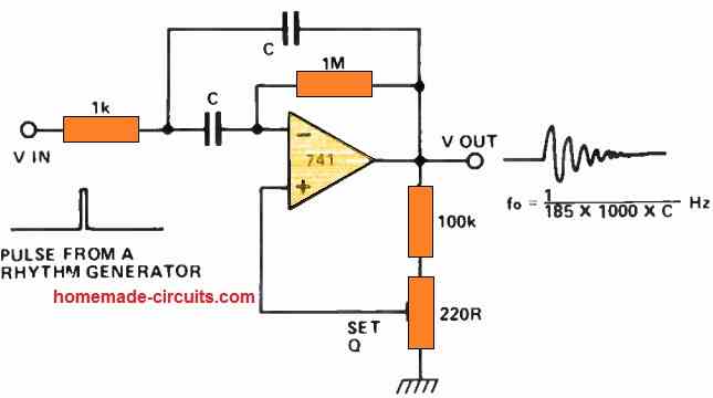
The operational principle is as follows: a brief pulse or click is applied to the filter, causing it to resonate naturally at its resonance frequency.
These oscillations subsequently decay exponentially over time, closely resembling various percussive or plucked sounds found in nature.
The duration of the decay time constant is directly related to the value of the C1 component; higher values of C1 result in longer decay times.
Higher-frequency resonances tend to resemble chiming sounds, while lower frequencies produce sounds akin to claves or bongos.
By configuring several of these circuits, each with distinct tuning, to be triggered by pulses from a rhythm generator, it is possible to create an intriguing array of sound patterns.
However, it's worth noting that stability issues may arise when operating at high Q or high frequencies.
To enhance performance, one can opt for an operational amplifier with a wider bandwidth than the 741, or consider an alternative filter structure like a state-variable filter. The latter option can yield Q values of up to 500.
Noise Free Audio Switching Circuit
At times, there arises a need for electronic switches to manage audio signals. While FETs can be employed for this purpose, they have some drawbacks, including potential distortion, relatively high resultant output impedance, and the possibility of clicking noises permeating through during switching events. The depicted circuit effectively addresses and mitigates these issues.
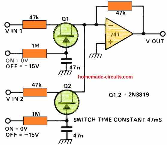
By utilizing an operational amplifier (op-amp), the circuit achieves an exceptionally low output impedance and affords the flexibility to select or blend one or more input channels.
The virtual ground mixing approach ensures that the voltage across any activated FET remains minimal.
For instance, if the output voltage is 1V and the ON resistance of the FET is 470 ohms, the voltage across the FET amounts to approximately 10 mV. In cases where substantial voltages are applied to an active FET, distortion can be significant.
However, when the voltage is kept small, around 10 mV, the distortion can be reduced to less than 0.1%. Consequently, virtual ground mixing facilitates low-distortion operation.
To eliminate the occurrence of switching clicks, a time constant of 47 milliseconds has been enforced at the gate of the FETs.
Increasing Slew Rate of an Op Amp
Enhancing the op-amp's slew rate can be achieved through the augmentation of its current generating capacity by introducing a pair of transistors.
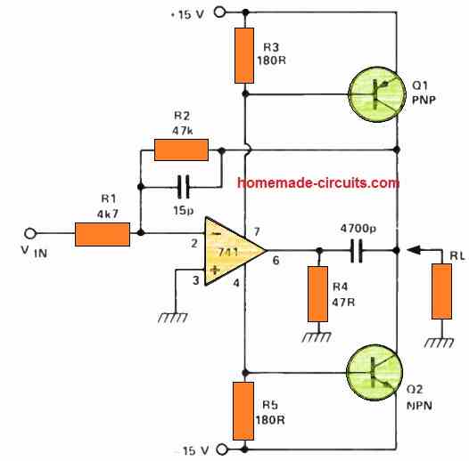
These transistors expand the output voltage range, permitting voltage swings within a 0.5V margin of either supply rail. Consequently, the op-amp's output remains nearly stationary.
In the absence of an input signal, the output voltage sits at 0V, drawing approximately 2mA from the supply rails. This current traverses the 180-ohm resistors, establishing a voltage level just shy of activating either transistor.
Upon applying a positive input voltage, the op-amp endeavors to shift towards the negative region.
However, a 47-ohm resistor (R4) connects its output to ground. Consequently, as it attempts this negative swing, it draws a substantial amount of current from the negative rail.
This current flows through R5, activating Q2 in the process. Q2, in turn, pulls down R2, thereby facilitating negative feedback.
A similar sequence of events unfolds when a negative input voltage is applied, albeit with the involvement of R3 and Q1. In this manner, the robust current capabilities of discrete transistors combine with the op-amp's high voltage gain to generate a reasonably potent amplifier. The voltage gain is determined by the ratio of R2 to R1.
However, it's worth noting that transistors Q1 and Q2 introduce a phase shift that could potentially lead to high-frequency instability and oscillation.
This issue can be addressed through frequency compensation applied to the amplifier or by increasing the overall voltage gain.
Remove Human Vocalist from a Stereo Music using Op amp TL071
Do you wish to hone your singing skills while listening to your favorite band, but find it challenging to focus on your own voice due to the overpowering lead vocalist?
You can effectively eliminate the vocalist from the audio mix with the assistance of the following innovative op amp circuit project.
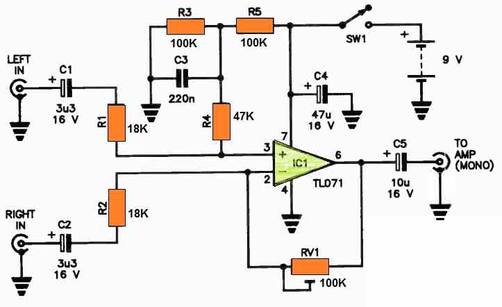
The underlying principle of this circuit relies on the common practice of positioning the vocalist in the center of a stereo recording, where an equal signal is distributed to both audio channels.
By running both channels through this circuit and then routing them back into your amplifier, configured for mono output, you can seamlessly remove the lead vocalist from the audio mix.
To eliminate the need for a split supply rail, a bias voltage equivalent to half of the supply voltage is applied to the non-inverting input of IC1, achieved through the resistor network R3-R5.
The variable resistor RV1 allows you to fine-tune the feedback, enabling you to achieve maximum attenuation of the central stereo signal.
Power can be conveniently sourced from a 9 V transistor radio battery or any other 9 V DC power supply.
Op Amp Phase Splitter Circuit
Suppose you're in the process of designing an audio amplifier circuit and find the need for a phase splitter.
In this scenario, consider employing the following circuit if you have an abundance of IC op-amp packages at your disposal.
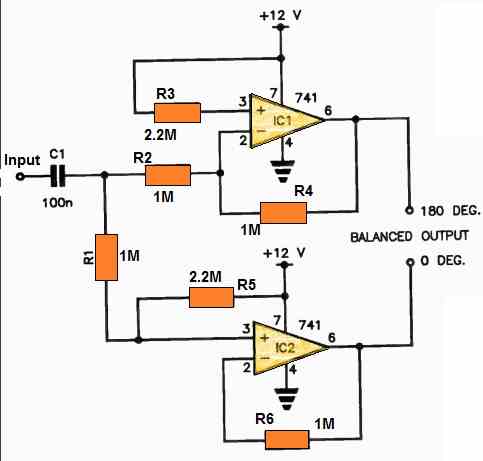
This circuit offers unity gain to both of its outputs and ensures consistent phase splitting across the entire audio frequency spectrum.
You have the flexibility to use either a dual op-amp or two op-amps from a quad package.
Regarding the power supply, it can be selected from any convenient voltage source that falls within the op-amp's specified ratings.
For optimal performance, it's recommended to employ capacitive coupling for the circuit's output.
Darkness Activated Automatic Night Lamp Switch Circuit
Do you wish to activate something when the light diminishes, or perhaps deactivate it? This circuit employs a light-dependent resistor (LDR) to detect variations in light intensity.
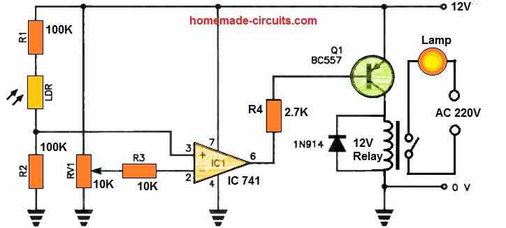
This alteration is magnified through an operational amplifier (op-amp), whose output drives a transistor that controls a relay.
R1 and the LDR constitute one branch of a bridge circuit, while R2 forms the corresponding branch, with RV1 comprising the opposite branches.
The op-amp's differential inputs are connected across the bridge's output. When light shines on the LDR, its resistance decreases.
RV1 is tuned in such a way that the disparity between the inverting and non-inverting op-amp inputs causes the output (pin 6) to go high.
Consequently, there is no base current flowing to Q1, and the relay remains unactivated.
As the light intensity decreases, the resistance of the LDR rises.
This shift in the bridge's output voltage causes the op-amp's non-inverting input (pin 3) to have a lower voltage than its inverting input (pin 2), causing the output to go low. This, in turn, triggers Q1 and activates the relay.
RV1 can be adjusted to ensure that the relay only activates when the light level drops by a predetermined amount, which can be either slight or substantial.
It can be sensitive enough to detect even a slight decrease in light caused by a hand passing in front of the LDR. A 10-turn trimpot is the ideal component to use for RV1.
Wrapping up
So these were a few op amp basic circuits with their parameters explained. Hope you have understood all the characteristics and formulas related to an op amp.
If you have any other basic op amp circuit design that you think needs to be included in the above article, please feel free to mention them through your comments below.


Questions and Answers
Hi dear Mr.Swagatam .
Thank you for your great website. I really learned alot . I designed a simple circuit that has variable output 0 up to 12 volts . The output current is very low about 5mA and i need to boost the current to about 50 mA with the exact same voltage .
I used tda2822m ic but when input voltage is 0 output is 650mv even when i apply dual -5-+5 supply.
What do you suggest?♥️?
Thank you Ehsan,
I checked the datasheet TDA2822 and found that its peak output current is 1 amp. So I am not sure why you are getting 50 mA only.
By input voltage do you mean the audio signal?
Also the input voltage must be around 15V, and this IC does not require dual voltage.
This IC is an audio amplifier IC.
My requiered current is 50 mA.
I just wanted to make the output current stronger and thought that maybe an audio amplifier can do it . What can i do instead?
My input voltage is simple voltage and not a signal . But i can change it from 0 to about 12 v.
I am using a dual 20.-20 volt supply
To make the output current stronger you can use an emitter follower transistor. Take a 2N2222 transistor connect its base with the 0/12V source through a 1k resistor, connect the collector to the +20V, and the load can be connected across emitter of the transistor ad the ground.