• Skip to main content
  • Skip to primary sidebar

Homemade Circuit Projects

Need circuit help? Post them in the comments! I've answered over 50,000!

Blog | Categories | About | Hire Me | Contact | Calculators-online
You are here: Home / Datasheets and Components / IC 4069 Datasheet, Pinout Working, Applications

IC 4069 Datasheet, Pinout Working, Applications

Last Updated on May 17, 2026 by Swagatam 7 Comments

The IC 4069 is a CMOS hex inverter that contains six independent inverter gates. These are called inverters because these gates will always invert the signal at their inputs to produce an opposite signal at their outputs.

Table of Contents
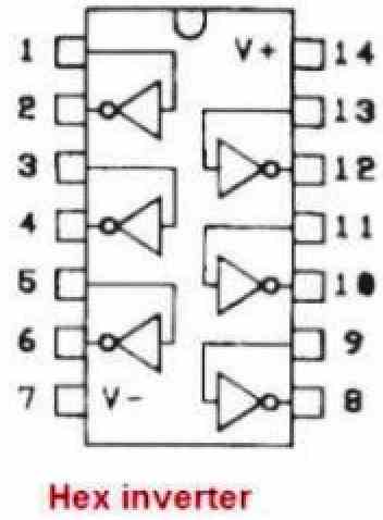
  • Pinout diagram of the IC 4069:
  • Understanding the Pinout Working of the IC 4069
  • Truth Table
  • Features of the IC 4069:
  • Absolute Maximum Ratings
    • DC Electrical Characteristics:
    • AC Electrical Characteristics:
    • Recommended Operating Conditions
    • Application Circuit

Pinout diagram of the IC 4069:

  • Pin 1: Input for inverter 1
  • Pin 2: Output for inverter 1
  • Pin 3: Input for inverter 2
  • Pin 4: Output for inverter 2
  • Pin 5: Input for inverter 3
  • Pin 6: Output for inverter 3
  • Pin 7: Ground or 0V Supply Voltage VSS
  • Pin 8: Output for inverter 4
  • Pin 9: Input for inverter 4
  • Pin 10: Output for inverter 5
  • Pin 11: Input for inverter 5
  • Pin 12: Output for inverter 6
  • Pin 13: Input for inverter 6
  • Pin 14: Positive Supply Voltage VDD

Understanding the Pinout Working of the IC 4069

As explained above, the IC 4069 has six independent NOT gates.

Each of these NOT gates are indicated as 6 individual triangle shaped figures with a small circle at the tip.

Each NOT gate is basically an inverter gate.

Meaning, any signal supplied at the input side of these gates will be instantly inverted and an opposite voltage will be produced at the corresponding output.

Let's take the example of the first gate, with an input at pin#1 and output at pin#2.

When a positive voltage above 2 V but not exceeding the VDD value is applied to its pin#1, then this will be instantly inverted and a 0V will be produced at its pin#2.

Conversely, if a 0V or any voltage below 2 V is applied at pin#1, then again it will be inverted to produce a positive voltage equal to VDD at the output pin#2.

The above functioning is exactly identical for all the six NOT gates of the IC.

Truth Table

The truth table for a single inverter (NOT gate) of the IC 4069 is as follows:

InputOutput
01
10

Because the IC 4069 has six independent inverters, it is possible for us to express its truth table through six columns, where each column represents the truth table for a single inverter.

Input AOutput AInput BOutput BInput COutput C
010101
101010

Each row indicates the input and output for all six inverters of the IC 4069, for a specific combination of inputs.

Features of the IC 4069:

  • Low power consumption
  • Wide operating voltage range (3V to 18V)
  • High noise immunity
  • High speed operation
  • High output current capability

Absolute Maximum Ratings

  • Maximum ratings for supply voltage: 20V
  • Maximum ratings for input voltage: -0.5V to Vdd + 0.5V
  • Maximum ratings for output current: 10mA
  • Maximum ratings for power dissipation: 500mW
  • Maximum junction temperature: 150°C
  • Storage temperature range: -65°C to 150°C

DC Electrical Characteristics:

  • Input voltage high level (VIH): 2V min, 18V max
  • Input voltage low level (VIL): 0V min, 1.3V max
  • Output voltage high level (VOH): 4.5V min, Vdd - 0.1V max (@Vdd = 10V)
  • Output voltage low level (VOL): 0.1V max (@IOL = 4mA, Vdd = 10V)
  • Input leakage current (IIL): -0.1uA to 1uA (@Vdd = 18V, VI = Vdd or GND)
  • Output leakage current (IOZ): -0.1uA to 1uA (@Vdd = 18V, VO = Vdd or GND)
  • Quiescent supply current (IDD): 1uA max (@Vdd = 18V, VI = Vdd or GND)

AC Electrical Characteristics:

  • Propagation delay (tpd): 120ns max (@Vdd = 10V, CL = 50pF)
  • Transition time (tr, tf): 50ns max (@Vdd = 10V, CL = 50pF)

Recommended Operating Conditions

  • Supply voltage range (Vdd): 3V to 18V
  • Input voltage range: 0V to Vdd
  • Operating temperature range: -55°C to 125°C

Application Circuit

The IC 4069 can be used to make a simple light activated switch circuit as shown in the following figure:
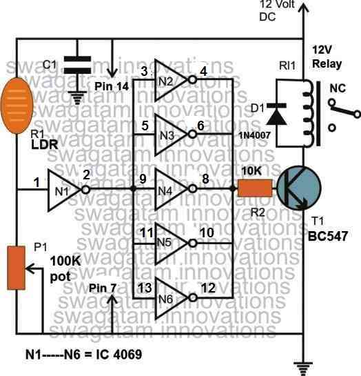
Here, one of the gates of the N1 is configured as a comparator. All the remaining gates N2 to N6 are rigged as buffers and also parallel inverters. This helps to provide sufficient base current for the transistor T1, and also avoids loading of N1.

N1 monitors the potential at its input depending on the adjustment of the P1 and the intensity of the light on the LDR R1.

As long as there is sufficient light, the LDR resistance is low and therefore the input of N1 remains high, causing its output to be low.

The buffer inverters in turn revert this N1 output to a high at their outputs.

This high output activates the transistor and the relay. If a load such as a lamp is connected at the N/C of the relay will be switched OFF in this situation.

When the light intensity decreases, the LDR resistance increases causing a low potential at the input of N1.

Due to this the output of N1 becomes high, causing the outputs of the buffer inverters to become low.

The transistor and the relay are now switched OFF.

Any load such as a lamp connected at the N/C of the relay is now switched ON.
You'll also like:

  • positive feedback hysteresisComparator Datasheet Parameters
  • CreeXlampCree XLamp XM-L LED Datasheet
  • Vibration Sensor 801S Datasheet Explained
  • IC 4043 dtasheet pinoutUnderstanding IC 4043B, IC 4044B CMOS Quad 3-State R/S Latch – Working and Pinouts

Filed Under: Datasheets and Components Tagged With: 4069, Applications, Datasheet, Pinout, Working

About Swagatam

I am an electronics engineer and doing practical hands-on work from more than 15 years now. Building real circuits, testing them and also making PCB layouts by myself. I really love doing all these things like inventing something new, designing electronics and also helping other people like hobby guys who want to make their own cool circuits at home.

And that is the main reason why I started this website homemade-circuits.com, to share different types of circuit ideas..

If you are having any kind of doubt or question related to circuits then just write down your question in the comment box below, I am like always checking, so I guarantee I will reply you for sure!

Previous Post: « IC 4063 Datasheet, Pinout Working, Applications
Next Post: IC 4070 Datasheet, Pinout Working, Truth Table, Electrical Characteristics »

Reader Interactions

Questions & Answers

Total Posts: 7
Newest Oldest
Jedidiah
September 26, 2024 • 2 years ago #161780

Hello Sir.
Can 74LS04 be used as CD4069 substitute?

Reply
SwagatamAdmin
September 27, 2024 • 2 years ago #161837

Hi Jedidiah, yes you can but the maximum supply for the 74LS04 IC cannot be exceeded above 5V.

Reply
Jedidiah
September 27, 2024 • 2 years ago #161871

Thank you Sir.

Reply
Manuel Gavidia
April 13, 2023 • 3 years ago #141772

Hi Swagatam, I need your help. I have a chicago flux 125 that i have problems with the wire feeder control board it uses a CD4069 ic i’m having problems identifying Q2 which is an sot23-3 transistor that pin 3 connects to pin 7 neg- of the 4069 ic and goes on to pins 2 and 1 of the mosfet SVF740T it is an N MOSFET ALSO CAN YOU DETERMINE WHAT ZENER DIODE VALUE IS ZD2? If you can kindly help me figure what that Q2 SOT23-3 and ZD2 is i would greatly appreciate it. I tried contacting the manufacturer but no help it is a discontinued model. iI would like to get it going again. thanks for your help! here is a link to the images i uploaded on facebook Electronics group page. https://www.facebook.com/groups/entspi/posts/9920732267952220/

Reply
SwagatamAdmin
April 14, 2023 • 3 years ago #141786

Hi Manuel,
Sorry, I can’t seem to figure it out….it is very difficult to identify SMD part numbers from a PCB image. If it would be in schematic format then perhaps I could have tried to identify them.

Reply
Doug Adams
March 9, 2023 • 4 years ago #140892

I enjoy your articles, thank you for the effort you exert to create them! I believe that either you mislabeled your schematic, or I am reading it wrong. The pin numbers on the inverters do not match the pinout diagram earlier in the article. For example pin 14 is 12 volts (same as the pinout), but pin 14 is also shown as the input to an inverter in the schematic.

Reply
SwagatamAdmin
March 9, 2023 • 4 years ago #140895

Thank you so much Doug, you are right the circuit diagram had a mistake. Actually the diagram was based on IC 4049 which is exactly similar to 4069 with its functioning.
However, I have now corrected the mistake and changed the pinouts accordingly.
Thank you for pointing out the mistake.

Reply

Need Help? Please Leave a Comment! We value your input—Kindly keep it relevant to the above topic! Cancel reply

Your email address will not be published. Required fields are marked *

Primary Sidebar

My YouTube Channel

Circuit Simulator: Draw and Simulate Schematics

circuit simulator image

Categories

  • Arduino Projects (95)
  • Audio and Amplifier Projects (134)
  • Automation Projects (18)
  • Automobile Electronics (104)
  • Battery Charger Circuits (90)
  • Datasheets and Components (109)
  • Electronics Theory (151)
  • Energy from Magnets and Earth (43)
  • Games and Sports Projects (11)
  • Grid and 3-Phase (20)
  • Health related Projects (27)
  • Home Electrical Circuits (13)
  • Indicator Circuits (16)
  • Inverter Circuits (98)
  • Lamps and Lights (161)
  • Meters and Testers (72)
  • Mini Projects (28)
  • Motor Controller (68)
  • Oscillator Circuits (30)
  • Pets and Pests (15)
  • Power Supply Circuits (91)
  • Remote Control Circuits (50)
  • Security and Alarm (65)
  • Sensors and Detectors (107)
  • SMPS and Converters (46)
  • Solar Controller Circuits (62)
  • Temperature Controllers (44)
  • Timer and Delay Relay (51)
  • Voltage Control and Protection (44)
  • Water Controller (37)
  • Wireless Circuits (31)

Subscribe to get New Circuits in your Email

Other Links

  • Privacy Policy
  • Cookie Policy
  • Disclaimer
  • Copyright
  • Videos
  • Sitemap

People also Search

555 Circuits | 741 Circuits | LM324 Circuits | LM338 Circuits | 4017 Circuits | Ultrasonic Projects | SMPS Projects | Christmas Projects | MOSFETs | Radio Circuits | Laser Circuits | PIR Projects |

Recent Comments

  • Michael on Electronic Circuit Projects, Tutorials, and Practical Engineering Solutions
  • Swagatam on 24V to 12V DC Converter Circuit [using Switching Regulator]
  • Swagatam on Automatic Battery Full Cut-Off Latching Circuit with Trickle Charging
  • Ramin on Automatic Battery Full Cut-Off Latching Circuit with Trickle Charging
  • Joss on 24V to 12V DC Converter Circuit [using Switching Regulator]

Social Profiles

  • Twitter
  • YouTube
  • Instagram
  • Pinterest
  • My Facebook-Page
  • Stack Exchange
  • Linkedin

Calculators

  • ZVS Induction Heater + Tank Calculator Tool
  • Zener Diode Calculator
  • Wire Current and Thickness Calculator (Ampacity Calculator)
  • Voltage Divider Calculator
  • Transistor Base Resistor Calculator
  • Transistor Astable Multivibrator Calculator
  • TL431 Calculator
  • Solar Panel, Inverter, Battery Calculator
  • Ferrite Core Air Gap Calculator Tool
  • Parallel MOSFET Calculator Tool: How to Connect MOSFETs in Parallel Safely
  • LC Resonance Calculator for EV Battery Charger Circuits
  • LED String Series Resistor Calculator
  • PFC (Power Factor Correction) Calculator Tool: 3kW
  • Passive Power Factor Correction (PFC) Calculator
  • LM567 IC Calculator Tool
  • SMPS Flyback Boost Converter Calculator
  • Shunt Resistor Calculator for Ammeters
  • SCR and Triac Gate Resistor Calculator
  • Battery Back up Time Calculator
  • Boost Converter Calculator (Non-Isolated)
  • Bootstrap Capacitor Calculator
  • Buck Converter Calculator
  • Buck-Boost Converter Calculator
  • Capacitance Reactance Calculator
  • DCM Flyback Transformer & Wire Gauge Wire Size Calculator Tool
  • Filter Capacitor Calculator
  • IC 4047 Calculator (Frequency and PWM)
  • IC 4060 Calculator
  • IC 555 Astable Calculator
  • IC 555 Monostable Calculator
  • IC SG3525, SG3524 Calculator
  • Inductance Calculator
  • Induction Heater Inductor and Resonant Frequency Calculator
  • Induction Heater Work Coil Calculator
  • Inverter LC Filter Calculator
  • LC Resonance Calculator
  • LED Current Calculator
  • LM317, LM338, LM396 Calculator
  • NAND/NOT Gate RC Values Calculator
  • NOT, NAND Gate Frequency Calculator
  • Notch Filter Calculator Tool
  • Ohm’s Law Calculator
  • Phase Angle Phase Shift Calculator
  • Power Factor (PF) Calculator
  • RC Filter Calculator
  • Reactance Calculator
  • Sine Table Calculator for SPWM Arduino Code
  • Small Signal Transistor(BJT) and Diode Quick Datasheet
  • SMPS Calculator for Toroidal Ferrite Transformers
  • SMPS Flyback Transformer Calculator – Design by Target Duty Cycle
  • TL431 Calculator
  • Op-Amp Hysteresis Resistor Calculator

© 2026 · Swagatam Innovations