This post will help you to understand a few of the crucial comparator parameters or specifications which are generally found in comparator IC datasheets.
Some of the major parameters that you may come across in the datasheet of a compartaor are:
- Propagation delay
- Current consumption
- Output stage type (open collector/drain or push-pull)
- Input offset voltage, hysteresis
- Output current capability
- Rise and fall time
- Input common mode voltage range
Apart from these you may also find other parameters such as: input bias current, common mode and power supply rejection ratio, sample/hold function, and startup time.
Mostly, a single comparator chip will have 5 pins: a couple of pins for power input VCC+,VCC-, two pins for feeding the input signals IN+, IN- and a single output OUT pin. In some ICs there may be an extra pin for the standby function.
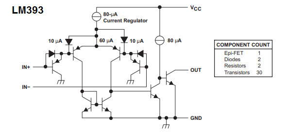
From our earlier discussions we know that when VIN(+) > VIN(-), the output is in high state, if VIN(+) < VIN(-), the output is in low state.
In other words when the non-inverting input (+) has a higher level of voltage than the inverting input (-), the output transistor inside the compartaor will be switched OFF.
Meaning its collector pin will show an open condition. Since this collector pin is supposed to be linked with the positive supply rail through a pull-up resistor, allows the collector to have a positive or a high logic output in this situation.
Output stage type (open collector/drain or push-pull)
With regards to the output pin configuration, comparators are of two types: push-pull and open collector (open drain).
In a push-pull configuration, the load may be directly connected between the collector pin of the compartaor and the positive line which allows the load to be switched ON/OFF depending on the input signal conditions. This works like a push-pull switching and hence the name.
Alternatively the collector pin can be connected with the positive rail through a pull-up resistor, and then the collector output may be used as a push-pull logic output. One os the advantages of this configuration is it enables a different voltage level than the Vcc of the comparator to be used for the load.
In the open collector mode, the comparator can only sink current, but cannot supply current to the load. Due to its limited scope this mode is rarely used, although it allows more than one output to be connected in the OR gate mode for a specified application.
Comparator Datasheet Parameters
Input common mode voltage range - VICM :
Input common mode voltage range is a measure of voltage which comes within the acceptable input range of the compartaor.
It's a voltage range in which both the inputs of the compartaor are mandatorily used for ensuring the functioning of the configuration.
In this mode the inputs work with the complete Vcc to 0V supply range across their input pins, hence it's also called rail to rail input stage.
However, it is recommended to avoid a rail to rail common mode input range unless it's necessary, to minimize power consumption of the device.
Input offset voltage - VIO (VTRIP)
The VIO parameter is the minimum input difference value which may be at the verge of causing the output to toggle its state. Input offset voltage differential level at the input can affect the resolution of the comparator because this differential magnitude could be very small and cause instability for the output toggling state. Therefore such small offset signals may cause the output to behave abnormally or simply not switch at all.
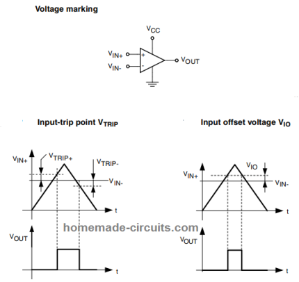
Low differential may cause the comparator transistor to become unstable resulting in an increase in the input offset voltage conditions to increase.
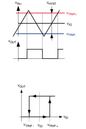
For compartaor that have internal hysteresis enabled VIO is defined as the average level of the sum of of VTRIP+ and VTRIP-, and the hysteresis value of VHYST = VTRIP+ - VTRIP- where VTRIP+ and VTRIP- constitute the input differential voltage that causes the output to switch from low to high state or high to low state respectively.
CMRR and SVR
CMRR stands for common mode voltage rejection ratio, provides the relationship between input offset voltage VIO and the input common mode voltage VICM. This may be understood as a ratio of common mode voltage value upon the input offset voltage. This parameter is usually expressed in logarithmic scale as:
CMRR [dB] = 20 • log (| ΔVICM /ΔVIO| )
CMRR is calculated by measuring two input offset voltage magnitudes taken for two different input common mode voltages (typically 0 V and VCC).
The term SVR stands for “supply voltage rejection” and is defined as a parameter that provides the relation between the input offset voltage VIO and the power supply voltage.
Changing power supply voltage has the ability to somewhat affect the bias of the input differential transistor pairs. This implies that the variation might also cause the input offset voltage to change slightly.
This is expressed through the formula:
SVR [dB] = 20 • log (| ΔVCC /ΔVIO| )
Voltage gain
This parameter helps us to understand the net gain of the comparator. When the comparator is attributed with higher gain specs, it means an improved response of the device to small input signal differentials.
Typically the AVD range of a compartaor can be 200V/mV(106dB). Theoretically, amplitude of 200V is achieved when a 1mV input is amplified with 106dB. However, for a real device the peak level swing will be limited by the value of Vcc.
Note that the AVD can never have any effect on external hysteresis since the output will be either in high or low state, and never in between .
Propagation delay
TPD is defined as the time difference between the instant when the input signal just crosses the reference input level and the instant when the output state has just changed states.
From our previous discussions we know that the output of the compartaor toggles in response to input pin voltage difference.
Propagation delay TPD provides us with the specification that suggest how quickly the input pins have the ability to sense the difference and toggle the output without problems.
Basically, TPD tells us about the input frequency level which the comparator can process comfortably for generating valid output responses.
Hysteresis
We know that hysteresis is a parameter that prohibits quick changes of an output in response to an unstable or fluctuating input.
Normally, in a comparator the output voltage can oscillate or fluctuate rapidly when the input differential signal hovers close to the reference value. Or this may happen when the input signal has a very low amplitude, causing the input differential level to change at a quick rate.
Built-in hysteresis
There are actually many comparator devices that feature a built in hysteresis functionality. This may be around at a few mV, which is quite enough to suppress undesired output switching without affecting the devices resolution.
For such devices, the evaluated average upper and lower voltage limits is called input offset voltage VIO, and the difference VTRIP+/VTRIP- is termed as hysteresis voltage or VHYST.
External Hysteresis
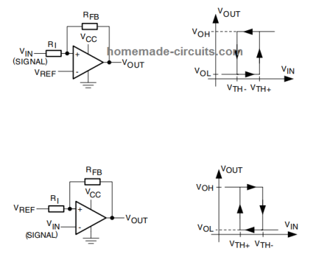
In case the comparator is without an in-built hysteresis, or if the intended hysteresis level is relatively bigger, then an external configuration may be added for implementing the hysteresis functionality via a positive feedback network, as shown below.
Wrapping up
So these a few crucial compartaor datasheet parameters which will be helpful for all enthusiast trying to achieve a prefect comparator based design, if you have further information regarding this subject please feel free to share them through your comments.

Need Help? Please Leave a Comment! We value your input—Kindly keep it relevant to the above topic!