The IC 4069 is a CMOS hex inverter that contains six independent inverter gates. These are called inverters because these gates will always invert the signal at their inputs to produce an opposite signal at their outputs.
Pinout diagram of the IC 4069:
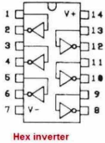
- Pin 1: Input for inverter 1
- Pin 2: Output for inverter 1
- Pin 3: Input for inverter 2
- Pin 4: Output for inverter 2
- Pin 5: Input for inverter 3
- Pin 6: Output for inverter 3
- Pin 7: Ground or 0V Supply Voltage VSS
- Pin 8: Output for inverter 4
- Pin 9: Input for inverter 4
- Pin 10: Output for inverter 5
- Pin 11: Input for inverter 5
- Pin 12: Output for inverter 6
- Pin 13: Input for inverter 6
- Pin 14: Positive Supply Voltage VDD
Understanding the Pinout Working of the IC 4069
As explained above, the IC 4069 has six independent NOT gates.
Each of these NOT gates are indicated as 6 individual triangle shaped figures with a small circle at the tip.
Each NOT gate is basically an inverter gate.
Meaning, any signal supplied at the input side of these gates will be instantly inverted and an opposite voltage will be produced at the corresponding output.
Let's take the example of the first gate, with an input at pin#1 and output at pin#2.
When a positive voltage above 2 V but not exceeding the VDD value is applied to its pin#1, then this will be instantly inverted and a 0V will be produced at its pin#2.
Conversely, if a 0V or any voltage below 2 V is applied at pin#1, then again it will be inverted to produce a positive voltage equal to VDD at the output pin#2.
The above functioning is exactly identical for all the six NOT gates of the IC.
Truth Table
The truth table for a single inverter (NOT gate) of the IC 4069 is as follows:
| Input | Output |
|---|---|
| 0 | 1 |
| 1 | 0 |
Because the IC 4069 has six independent inverters, it is possible for us to express its truth table through six columns, where each column represents the truth table for a single inverter.
| Input A | Output A | Input B | Output B | Input C | Output C |
|---|---|---|---|---|---|
| 0 | 1 | 0 | 1 | 0 | 1 |
| 1 | 0 | 1 | 0 | 1 | 0 |
Each row indicates the input and output for all six inverters of the IC 4069, for a specific combination of inputs.
Features of the IC 4069:
- Low power consumption
- Wide operating voltage range (3V to 18V)
- High noise immunity
- High speed operation
- High output current capability
Absolute Maximum Ratings
- Maximum ratings for supply voltage: 20V
- Maximum ratings for input voltage: -0.5V to Vdd + 0.5V
- Maximum ratings for output current: 10mA
- Maximum ratings for power dissipation: 500mW
- Maximum junction temperature: 150°C
- Storage temperature range: -65°C to 150°C
DC Electrical Characteristics:
- Input voltage high level (VIH): 2V min, 18V max
- Input voltage low level (VIL): 0V min, 1.3V max
- Output voltage high level (VOH): 4.5V min, Vdd - 0.1V max (@Vdd = 10V)
- Output voltage low level (VOL): 0.1V max (@IOL = 4mA, Vdd = 10V)
- Input leakage current (IIL): -0.1uA to 1uA (@Vdd = 18V, VI = Vdd or GND)
- Output leakage current (IOZ): -0.1uA to 1uA (@Vdd = 18V, VO = Vdd or GND)
- Quiescent supply current (IDD): 1uA max (@Vdd = 18V, VI = Vdd or GND)
AC Electrical Characteristics:
- Propagation delay (tpd): 120ns max (@Vdd = 10V, CL = 50pF)
- Transition time (tr, tf): 50ns max (@Vdd = 10V, CL = 50pF)
Recommended Operating Conditions
- Supply voltage range (Vdd): 3V to 18V
- Input voltage range: 0V to Vdd
- Operating temperature range: -55°C to 125°C
Application Circuit
The IC 4069 can be used to make a simple light activated switch circuit as shown in the following figure:
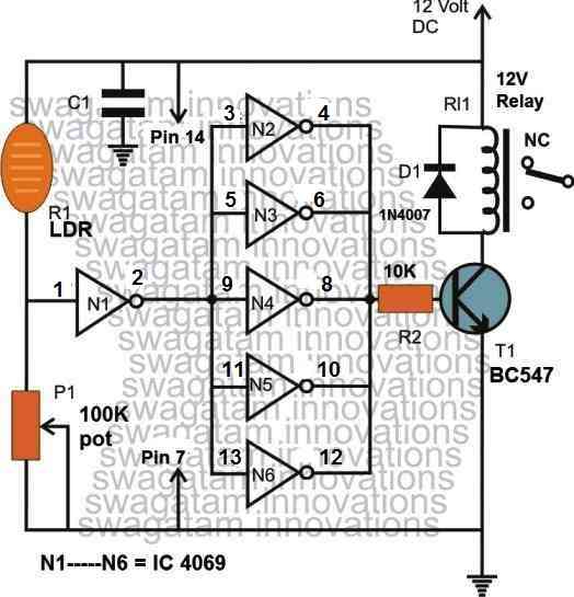
Here, one of the gates of the N1 is configured as a comparator. All the remaining gates N2 to N6 are rigged as buffers and also parallel inverters. This helps to provide sufficient base current for the transistor T1, and also avoids loading of N1.
N1 monitors the potential at its input depending on the adjustment of the P1 and the intensity of the light on the LDR R1.
As long as there is sufficient light, the LDR resistance is low and therefore the input of N1 remains high, causing its output to be low.
The buffer inverters in turn revert this N1 output to a high at their outputs.
This high output activates the transistor and the relay. If a load such as a lamp is connected at the N/C of the relay will be switched OFF in this situation.
When the light intensity decreases, the LDR resistance increases causing a low potential at the input of N1.
Due to this the output of N1 becomes high, causing the outputs of the buffer inverters to become low.
The transistor and the relay are now switched OFF.
Any load such as a lamp connected at the N/C of the relay is now switched ON.


Comments (7)
Hello Sir.
Can 74LS04 be used as CD4069 substitute?
Hi Jedidiah, yes you can but the maximum supply for the 74LS04 IC cannot be exceeded above 5V.
Thank you Sir.
Hi Swagatam, I need your help. I have a chicago flux 125 that i have problems with the wire feeder control board it uses a CD4069 ic i’m having problems identifying Q2 which is an sot23-3 transistor that pin 3 connects to pin 7 neg- of the 4069 ic and goes on to pins 2 and 1 of the mosfet SVF740T it is an N MOSFET ALSO CAN YOU DETERMINE WHAT ZENER DIODE VALUE IS ZD2? If you can kindly help me figure what that Q2 SOT23-3 and ZD2 is i would greatly appreciate it. I tried contacting the manufacturer but no help it is a discontinued model. iI would like to get it going again. thanks for your help! here is a link to the images i uploaded on facebook Electronics group page. https://www.facebook.com/groups/entspi/posts/9920732267952220/
Hi Manuel,
Sorry, I can’t seem to figure it out….it is very difficult to identify SMD part numbers from a PCB image. If it would be in schematic format then perhaps I could have tried to identify them.
I enjoy your articles, thank you for the effort you exert to create them! I believe that either you mislabeled your schematic, or I am reading it wrong. The pin numbers on the inverters do not match the pinout diagram earlier in the article. For example pin 14 is 12 volts (same as the pinout), but pin 14 is also shown as the input to an inverter in the schematic.
Thank you so much Doug, you are right the circuit diagram had a mistake. Actually the diagram was based on IC 4049 which is exactly similar to 4069 with its functioning.
However, I have now corrected the mistake and changed the pinouts accordingly.
Thank you for pointing out the mistake.