The following article which discusses a 300 watt pure sine wave inverter circuit with automatic output voltage correction, is a modified version of one of my previous posts, and was submitted to me by Mr. Marcelin. I have explained more about the converter implementations.
The Design
The idea was inspired by the design presented in this article by me, however Mr.Marcelin has refined it considerably for better efficiency and reliability.
To me, the modifications and the implementations done look great and feasible.
So I have explained the design elaborately with the following points:
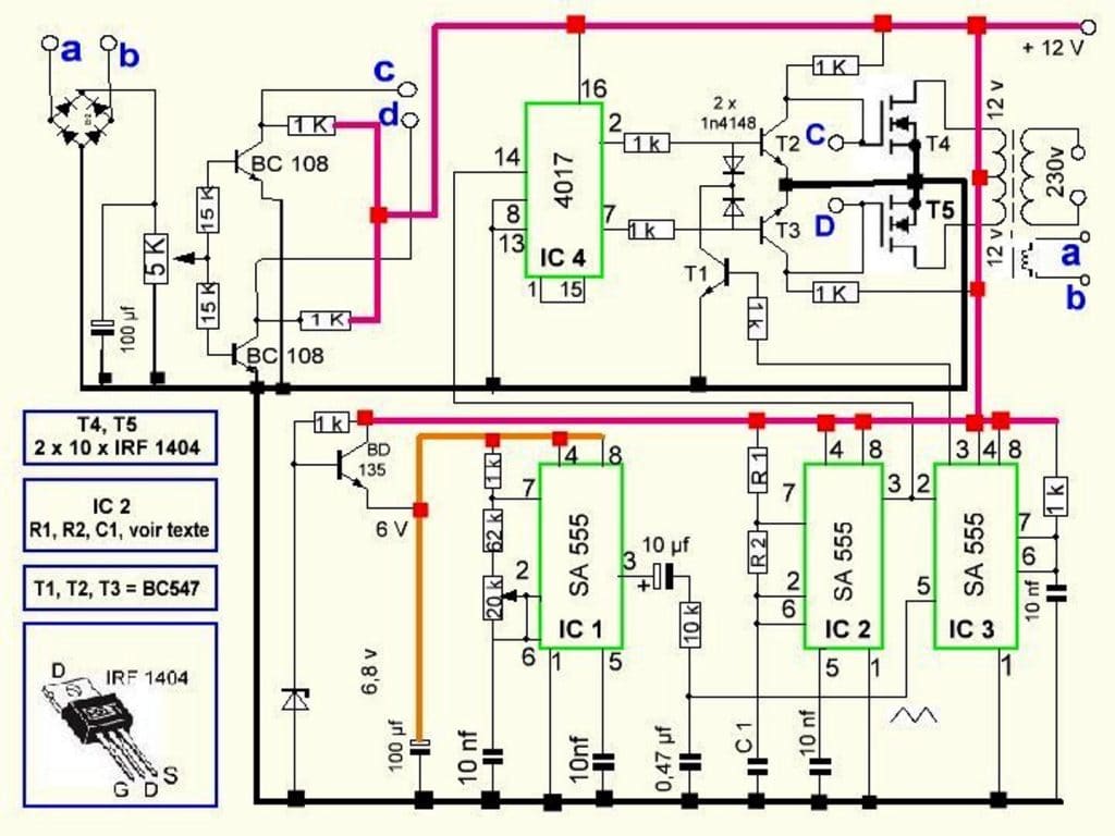
IC2 and IC3 are specifically configured as the PWM generator stage.
IC2 forms the high frequency generator required for pulsing the PWM waveform which is processed by IC3.
For processing the IC2 pulses, IC3 needs to be fed with a sine wave equivalent information at its pin#5, or the control input.
Since creating sine waveform is a bit complex than a triangular waves, the later was preferred as its easier to make yet performs as good as a sine waveform counterpart.
IC1 is wired up as the triangular wave generator, whose output is finally fed to pin#5 of IC3 for the generating the required RMS sine equivalent at its pin#3.
However the above processed PWM signals needs to be modulated over a push-pull kind of arrangement so that the waveforms are able to load the transformer with alternately conducting current.
This is necessary for achieving an output mains consisting of both positive and the negative half cycles.
Circuit Operation
The IC 4017 is introduced just for implementing this action.
The IC generates a sequentially running output from its pin#2 to pin#4, to pin #7, to pin#3 and back again to pin#2, in response to every rising pulse edge at pin #14.
This pulse is derived from the output of IC2, which is set to 200 Hz strictly so that the outputs of IC4017 results in a 50 Hz across the sequencing from the above discussed pin outs.
Pin#4 and pin#3 are purposely skipped, for generating a dead time across the gates triggers of the respective transistors/mosfets connected to the relevant outputs of IC4017.
This dead time makes sure that the devices never conduct together even for a nano second at transition zones, and thus safeguard the health of the devices.
The sequencing positive outputs at pin#2 and 7 trigger the respective devices which in turn force the transformer to saturate with the alternating battery power induced in the respective winding.
This results in the generation of around 330+ V AC at the output of the transformer.
However this voltage would be a square wave with high RMS if it wouldn't be processed with the PWM from IC3.
Transistor T1 along with its collector diode is fed with the PWM pulses such that T1 now conducts and grounds the base trigger voltages of the outputs devices in accordance with the PWM content.
This results in an output that's an exact replica of the the fed PWM optimized input..... creating a perfectly carved pure sine wave AC equivalent.
The circuit has additional features such as a manual output voltage correction circuit.
The two BC108 transistors are stationed for controlling the gate drive voltage levels of the mosfets, the base current of these transistors are derived from a small sensing winding on the transformer which provides the required output voltage level information to the transistors.
If the output voltage goes beyond the expected safe level, the base current of the above transistors may be adjusted and reduced by varying the 5K preset, this in turn brings down the conduction of the mosfets, ultimately correcting the output AC to the required limits.
The BD135 transistor along with its base zener provides a stabilized voltage to the associated electronics for sustaining constant PWM output from the relevant ICs.
With IRF1404 as the mosfets, the inverter would be able to generate anywher around 300 to 5000 watts of pure sine wave output.
Many drawbacks and flaws were detected while assessing the above circuit details. The finalized circuit (hopefully) is presented below.
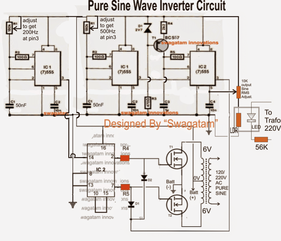
The above circuit may be further enhanced with an automatic load correction feature as shown below. It is implemented by the inclusion of the LED/LDR opto-coupler stage.
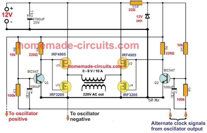
For the final verified design of the above circuit please refer to the following post:https://www.homemade-circuits.com/2013/10/modified-sine-wave-inverter-circuit.html



Questions & Answers
yes you can use irf240. first test with single mosftes, if it works then proceed with more nos.
you can try the last circuit given in the following article:
https://www.homemade-circuits.com/2012/12/make-this-ic-556-pure-sine-wave.html
Thanks Michael, I referred you to the new circuit since you had asked for a simplified and a reliable diagram, you can continue with the above diagram if you feel so, no issues.
The 556 will not require any regulation as it can work with any voltage from 5 to 15V and will produce the same results.
By the way the new diagram is RMS controlled and would hopefully produce a constant voltage with varying load conditions.
Also please note that none of these designs have been practically confirmed by me, they are all produced using mind simulation.
…deriving voltage directly from 220v tap would be posible using a 0.22/400v capacitor for dropping the current and then rectified for feeding the shown transistor stage.
Which 555 circuit are you referring to? the above one or the linked one.
the linked one will not require an external triangle wave generator, it has a built in.
use the following circuit across points a/b.
https://www.homemade-circuits.com/2011/12/cheap-yet-useful-transformerless-power.html
use a 0.22uF capacitor for C1 and don't use the zener diode.
the 5k preset now should be replaced with a 47K preset.
The voltage will get adjusted by the 5k preset, there's no need of adding 7806 IC, if you add it then the detection might not take place.
you can use 9-0-9v/25amp transformer.
7805 will not be required with 12v supply
I have worked hard to present the concept, and I will request you to simulate it or test it practically so that all others can benefit from it.
I wish you all the best for the project.
When two waves are fed to an opamp inputs the internal circuitry compares the two voltage peaks and produce the average waveform of the two through varying rectangular waveform and duty cycle. Since the output from the opamp can be either low or high therefore the result is always in the form of rectangular wave and cannot be exponential.
4017 will not respond to PWM, it will only follow the high peaks and make it's output jump from one output to the next, it won't reproduce the PWMs.
During the PWM high pulses the transistor conducts and grounds the equivalent amount of areas from the mosfet base square waves allowing the mosfet to conduct exactly according to the PWM pattern.
That's exactly why the diodes are there. The diodes prevent positive PWMs from entering the N-channel mosfet gates making sure their gate conduction is chopped only through the negative PWMs which would otherwise have no effect on the mosfet conduction.
Thank you Michael, interesting questions, I think all these can be easily confirmed through practical testes, because doing mind simulations could possibly produce wrong results.
So the best thing to do is take an opamp, feed the proposed signals at the inputs and analyze the readings at the the output over an oscilloscope.
I appreciate your interesting thoughts, keep them coming:)
Refer to this circuit, here the low amplitude signals are appropriately amplified at the output for driving the inverter transformer:
https://www.homemade-circuits.com/2013/04/simple-pure-sine-wave-inverter-circuit.html
Hi Bro, you are such a genius in this things, now can you give us a PCB for this to enable easy building of the project
Thank you Darlington, However I am sorry to say that it won't be feasible for me to design the PCB due to my busy schedule, yet I'll see if I can do it some time in the future.
The 1K will block this from happening to appreciable limits, only a trivial amount will pass and get grounded inside the pins and will have no affect on the functioning.
I am sorry Michael, It's difficult to figure out just by visualizing, you will have to check it in scope.
The -12V is actually the 0V line or the ground line, a single battery is used for the design.
Higher resistance will prevent quick discharge of mosfets internal capacitance making it inefficient.
You are welcome Michael, your questions are always interesting.
A wattage selector is not required actually, because the inverer does this automatically…..when more load is connected the output starts drawing more current from the battery and vice versa, just like our home electrical system, with more load we are billed more and so on.
You will need battery charger unit which you can wire with the relay changeover system shown in the following link:
https://www.homemade-circuits.com/2012/09/automatic-inverter-supply-and-mains.html
It will charge your battery when mains is present and revert the battery to inverter mode when AC fails, also the output to the appliances will be switched from mains to inverter and vice versa.
ACTUALLY THE BC108 SECTION IS INCORRECT, I noticed it carefully just now. The situation will not allow the mosfets to conduct at all.
The BC108 must be replaced with PNP transistors such as BC557 which will then work as "emitter followers" and restrict the mosfet voltage exactly to the level which is set at their bases.
To know more regarding the above just Google, "how emitter follower transistor work"
the situation here will be just the opposite to BC108s, for BC557 the emitters will go to the mosfet gates, collector as mentioned by you will go to the ground.
emitters will not need any resistors because of the 1k resistors from the IC 4017 relevant pinouts.
you are welcome Michael!
Everything is correct in your explanation.
The carrier waves decide the frequency of the PWM so it has nothing to do with filtration at the output, the output will be a clean PWM in sync with the sine generated by the "bubba"
The above diagram may have a few discrepancies, please refer to the LAST diagram given in the following link, it's at par with your explanation except that it doesn't employ a sine oscillator:
https://www.homemade-circuits.com/2012/12/make-this-ic-556-pure-sine-wave.html
Dear Raimund,
The above circuit was designed by one of the interested hobbyists, so it might have some issues with its configuration, you can refer to the last design presented in the following link:
https://www.homemade-circuits.com/2012/12/make-this-ic-556-pure-sine-wave.html
It's simple and as good as the above explained circuits.
Actually there's nothing called carrier waves here, one signal determines the frequency of the PWM while the other the duty cycle, together they constitute and produce the required optimized PWM corresponding to the applied sine input.
for example when you apply the two signals at the inputs of an opamp, the output results in a PWM where the ramp (sine or triangle waves) voltage fixes the pulse width while the square waves determines the frequency of the pulses
you may incude for better safety, although nowadays the mosfets have them in-built.
I think you've made a good point, the transistor is not required, in-fact it's presence will invert the PWM from the 555 output, resulting in an incorrect stepped-down voltage at the tranfo output.
the common cathodes of the diodes must be directly connected with the 555 output for obtaining correct optimization.
1) That's correct, however the triangle waveform is not critical, it can be replaced with square waves at pin#2.
2) just divide the number of sequence selected for the output of 4017 and multiply it with 50, that will give you the IC1 frequency value, which can be set by adjusting C1.
3)It may be connected in that way, but having separate resistors for the gates would be better.
correction:
2)just multiply the number of sequence selected for the output of 4017 with 50, that will give you the needed IC1 frequency value, which can be set by adjusting C1
Hi Michael, you are right! Actually I have already addressed this issue to one of the readers who asked the same question a few days back, I can't remember though where it's posted.
Anyway the remedy may be done in the following manner.
another resistor can be introduced in between the IC pinouts and the common gate resistors, and this junction can be used as the PWM and the voltage correction outputs.
The new resistor can be a 1K while the gate resistors can be reduced to 100 ohms.
hello Sir….
what if i increase the frequency of the output pwm IC??(IC3 in first diagram)…
the output frequency would also increase then.
Thanks Michael,
The resistors are introduced neither for limiting current nor for restricting voltage, it's just a good practice to put a low value resistor at the gate….even if you don't put any resistor the mosfets won't get affected because these are MOS based devices specified with very high gate resistance.
Applying the PWM at the IC pins would blow the 4017 IC.
in cases where there's no return path for the mosfet gate to discharge then it would be required.
it can used to control the height ( peak voltage) of the triangle waves resulting in an equivalent control at the output
Actually the above modification won't correct a varying output load, so yes may be the modification was not correct, I'll redesign it and publish it soon.
the present design would reduce the positive PWMs which we don't want, it should be just the opposite, so you are right the modification should be introduced at the gates of the mosfets, I'll correct it accordingly soon.
The "space" in the mark/space ratio of PWMs are the negative pulses, wider "spaces" would result in lesser voltage while wider "marks" would result in increasing voltages.
I have updated the required design, you can check it out.
I did not modify the first design because it's unnecessarily complicated, rather I designed my own version, see the last diagram.
Here I have eliminated the triangle waves because according to me the pattern of the waveform is not critical, the RMS needs to be corrected as per the specifications which I have tried to do through the opto circuit.
The shown optocoupler is a hand made assembly made by sealing an LDR and LED face-to-face inside a light proof enclosure.
I have already rejected the first diagram due to many doubtful things hidden in it, so it's no use sending me the diagram.
First of all the triangle waves shown there may not be from zero to peak, secondly the voltage correction stage is doubtful..
The updated diagrams at the bottom are more reasonable and are on the same principles as the first one, except that it does not employ triangle waves which is anyway not crucial, according to me.
The varying voltage level of the triangle waves determine the output pulse width therefore if the triangle waves are without sufficient peak levels, the result from pin#3 would be proportionately low which in turn will produce lower AC voltage at the output of the trafo.
In the modified diagram I have eliminated the triangle waves because here I have empoyed a fixed average voltage at pin#5 such that the corresponding average PWM matches with the average of a triangle wave.
You can refer to the following post for knowing more about 555 function as a pwm generator.
https://www.homemade-circuits.com/2012/12/how-to-use-ic-555-for-generating-pwm.html
Technically it should be equal to the transformer half winding voltage rating, that is if the trafo is 9-0-9V, then you may fix a 9V DC at pin#5 of IC2 for getting the specified output at the trafo output
with 12V trafo if the mosfets are allowed to push 12V into the trafo then the output would be equal to the rated output voltage.
Using PWM we can reduce the average conduction of the mosfets thereby reducing their average ON time which in turn produces proportionately lower output voltage at the output of the trafo
that's correct.
Yes a lower voltage trafo will generate a slightly higher voltage at the output and thus will last longer even when the battery is fully discharged.
If you are using a 12V battery then you can directly connect it with the ICs.
The meter is showing the RMS value or the average value, the peak voltage of the pulses are always 12V or equal to the supply voltage, so the mosets would be conducting fully during those instantaneous peak pulses.