If you want to build a very heavy power inverter or when you want to make a high frequency induction heater, or when you want to make a lab grade variable SMPS, then getting precise control over both output voltage and current is a major engineering hurdle. Most standard designs using the classic SG3525 PWM controller rely heavily on its internal error amplifier. But this internal amplifier is very bad when you try to implement dual loop Constant Voltage / Constant Current (CV/CC) adjustments.
If you attempt to connect both a voltage adjustment potentiometer and a current limiting potentiometer to the same internal pin of the SG3525, then the loops will aggressively fight each other. This results in severe control conflicts, voltage sagging under heavy loads, and dangerous hunting or oscillation behaviors.
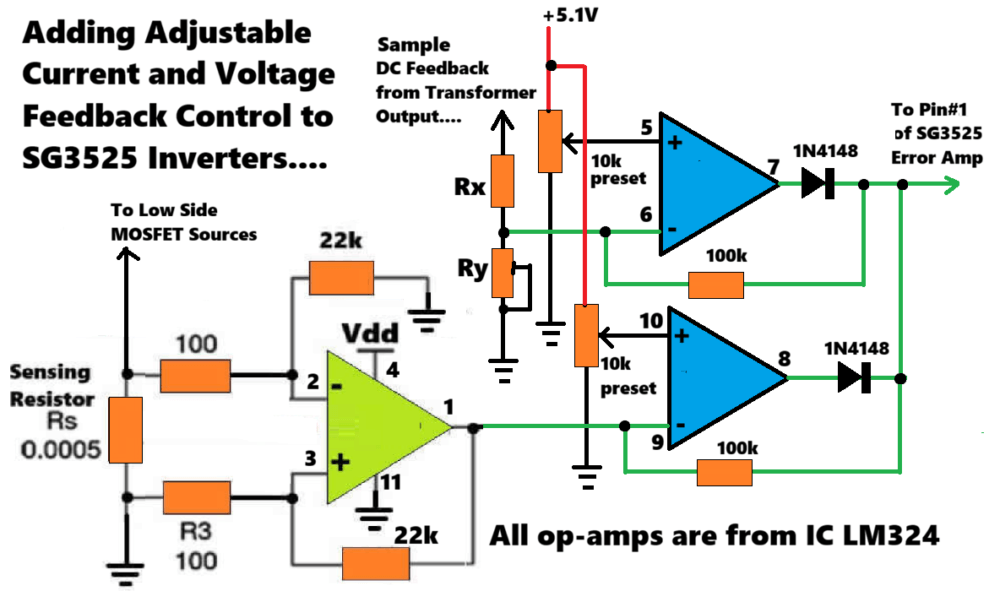
Since this is a big problem, so now, in this super simple guide, we break down a bulletproof bench tested analog auctioneering circuit using a single LM324 Quad Operational Amplifier. This topology cleanly isolates your tracking loops, introduces active heat drift compensation and hands over a mathematically unified control signal straight to Pin 1 of the SG3525.
WHY STANDARD DESIGNS FAIL
In a variable lab bench power supply, when the load demands power then the circuit must operate in two different profiles based on that demand:
- Constant Voltage (CV) Mode: The voltage stays locked precisely at your user defined target, for example 12V, while the current fluctuates naturally based on what the load pulls.
- Constant Current (CC) Mode: If the load tries to draw more current than your safe preset threshold, then the power supply must instantly suppress its voltage output, dropping it as low as necessary to clamp the current precisely at that limit.
To transition between these two states without any manual switching, let us create an analog auction block. The ideal way to build this is a highest voltage wins diode OR network. When your tracking loop senses that its parameter has crossed the user defined target then it will output a high voltage signal.
This signal rides through an isolation diode, commands Pin 1 of the SG3525, and pinches down the PWM duty cycle.
But silicon diodes introduce a flat 0.6V forward voltage drop (V_F) that shifts dynamically with ambient temperature. If left uncompensated, then your power supply output voltage will drift significantly as the enclosure warms up.
The schematic below elegantly solves this because it embeds the diodes directly into the active feedback paths of the op amps.
COMPREHENSIVE CIRCUIT ANALYSIS
The complete control block is implemented using three out of the four independent operational amplifiers available inside a single LM324 Quad Op Amp IC. This layout keeps your PCB footprint highly compact since all three stages share a single, stable housekeeping power rail with V_dd on Pin 4 and GND on Pin 11.
- The High Precision Shunt Amplifier (Green Stage) Reading current accurately on a high power ground rail without picking up stray switching noise requires a robust differential configuration.
A low value 0.0005 Ohm current sensing shunt resistor (R_s) is placed directly in the main ground return line of the low side MOSFET sources.
When a massive 10A continuous load flows then this shunt drops a minute 5 mV (10A * 0.0005 Ohm = 0.005V), keeping power dissipation exceptionally low and preventing thermal resistance drift.
- Pin 2 (Inverting Input -): Connects to the top hot side of the shunt resistor through an isolation 100 Ohm resistor.
- Pin 3 (Non Inverting Input +): Connects to the absolute system ground side of the shunt through an identical 100 Ohm balancing resistor (R_3).
- Pin 1 (Output): To magnify the tiny 5 mV signal into a usable analog voltage range, a 22k resistor is placed across Pin 1 and Pin 2.
This sets a precise differential gain of 220 (22k / 100 = 220). Consequently, when your circuit draws 1A, then Pin 1 outputs 0.11V. When it draws a full 10A, then Pin 1 scales linearly to exactly 1.10V.
- The Active Voltage Regulation Loop (Top Blue Stage) The top amplifier operates as the Constant Voltage error generator. It compares your desired output target against the real time scaled output of the inverter or SMPS.
- Pin 5 (Non Inverting Input +): Connects directly to the center sliding wiper of a 10k Voltage Adjustment Potentiometer. This potentiometer is slung across the ultra stable +5.1V reference rail provided directly by Pin 16 of the SG3525. So now turning this knob gives you a clean target window of 0V to 5.1V.
- Pin 6 (Inverting Input -): Connects to the center junction of a two resistor voltage divider (R_x and R_y) monitoring the main output rail. The values of R_x and R_y are chosen so that when the output hits its absolute maximum voltage, then the divider matches the maximum target potential of the potentiometer.
- Pin 7 (Output): Drives the anode of a high speed 1N4148 diode.
- The Active Current Limiting Loop (Bottom Blue Stage) The bottom amplifier acts as the Constant Current governor, continuously watching the output of the green shunt amplifier.
- Pin 10 (Non Inverting Input +): Connects to the center wiper of a 10k Current Preset Potentiometer. Since the shunt stage maximizes at 1.10V under full 10A load, so a padding resistor should be placed in series with the top of this potentiometer to limit its adjustment sweep strictly between 0V and 1.10V for maximum tuning resolution.
- Pin 9 (Inverting Input -): Receives the real time 0.11V to 1.10V current telemetry directly from the green shunt amplifier output Pin 1.
- Pin 8 (Output): Drives the anode of the second 1N4148 diode.
HOW ACTIVE HEAT DRIFT COMPENSATION AND DIODE OR-ING WORKS
The cathodes, that is the striped ends of both 1N4148 diodes are physically tied together onto one single copper track on your PCB layout.
This shared junction connects straight to Pin 1 (Inverting Input) of the SG3525 internal error amplifier.
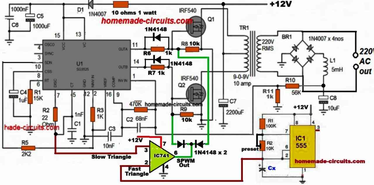
To hand absolute control over to this external LM324 auctioneer block, the SG3525 internal error amplifier must be bypassed. This is accomplished because you solder a short jumper wire directly between Pin 2 (Non Inverting Input) and Pin 9 (Compensation) of the SG3525 chip.
Wiping Out the 0.6V Diode Temperature Error: To neutralize the ambient thermal variations of the 1N4148 diodes, a 100k feedback loop resistor is wired from the shared cathode track back to the inverting input of each loop amplifier, that is Pin 6 for Voltage, and Pin 9 for Current.
When the enclosure heats up, then the forward drop of a silicon diode naturally degrades at a rate of approximately -2 mV/C.
The moment the diode drop compresses, then the voltage on the shared cathode track tries to creep slightly higher.
Since that track is coupled back to the op amp inverting input via the 100k shield resistor so the op amp instantly registers the micro volt fluctuation. It immediately backs down its native output pin, Pin 7 or Pin 8, by that exact fraction, holding the control voltage on the shared track perfectly static. This configuration turns the basic silicon diode into an Ideal Diode, yielding laboratory grade voltage stability across shifting industrial temperatures.
The Dynamics of the Auction Block: Since the cathodes are linked to the same physical node on the board, so the track can only hold a single voltage potential at any given instance.
- Under Safe Loading Conditions: The current feedback on Pin 9 sits below your preset target on Pin 10. So the current loop output Pin 8 drops low, reverse biasing its diode. The voltage loop amplifier Pin 7 sits higher, forward biasing its diode and driving the shared track to keep the inverter output perfectly flat.
- Under Overload Conditions: The moment your load tries to draw current beyond your preset limit, then Pin 9 crosses Pin 10. Then Pin 8 violently shoots HIGH. Since this voltage is higher than the voltage loop current state, so it clamps the shared track to its new potential, instantly reverse biasing the voltage diode. The voltage loop is seamlessly overridden, and the current loop pinches the SG3525 PWM to protect the primary power switches.
PCB DESIGN AND LAYOUT BEST PRACTICES
To achieve clean, glitch free execution from this high gain analog circuit, let us implement these critical routing guidelines on your PCB:
Kelvin Sensing at the Shunt: Do not mix heavy power grounds with signal grounds. Route two independent, thin traces directly from the pads of the 0.0005 Ohm sensing resistor straight back to the 100 Ohm input resistors of the green op amp. This bypasses the voltage drops that naturally occur across high current copper planes.
Handle the Unused Op Amp Stage: The LM324 contains a fourth internal amplifier with Pins 12, 13, and 14 that is not utilized in this architecture. To prevent it from picking up parasitic noise, generating internal heat, or causing weird cross talk oscillations, let us configure it as a simple voltage follower: connect Pin 14 (Output) directly to Pin 13 (Inverting Input -), and tie Pin 12 (Non Inverting Input +) directly to your system analog ground.
Decoupling Capacitors: Solder a high quality 0.1 uF monolithic ceramic capacitor (MLCC) as physically close as possible to Pin 4 (V_dd) and Pin 11 (GND) of the LM324 chip to smooth out high frequency switching EMI from the inverter power rails.
Need Help? Please Leave a Comment! We value your input—Kindly keep it relevant to the above topic!