Among the different existing inverter topologies, the full bridge or the H-bridge inverter topology is considered to be the most efficient and effective. Configuring a full bridge topology could involve too many criticality, however with the advent of full bridge driver ICs these have now become one of the simplest inverters one can build.
What's a Full-Bridge Topology
A full bridge inverter also called an H-bridge inverter, is the most efficient inverter topology which work two wire transformers for delivering the required push-pull oscillating current into the primary. This avoids the use of a 3-wire center tapped transformer which are not very efficient due to their twice the amount of primary winding than a 2-wire transformer
This feature allows the use of smaller transformers and get more power outputs at the same time.Today due to the easy availability of full bridge driver ICs things have become utterly simple and making a full bridge inverter circuit at home has become a kids play.
Here I have explained a full bridge inverter circuit using the full bridge driver IC IRS2453(1)D from International Rectifiers.
The mentioned chip is an outstanding full bridge driver IC as it single handedly takes care of all the major criticality involved with H-bridge topologies through its advanced in-built circuitry.
The assembler simply needs to connect a few handful of components externally for achieving a full fledged, working H-bridge inverter.
The simplicity of the design is evident from the diagram shown below:
Circuit Operation
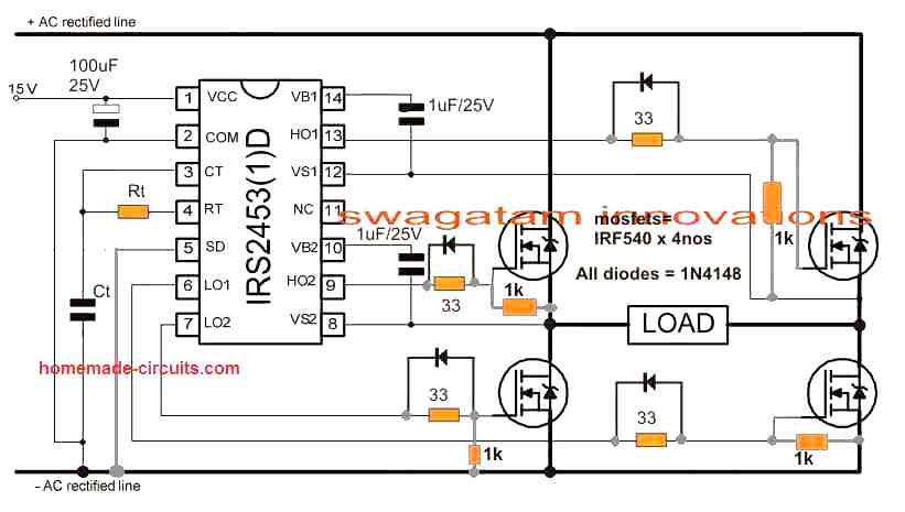
NOTE: Please join the SD pin of the IC with the ground line, if it is not used for the shut down operation.
Pin14 and pin10 are the high side floating supply voltage pinouts of the IC. The 1uF capacitors effectively keep these crucial pinouts a shade higher than the drain voltages of the corresponding mosfets ensuring that the mosfet source potential stays lower than the gate potential for the required conduction of the mosfets.
The gate resistors suppress drain/source surge possibility by preventing sudden conduction of the mosfets.
The diodes across the gate resistors are introduced for quick discharging of the internal gate/drain capacitors during their non-conduction periods for ensuring optimal response from the devices.
The IC IRS2453(1)D is also featured with an in-built oscillator, meaning no external oscillator stage would be required with this chip.
Just a couple of external passive components take care of the frequency for driving the inverter.
Rt and Ct can be calculated for getting the intending 50Hz or 60 Hz frequency outputs over the mosfets.
Important Calculations
Frequency Calculation for IRS2453 Oscillator
The IRS2453 chip uses external components Rt and Ct to set the PWM frequency.
Formula:
f = 1 / (1.453 × Rt × Ct)
- Where:
- f = Switching frequency (Hz)
- Rt = Timing resistor (ohms)
- Ct = Timing capacitor (farads)
Example Calculation:
Let us Assume Rt = 33 kΩ = 33 × 10³ Ω, Ct = 1 µF = 1 × 10⁻⁶ F:
f = 1 / (1.453 × (33 × 10³) × (1 × 10⁻⁶))
f = 1 / (1.453 × 33 × 10⁻³)
f ≈ 20.9 kHz
Thus the switching frequency is approximately 20.9 kHz. So you can adjust Rt and Ct to modify the frequency as needed.
Gate Resistors
The 33ohm resistors at the MOSFET gates limit the inrush current during switching and dampen oscillations.
Power Dissipation in Gate Resistors:
Pgate = Qg × Vgate × f
- Where:
- Qg = Gate charge of the MOSFET (63 nC for IRF540)
- Vgate = Gate drive voltage (10V)
- f = Switching frequency (20.9 kHz)
Substituting values:
Pgate = 63 × 10⁻⁹ × 10 × 20.9 × 10³
Pgate ≈ 0.013 W
Each gate resistor dissipates approximately 13 mW, which is negligible.
Power MOSFET Ratings (IRF540)
Drain-Source Voltage (VDS):
The MOSFETs must withstand the full rectified supply voltage. For a 15V input, VDS(max) must be higher than 15V. The IRF540 has a VDS(max) of 100V, which is adequate.
Current Handling (ID):
Each MOSFET handles half the load current:
ID = Iload / 2
Ensure ID(max) (33A for IRF540) exceeds this value.
Reverse Gate Diodes
The 1N4148 diodes ensures instant gate capacitance discharge for the MOSFETs, which ensures efficient switching response from the MOSFETs.
Reverse Recovery Time:
The recovery time for 1N4148 is 4ns, suitable for high-frequency switching.
Power Dissipation:
Pdiode = Vf × Iload
Where Vf = Forward voltage of the diode (0.7V for 1N4148).
Load Power
The load determines the current through the MOSFETs and resistors.
Load Current (Iload):
Iload = Pload / Vsupply
For Pload = 50 W and Vsupply = 15V:
Iload = 50 / 15 = 3.33 A
Power Dissipation in MOSFETs:
PMOSFET = ID² × RDS(on)
For IRF540, RDS(on) = 0.044 Ω:
PMOSFET = (3.33 / 2)² × 0.044 = 0.122 W per MOSFET.
Capacitor Selection
Input Capacitor (100 µF/25V):
Filters the rectified AC and smooths the supply voltage. The ripple current rating should exceed the load current (Iload).
Bootstrap Capacitors (1 µF/25V):
These provide gate drive voltage for the high-side MOSFETs. Ensure the value can handle the gate charge (Qg) of the MOSFETs.
High Voltage Feature
Another interesting feature of this IC is its ability to handle very high voltages upto 600V making it perfectly applicable for transformeless inverters or compact ferrite inverter circuits.
As can be seen in the given diagram, if an externally accessible 330V DC is applied across the "+/- AC rectified lines", the configuration instantly becomes a transformerless inverter wherein any intended load can be connected directly across the points marked as "load".
Alternatively if an ordinary step-down transformer is used, the primary winding can be connected across the points marked as "load". In this case the "+AC rectified line" can be joined with pin#1 of the IC and terminated commonly to the battery (+) of the inverter.
If a battery higher than 15V is used, the "+AC rectified line" should be connected directly with the battery positive while pin#1 should be applied with a stepped down regulated 12V from the battery source using IC 7812.
Although the below shown design looks too easy to construct, the layout requires some strict guidelines to be followed, you may refer to the post for ensuring correct protection measures for proposed simple full bridge inverter circuit.
Simple H-Bridge or Full Bridge Inverter using two Half-Bridge IC IR2110
Parts List
| Component | Value / Part Number | Description |
|---|---|---|
| IC1, IC2 | IR2110 | High and Low Side MOSFET Driver IC |
| Q1, Q2, Q3, Q4 | IRF540 or Similar | N-channel MOSFETs |
| D1, D2, D3, D4 | 1N4007 | General-purpose rectifier diodes (for bootstrap circuit protection) |
| C1, C2 | 100nF (0.1µF) | Ceramic capacitor (decoupling for IR2110) |
| C3, C4, C5, C6, C7, C8 | 22µF / 25V | Electrolytic capacitors (bootstrap and power supply stabilization) |
| R1, R2, R3, R4 | 150Ω / 0.25W | Gate resistors for MOSFETs |
| R5, R6, R7, R8 | 1KΩ / 0.25W | Pull-down resistors for MOSFET gates |
| VCC | +12V | Power supply for IR2110 |
| Logic Supply | +5V | Logic supply for control signals |
| Load Supply | VDC Load | Main DC power for the load |
| Clock Input | From Astable Multivibrator | External alternating PWM signal source |
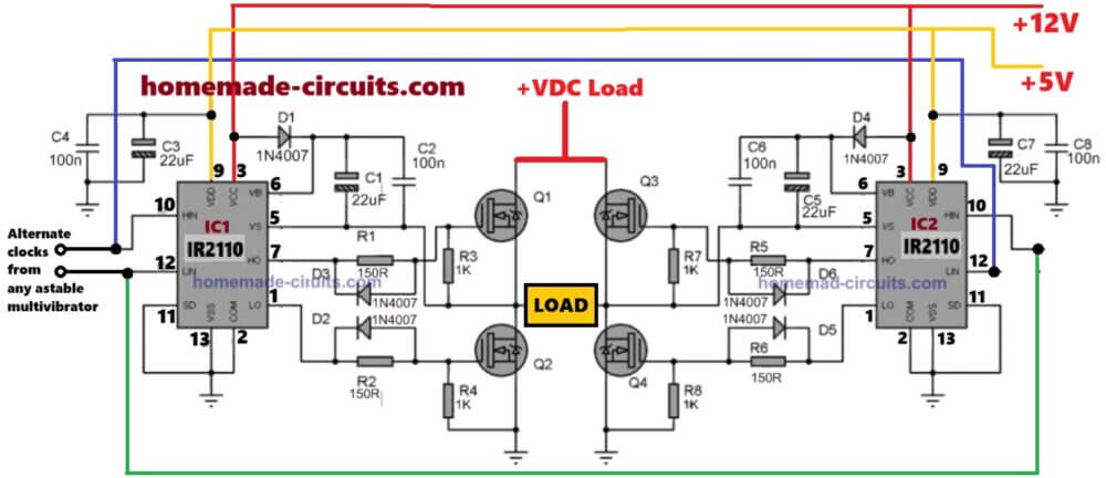
The diagram above shows how to implement an effective full bridge square wave inverter design using a couple of half bridge ICs IR2110.
The ICs are full fledged half bridge drivers equipped with the required bootstrapping capacitor network for driving the high side mosfets, and a dead-time feature to ensure 100% safety for the mosfet conduction.
The ICs work by alternately switching the Q1/Q2 and Q3/Q4 mosfets in tandem, such that at any occasion when Q1 is ON, Q2 and Q3 are completely switched OF and vice versa.
The IC is able to create the above precise switching in response to the timed signals at their HIN and LIN inputs.
These four inputs needs to be triggered to ensure that at any instant HIN1 and LIN2 are switched ON simultaneously while HIN2 and LIN1 are switched OFF, and vice versa. This is done at twice the rate of the inverter output frequency. Meaning if the inverter output is required to be 50Hz, the HIN/LIN inputs should be oscillated at 100Hz rate and so on.
Oscillator Circuit
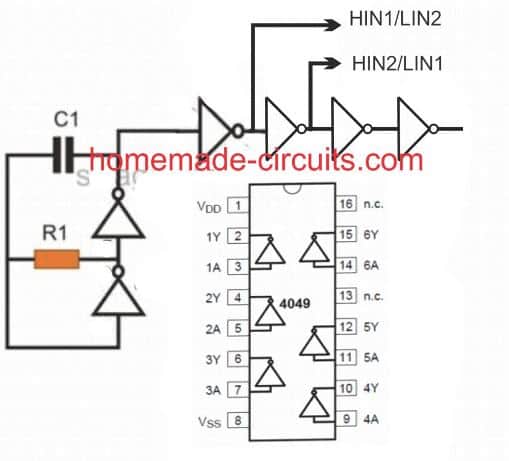
This is an oscillator circuit which is optimized for triggering the HIN/LIN inputs of the above explained full-bridge inverter circuit.
A single 4049 IC is used for generating the required frequency and also for isolating the alternating input feeds for the inverter ICs.
C1 and R1 determine the frequency required for oscillating the half bridge devices and could be calculated using the following formula:
f = 1 /1.2RC
Alternatively, the values could be achieved through some trial and error.
Discrete Full Bridge Inverter using Transistor
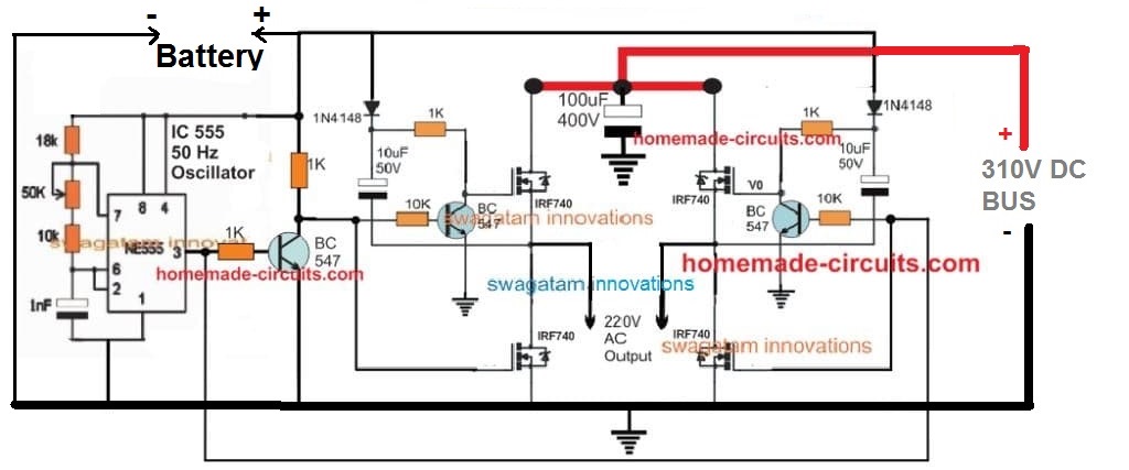
So far we have studied a full bridge inverter topologies using specialized ICs, however the same could be built using discrete parts such transistors and capacitors, and without depending on ICs.
A simple diagram can be seen below:


Questions & Answers
Hello
I used ir2153 but when I applied power the ic gets hot
can you help me ?
IC should be operated with 12V, what voltage did you use.
Hello Mr. Swagatam,
Vs1 and Vs2 isn't connected to out put directly even with high voltage.
Hello Mr.Salman, those pinouts are correctly connected as per the datasheet.
hi Swagatam Majumdar,
i want automatic switch for interchanging main supply (220 volts, 50 Hz) and stationary generator, actually i want to control my loads through computer with HMI, so i am facing problem as..
if main supply turns off that definitely my pc turns off, and also generator takes time to start so
Is it possible to start generator in such a way that my pc should not turns off and also my loads run without any interrupt?
thanks in advane
Hi Mengal,
I am sorry that won't be possible with a generator, because generators will always take sometime to start. You can opt for an UPS instead.
hi sir u r amazing…how many output watt in this circuit……plzz provide full specification….thank u .
thanks, total power will depend on trafo watts and battery ah.
hello sir
I wanted the output power to be equal to 2kW. how do I achieve that.
Also I want the output current frequency equal to 40 kHZ . How to achieve that.
Is it possible to vary the output power of the inverter?
hello akshay,
you can achieve 2kva by applying V x I = 2000 across the mosfet drain/source
Rt/Ct may be appropriately selected for achieving any desired frequency
….output power can be varied by applying a varying PWM at the "shutdown" pin of the IC.
will these types of inverters capable of driving sophisticated devices ???
How to get + and – AC rectified lines ?? You haven't mention about it
yes it's suitable for all types of equipment
first step up 12V to 220V AC using a square wave inverter, next rectify and filter this 220V Ac to 310V DC. then apply this DC across the "rectified AC line" of the above circuit.
UPTO SQUARE WAVE INVERTER IS OK.
BUT AFTER THAT HOW TO RECTIFY AND FILTTER THAT 220 V AC TO 310 V AC ?
IS IT POSSIBLE WITH A BRIDGE RECTIFIER CONFIGURATION ?
If it can be , CAN I USE 1N4007 for this purpose or should i have to use any other diodes ?
Also what is about filtering ? Can a pi-section filter do that purpose ?
yes rectify the output through a bridge network…the diodes could be 1N5402 or 6A4..the filter capacitor could be just a single 10uF/400V capacitor.
pi filter is not required
Any equivalent ICs for IRS2453(1)D ?
Can any type of MOSFET driver ic be used ?
Presently I do not have any info regarding the equivalents, but yes any type of driver with similar specs will do.
Sir if i am using a 230 / 12-0-12 300W transformer and one car battery 12 V 35 Ah for producing a minimum of 230 V AC at 60 Hz having power rating minimum to 100 W. So…
1). Could it be possible to connect this with the above circuit ?
2). Will i get a minimum wattage of 100 W by doing these ?
3). Can the output ac voltage finally produced be used to drive any sophisticated equipments ?
My purpose is that to make a pure sine wave inverter suitable for operating the HOME THEATER in my CAR without making any humming noise while operating the System…
I am not interested to make modified inverters based on PWM concepts, since they require a better mean such as OSCILLOSCOPE to display and analyze the wave forms formed…
Arun,
for the above design you will need a two wire transformer not a center tap type…0-12V will do, or 0-9V
Without PWMs, a sine wave is not possible.
you can try putting a 1uF/400V capacitor and a 3amp 1mH inductor approx at the output of a square inverter for reducing the hum.
wattage of an inverter solely depends on the transformer wattage and the battery AH, driver circuits have nothing to do with it.
where did you buy the IRS2453(1)D? because I can not find it.
Hello
Eng,Swagatam.
Is the above inverter circuit diagram modified sinewave or pure sinewave
inverter. And also, is it possible to power inductive and sophiscated
device without problem?
Hello Raphael,
it's a simple square wave inverter, it can be converted into a sine wave by inducing PWMs at the gates of the lower mosfets.
Thank you for your quick reply.
But can you pls give me a simple circuit on PWMs that needs tobe connected to the lower gates of the mosfets.
You can use the PWM design which is shown in the second diagram of the following link
https://www.homemade-circuits.com/2013/04/how-to-modify-square-wave-inverter-into.html
The section consisting of T5/T6 is the PWM stage.
I wonder why there are no snubber circuits? Most kinds of electronic high power switches I've seen have snubbers to protect the FET's or IGBT's.
the fets alerady have in-built snubbers, but you can always add more externally for reinforcing the inbuilt ones…
hello, swatagam majundar, inverter circuit on the waveform what? sine or square and how the power output?
thank you.
hello Robet, it's squarewave
Hello sir
His ic seems powerful and I think we can add pwm to the low side of the driver going to the gates but my question is this.
You said that the gate voltage has to be at least 5v higher than drain voltage for the high side to function properly so now if I power the drain with a +24vdc supply and then use a 12v regulator to power the IC at pin 1, will sufficient voltage come out at the pin 13 and 9 high side output.? To work sufficiently.
2)Also when using a 24vdc supply and 12 DC at pin 1 of the IC the 1uf/25v caps at 14 and 10 can it be increase to a higher capacitance/voltage?
Hello Michael,
with a 12V as the supply to the IC the output at the high side pin would be 36V, which would imply an efective12V at the respective mosfet gate, which would be sufficient for driving the gate optimally.
the capacitor voltage rating is relevant to the supply voltage so I think it can be selected to be 25V
capacitance value are OK, no need of increasing it.
Also sir one important question.
Now using pwm we make it as close to a sine wave as possible but for a 12 supply we would need a 0-12/220v trafo but for pwm should it still be 0-12/220 or 0-7/220v to make up for the PWM sectioj just like in the center tap sine wave pwm inverters you have.
for a PWM insertion, the trafo voltage should be lower than the supply voltage to compensate the PWM range
Also sir pls I still don't get how full bridge works fully.
Could you explain what happens during the low and high side in terms of conducting. I think the low side MOSFET switch according to wave form at its gate but high side?
the diagonal mosfets pairs are switched ON simultaneously, while the left and the right pairs switch ON alternately, generating the required AC across the connected trafo primary.
while the diagonal mosfet switch ON, the high side mosfet is applied with an excess of 5 to 10V than its drain voltage so that it's able to switch ON fully and compliments the low side mosfet, making the conduction complete and full.
Hello sir,
I now understand am gratefull.
I have one more question
In push pull config, if I wanted more power output say from 500w to 2000w output I simply add more MOSFETs in parallel and its easier since we only deal with low side switching but now since full bridge uses four MOSFETs,
Once I have my trafo say 0-12/2000w ready,
How do I increase power output using h bridge (full bridge topology)
Basically what do I so to increase power from say 500w to 2000w?
Do I add MOSFETs to both low and high?
Confused.
Hello Michael, for an Hbridfge also you will need to add mosfets in parallel for multiplying power output…the rule is same…however you can alternatively decide on a higher voltage trafo…like a 48V primary trafo, and a 48V battery for the boosting power without having to use more number of mosfets.
…yes add more number of mosfets with each of the four existing mosfets
Hello Sir
Just to be clear, if i have an N channel MOSFET that gives out 300w.then I use four of this on h bridge config.(2 on high and 2 on low side) then my total output should be 1200w right?
Hello micahel, no all the 4 together will help to produce 300 watts only, because the diagonal ones are conducting in series, so no question of power addition, while the left and the right diagonal pairs are conducting alternately.. so again no chance of power adding up.
.
Remember Power=Voltage times current
If the Voltage across the FET is 1 Volt when on and the current rating is 300 amps that's 300 watts per FET that is on, at a 50% duty cycle, and if the output source is 12 volts after you subtract the FET voltage drops, that's 3600 watts output. total power consumption from source supply is ~ 4200 watts.
Hello Sir
That means that the only down side to the h bridge would be that I would require double the amount of MOSFETs I would use for a push pull config.
Example if I use these four N channel on push pull by using two per each side of push pull then at 300w per MOSFET then I would have 600w output. But for h bridge when diagonal are conducting the two diagonal are only supplying 300w when individually they can give 300w each and this is due to the series connection so to get 600w in h bridge I would use 8 n channel MOSFETs.
Is my calculation correct according to your explanation?
Michael, you are correct….but the H bridge trafo can be significantly smaller compared to a center tap topology…so it wins here, moreover you have the option of using higher voltages (upto even 60V or 100V) and get massive power outputs (kvas) without adding a single mosfet to the existing 4.
Hello sir,
The thing is I can afford to get two 12v batteries that's why I am planning to use 24v input but you just mentioned using higher voltage like 60v or up to 100 but that would mean I have two options
1) using more batteries which I don't want to as more is expensive
2)using a DC to DC converter
Now If I use option 2 as option 1 is ruled out, it means more components added as I have to use oscillator like sg3524 and a small ferrite trafo (puah pull converter) which honestly means component count is getting higher.I don't want that as I want simplicity
A) So I was thinking are there DC to DC converters that employ minimal components only and yet so simple and effective that I can use to convert 24v to 48v.?
B) so if (A) is possible then I connect it to the h bridge, since diagonal high and low side MOSFETs conduct then when at full power the low MOSFETs will conduct a lot of current but my question is since the high side will also conduct current will the transformerless DC to DC converter withstand such current draw at full load to adequately complement its diagonal low side MOSFET.
Hope you get where am coming from.I have seen h bridge inverters using push pull DC to DC converters whose output powers the drain of the mosfets high side but since the transformers are small yet current will flow through them when conducting.
So basically it seems the DC to DC has to be able to output certain amount of current?
Hello sir
If complications arise I will stick to 24v direct from battery input and use as much MOSFETs as possible.I don't want complicated process.
Unless you have a transformer less solution with stable output voltage. Ha ha
Hello Michael,
using a DC DC converter would be like using two inverters in series which could make the system inefficient….moreover to produce 25 amps from the DC t DC converter could be a complex affair as it would require heavy duty coils and mosfets involved.
so it's better to go with a 24V battery directly with the designed inverter and use more mosfdets if required.
Hello sir
Is it completely safe to apply pwm to only low side of MOSFETs in full bridge only especially in this circuit where I would like to use your pwm circuit.?
I am asking because i have been studying other drivers like the ir2110 which is another IC I am thinking of using as a back up if I can't find ir2453
Now the thing is to implement full bridge using ir2110 I will need to use two of the IC's and then connect the lowside input LIN of ic1(ir2110) to the the high side input HIN of ic2(ir2110) so that that way diagonally they botje turn on causing current to flow but the catch here is that both inputs will receive PWM pulses( chopped 50hz pulses) so this means using the ir2110 the high side output will trigger the high side MOSFET as well as the low side mosfet with this pulses but I want to know it it will be suitable to drive the high side sufficiently.
With this simple ir2453 we can just leave the high side pulse at line frequency (50hz) while we just pass PWM to low side only whixh is why I find it desirable as it saves lots of space and stress.
But my main queation again is will both techniques be ok . just increasing my options.
Hello Michael, you can isolate the PWMs by adding a diode and a resistor across the respective LIN pinouts of the both half-bridge ICs, or alternatively you can prefer applying the PWMs at the gates of the low side mosfets for the same.
Hello sir,
I forgot to mention that I sent you a mail.
I'll check it as soon as i finish with my website's pending assignments…