Interested to make your own power inverter with built in charger? A simple 400 watt inverter circuit with charger that can be very easily built and optimized has been provided in this article. Read the complete discussion through neat illustrations.
Introduction
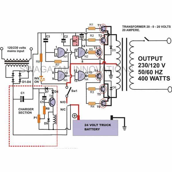
A massive 400 watts power inverter with built in charger circuit has been thoroughly I have explained in this article through circuit schematics. A simple calculation to evaluate the transistor base resistors has also been discussed.
I have discussed the construction of a few good inverter circuits through some of my previous articles and am truly excited by the overwhelming response that I am receiving from the readers. Inspired by the popular demand I have designed yet another interesting, more powerful circuit of a power inverter with built in charger.
The present circuit though similar in operation, is more interesting and advanced due to the fact that it has got a built-in battery charger and that too fully automatic.
As the name suggests the proposed circuit will produce a massive 400 watts (50 Hz) of power output from a 24 volt truck battery, with an efficiency as high as 78%.
As it’s fully automatic, the unit may be permanently connected to the AC mains. As long as the input AC is available, the inverter battery is continuously charged so that it is always kept in a topped up, standby position.
As soon as the battery becomes fully charged an internal relay toggles automatically and shifts the battery into the inverter mode and the connected output load is instantly powered through the inverter.
The moment the battery voltage falls below the preset level, the relay toggles and shifts the battery into the charging mode, and the cycle repeats.
Without wasting anymore time let’s straightaway move into the construction procedure.
Parts List for the circuit diagram
You will require the following parts for the construction of the inverter circuit:
All resistors are ¼ watt, CFR 5%, unless otherwise stated.
- R1----R6 = To be calculated - Read at the end of the article
- R7 = 100K (50Hz), 82K (60Hz)
- R8 = 4K7,
- R9 = 10K,
- P1 = 10K,
- C1 = 1000µ/50V,
- C2 = 10µ/50V,
- C3 = 103, CERAMIC,
- C4, C5 = 47µ/50V,
- T1, 2, 5, 6 = BDY29,
- T3, 4 = TIP 127,
- T8 = BC547B
- D1-----D6 = 1N 5408,
- D7, D8 = 1N4007,
- RELAY = 24 VOLT, SPDT
- IC1 - N1, N2, N3, N4 = 4093,
- IC2 = 7812,
- INVERTER TRANSFORMER = 20 – 0 – 20 V, 20 AMPS. OUTPUT = 120V (60Hz) OR 230V (50Hz),
- CHARGING TRNASFORMER = 0 – 24V, 5 AMPS. INPUT = 120V (60Hz) OR 230V (50Hz) MAINS AC
Circuit Functioning
We already know that an inverter basically consists of an oscillator which drives the subsequent power transistors which in turn switches the secondary of a power transformer alternately from zero to the maximum supply voltage, thus producing a powerful stepped up AC at the primary output of the transformer.
In this circuit IC 4093 forms the main oscillating component. One of its gates N1 is configured as an oscillator, while the other three gates N2, N3, N4 are all connected as buffers.
The oscillating outputs from the buffers are fed to the base of the current amplifier transistors T3 and T4. These are internally configured as Darlington pairs and increase the current to a suitable level.
This current is used to drive the output stage made up of power transistors T1, 2, 5 and 6.
These transistors in response to its alternating base voltage are able to switch the entire supply power into the secondary winding of the transformer to generate an equivalent level of AC output.
The circuit also incorporates a separate automatic battery charger section.
How to Build?
The construction part of this project is pretty straightforward and may be completed through the following easy steps:
Begin the construction by fabricating the heat sinks. Cut two pieces of 12 by 5 inches of aluminum sheets, having a thickness of ½ cm each.
Bend them to form two compact “C” channels. Drill accurately a pair of TO-3 sized holes on each heat sink; fit the power transistors T3---T6 tightly over the heat sinks using screws, nuts and spring washers.
Now you may proceed for the construction of the circuit board with the help of the given circuit schematic. Insert all the components along with the relays, interconnect their leads and solder them together.
Keep transistors T1 and T2 little aloof from the other components so that you may find sufficient space to mount the TO-220 type of heat sinks over them.
Next go on to interconnect the base and emitter of the T3, 4, 5 and T6 to the appropriate points on the circuit board. Also connect the collector of these transistors to the transformer secondary winding using thick gauge copper wires (15 SWG) as per the shown circuit diagram.
Clamp and fix the whole assembly inside a well ventilated strong metallic cabinet. Make the fittings absolutely firm using nuts and bolts.
Finish the unit by fitting the external switches, mains cord, output sockets, battery terminals, fuse etc. over the cabinet.
This concludes the construction of this power inverter with built in charger unit.
How to Calculate Transistor Base Resistor for Inverters
The value of the base resistor for a particular transistor will largely depend on its collector load and the base voltage. The following expression provides a straightforward solution to calculate accurately the base resistor of a transistor.
R1= (Ub - 0.6)*Hfe / ILOAD
Here Ub = source voltage to R1,
Hfe = Forward current gain (for TIP 127 it’s more or less 1000, for BDY29 its around 12)
ILOAD = Current required to activate fully the collector load.
So, now calculating the base resistor of the various transistors involved in the present circuit becomes pretty easy. It is best done with the following points.
We start first by calculating the base resistors for the BDY29 transistors.
As per the formula, for this we will need to know ILOAD, which here happens to be the transformer secondary one half winding. Using a digital multimeter, measure the resistance of this portion of the transformer.
Next, with the help of Ohms law, find the current (I) that will pass through this winding (Here U = 24 volts).
R = U/I or I = U/R = 24/R
- Divide the answer with two, because the current of each half winding gets divided through the two BDY29s in parallel.
- As we know that the supply voltage received from the collector of TIP127 will be 24 volts, we get the base source voltage for BDY29 transistors.
- Using all the above data we can now very easily calculate the value of the base resistors for the transistors BDY29.
- Once you find the value of the base resistance of BDY29, it will obviously become the collector load for TIP 127 transistor.
- Next as above using Ohms law, find the current passing through the above resistor. Once you get it, you may go on to find the value of the base resistor for the TIP 127 transistor simply by using the formula presented at the beginning of the article.
- The above explained simple transistor calculation formula may be used to find the value of the base resistor of any transistor involved in any circuit
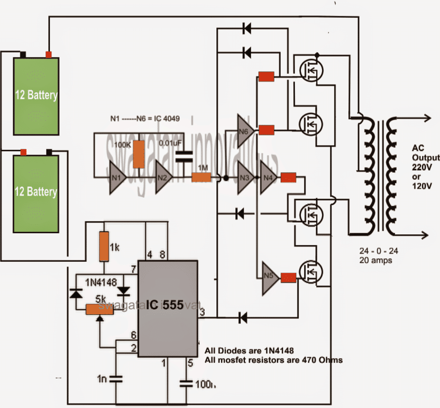
Designing a Simple Mosfet Based 400 Watt Inverter
Now let's study yet another design which is perhaps the easiest 400 watt sine wave equivalent inverter circuit. It works with lowest number of components and is able to produce optimum results. The circuit was requested by one of the active participants of this blog.
The circuit is not actually a sine wave in true sense, however it's the digital version and is almost as efficient as its sinusoidal counterpart.
How it Works
From the circuit diagram we are able to witness the many obvious stages of an inverter topology. The gates N1 and N2 form the oscillator stage and is responsible for generating the basic 50 or 60 Hz pulses, here it has been dimensioned for generating around 50 Hz output.
The gates are from the IC 4049 which consists of 6 NOT gates, two have been used in the oscillator stage while the remaining four are configured as buffers and inverters (for flipping the square wave pulses, N4, N5)
Until here, the stages behave as an ordinary square wave inverter, but the introduction of the IC 555 stage transforms the entire configuration into a digitally controlled sine wave inverter circuit.
The IC 555 section has been wired up as an astable MV, the 100K pot is used for optimizing the PWM effect from pin#3 of the IC.
The negative going pulses from the IC 555 are only utilized here for trimming the square wave pulses at the gates of the respective MOSFETs, via the corresponding diodes.
The MOSFETs used may be any type able to handle 50V at 30 amps.
The 24 batteries need to be made out of two 12V 40 AH batteries in series. The supply to the ICs must be provided from any of the batteries, because the ICs will get damaged at 24Volts.
The 100K pot should be adjusted using an RMS meter for making the RMS value at the output as close as possible to an original sine wave signal at the relevant voltage.
The circuit has been exclusively developed and designed by me.
Feedback from Mr. Rudi regarding the waveform issue obtained from the above 400 watt inverter circuit
hi sir,
i need your help sir. i just finished this circuit. but the result is not as what i expected, please refer to my pictures below.
This is the wave measure from the gate side (also from the 555 and 4049 ic): it look just nice. freq and duty cycle almost at desire value.
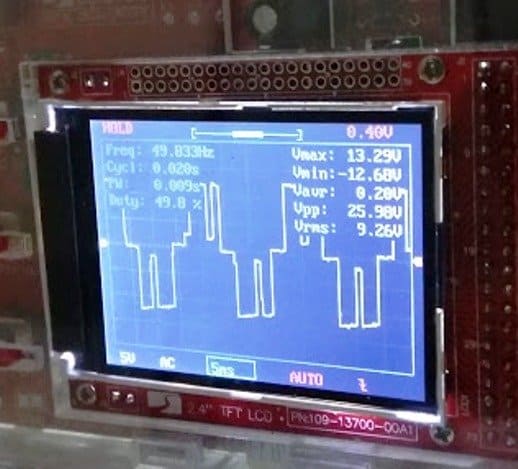
this is the wave measure from mosfet drain side. everything is mess up. freq and duty cycle are changes.
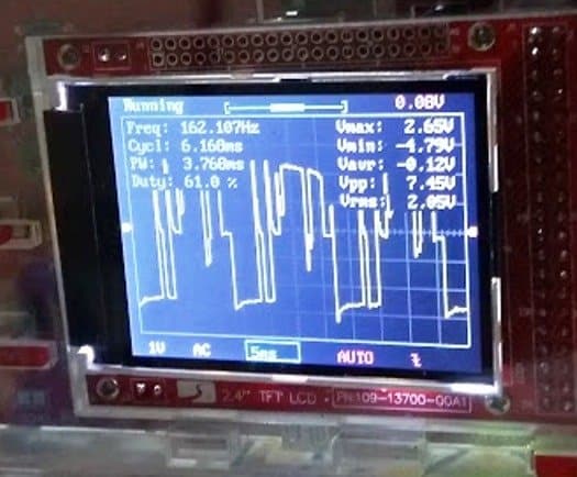
this is i measure from output of my transformer (for testing purpose i used 2A 12v 0 12v - 220v CT).
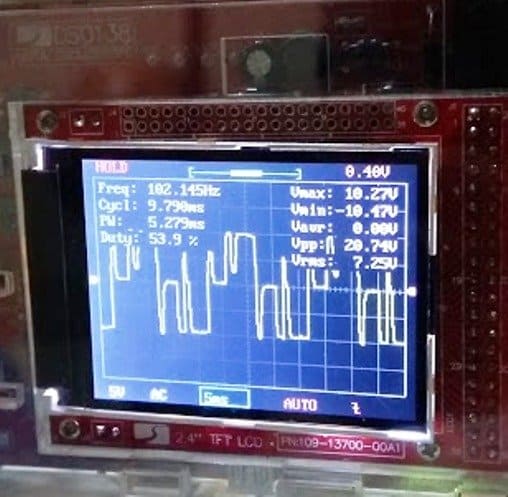
how to get the transformer output wave just like a gate one? i have a ups at home. i try to measuring the gate, drain, and transformer output. the waveform is almost the same on that small ups (modified sinewave). how do i achieve that result in my circuit?
please kindly help, thanks sir.
Solving the Waveform Issue
Hi Rudi,
it's probably happening due to transformer inductive spikes, please try the following:
first increase the 555 frequency a bit more so that the "pillars" across each square wave cycles look uniform and well distributed..may be a 4 pillar cycle would look better and more atable than the present waveform pattern.
connect a large capacitor, may be a 6800uF/35V right across the battery terminals.
connect 12V zener diodes across gate/source of each of the mosfets.
and connect a 0.22uF/400V capacitor across the transformer output winding....and check the response again.

Questions & Answers
I have another question about this circuit. Since this is drawn for a 400w and I’m needing 1k or more, like 1.2 kw to 1.5kw, maybe even 2 kw. I’m thinking the .22 uf across the output windings needs to be increased say to .47uf or would it be better to use a .22 across each output of each transformer if I used paralleled pieces keeping those as close to the transformer as possible. I know the capacitance should not be really high on the AC side unless there are bleed resistors across the terminals. Then I’m not sure what value those would have to be. Maybe near 1M or slightly lower. I suppose testing with a scope would tell. But then if the R is not suitable that may cause some rather serious issues when the wave wants to reverse flow. I have an unfinished inverter driver board I got on line from an ebay seller that is nearly finished and still needs an xformer made for it. It uses one of those EGS002 SPWM driver modules. The hold up on that has been finding a suitable toroid core or E core, again, not sure which would be better. As soon as I can afford to get some cores to work with I hope to finish this inverter project. I have a whole bunch of 14 g enameled wire on spools so I could either use some of that or get some smaller G wire which would for sure be easier to work with, but since the primary winding doesn’t need a lot of turns for a high freq, inverter it shouldn’t be a big deal. I’m going to order some braided sleeve insulation soon to cover those primary turns to keep them away from the secondary high V to reduce heat transfer issues.I’m figuring the primary turns should be on the outside for better cooling no matter which core I use. That inverter I had that took the lightning bolt hit had the primary turns on the inside of the windings and I could see signs of heat damage from before the circuit board went up in smoke and charcoal. I was using that inverter to run a table saw and power tools when I was building my old cabin. That was a 2kw modified wave unit and it was just about maxed out on the table saw and sometimes the circular saw would be too much for it when the saw would get loaded up hard for too long.
I used around 3uF/400V at the output of the following modified design which turned the output into almost a pure sine wave:
I want to give this a try but unfortunately for now, I don’t have a 9-0-9 xformer to 120v for testing. I do have a 6-0-6 to 120 so I think I would have to use a Vreg in here, not sure if that would be workable thing though as it would have to have a series pass Q to handle the current required, but then the xformer is a really low current output rating so it may be Ok. under 500 Ma’s. So it would have to be a 5v reg as that’s all I have on hand now. The other thing is what needs to be done to the circuit to change it to 60 hz? The 5k pot will control the duty cycle of the 555 so a capacitor and or a resistor needs to be changed on the timing section. I guess I need to go to the 555 calc and work this out.
Instead of the above concepts, I would rather suggest you to try the following modified inverter design which will produce much improved output waveform than the above designs:
You can use a 6-0-6 transformer for this design provided the battery suply is 12 V.
Hi Swagatam and Rudi mostly. My question is actually for Rudi. I’m wondering if the wave form was ever made better for this 555/4049 MOSFET inverter? I have ben looking at different circuits to make inverters and wish to build an inverter to power a class AB audio amp to put in my car stereo hopefully. I won’t need standard freq. 50/60 hz but will need 0v center tap to give dual supply AC to run amp which has bridge rectification in the power input section. Actually there are a couple of different schematics I’m looking at and IRC one or more can take 32-0-32 dual rail DC or AC. One or 2 may be p to using 90-0-90 v too. One of the amps is supposed to be 300+300 w and that’s the one I really want to use to power speakers @150w. I’ve read it’s better to have an amp that can over power the speakers than 1 that is under power. Safer for the speakers as long as the coils can handle the heat. That’s all another factor from this post though. It’s the correct voltages from the output that make the biggest issue. I can deal with that when I wind the transformer. As I said at the beginning of this message, I’m concerned about getting the wave form cleaned up. I just recently acquired my Tektronix TDS210 which was a non starter but I got the parts needed to revive it and now it’s working so I can go to work on stuff now as soon as I get enough space to work on stuff. The motorhome is too small to pull out all the electronic stuff and build on the dinning table. Please send up dated email, ITMT I guess I will get started with something and see what happens. So many unfinished projects before the scope was salvaged and now it’s a motivation issue. Along with a money issue. I have some ferrite cores I’m looking at now to wind, will try for those next month hopefully.
Thank you Bret,
If you would be using a bridge rectifier to rectify and then filter the AC, then I think the AC waveform won’t matter much. Because once the AC is rectified and filtered with a capacitor all impurities would be eliminated.
Well it would seem so, but I have read some about noise still getting through in DC ripple and then there is some RF interference in some cases. Zeners generate their own noise, really sensitive circuits can even pick up EMI and since this an amp, I’m pretty sure any noise anywhere in the circuitry will be amplified along with everything else. Maybe I’m wrong here, I don’t know at this time. This brings me to something I saw in my email from another fellow that made a statement the electronics was easy to learn and another fellow set him an angry email telling him if it was easy, why did he spend all that time in tech school learning and then all the time he spent in the field working, fixing and still learning, no one knows everything about electronics. I just finished building the circuit for the over temp detection and it’s not all that complicated, a rather simple project that so far has frustrated me. It all seems to ohm out correctly, the Q is good. I didn’t include the relay with its coil in the project as yet and the LED stays on all the time no matter where the 10k pot is set in conjunction with the 33k and 10k NTC voltage divider section. At this point like many other projects I have attempted and so far failed at, I’m going to move on for now.
OK I understand, however if filter capacitors and EMI filters are not able to stop the RF frequencies then nothing in this world can stop them. The capacitive filters and the EMIs are our only hope.
I have seen how you are helping people here,thank you for that….I have a 400w 12v sinewave inverter that has its transistors spoilt…I don’t know its transistor specifications and would like your help on how to choose its specification…please reccomend which transistor is more favorable in this occasion,thank you.
MOSFET
I think the following article might help you to understand the right way of calculating MOSFET power for inverter applications:
https://www.homemade-circuits.com/how-to-calculate-and-match-inverter/
thanks
What type of transistor is used in the inverter, MOSFET or BJT?
Sir, can you explain more, does this battery becomes back-up power supply when the AC mains is gone,and when the AC comes back it will be charged again?
Khem, yes the battery works like an automatic power back up but you will have to keep SW1 switched ON for that.
Or alternatively you can simply remove the Sw1 and join the points with a wire link….and put the switch across the NO and NC contacts of the relay, which will allow you to bypass the relay and operate the inverter even if the battery is not exactly fully charged.
Hello sir,
I have a quick question about the circuit “How to Build a 400 Watt High Power Inverter Circuit”. There is an component in the circuit which looks like a diode but it is not. You mention as INV ON and it is connected to R8 and the sw1. In the diagram, it is close to the diode array which is connected to the transformer. Could you please tell me what is that component?
Regards,
Jose Salazar
Hi Jose, that’s an LED, it will light up indicating the inverter mode is ON…
Sir, Please provide me the same function (i.e Built in charger for battery) inverter circuit for 12V battery
Raj, you can use the same circuit for a 12V battery also, just make sure to use a 12V battery for the charger section, and also the 7812 IC will not be required in that case, and 12V will need to be used in the formula for calculating the transistor resistors. Relay will also change into a 12V relay
Sir good afternoon I made 400W inverter using 4093 IC.Sir I have a doubt in diagram is red line in diagram connected to input of regulator after switch connected to emitter of TIP127 transistor also will be thankful if u reply I have made inverter but output is only 40V A/C I used a autotransformer for connection as battery for checking output of inverter
Dweep, the red line is the positive line from the battery via the switch S1….Please use a proper step-down transformer in reverse for getting 220V output…auto transformer will not work here
Thanks for reply Sir it’s Darlington pair so it’s a high current gain amplifier should it not be reversed with supply given to collector and output at emitter of TIP 127 but anyway s circuit I made I didn’t connect it only what’s your opinion about it
Dweep, TIP127 is a PNP transistor, so the positive will be on the emitter, and the shown connections are correct!
Sir doubt about the emitter of tip127 connected to supply line is there a jump or are the emitter s of tip 127 just connected to each other.
The TIP127 emitters are directly connected to the positive line.
Sir Dweep here thanks for reply I have used a variable dc supply using dimmer instead of battery u meant to say it could be a reason for not getting desired output.
Sir supply line is connected via switch directly to 0 of 20-0-20 transformer or it has a joint to TIP127 transistor too.
Dweep, please see it carefully, all the inter-connections which are not connected are shown with curved jumper symbol, rest all the intersections are connected.
Dweep, The input supply to the inverter can be any DC, but it should have over 5 amp current, and the voltage should be higher than the transformer primary voltage…if the transformer voltage is 9-0-9, then the input supply should be 12V minimum.
Hello Sir,can you give me the values of the resistors 1 thru 6 then i can check my calculations
i blow up already some tansistors
i use de dec3716 (5of them in 1 section) and the bdx53 in a little different confuguration
thanks
rinus
Rinus, R5, R6 can be 10K, the other will need to be calculated as per the transformer rating
My transformer is primair 110 and 2*12V 40A
i’m stack with the calculations
pls help me
you can give me the values you use as an example
thanks
R = (Ub – 0.6) x Hfe / ILOAD
= (12 – 0.6)10 / 40 = 2.85 ohms
you can try 10 watt resistor.
thank you very much
great job
ONLY TIP35 IS used instead of BDY29. One more question is that any other changes is required or not?
yes, that’s right, rest can be as it is.
Forget to say what is the value of R1 to R6?
you can use 10K 1/4 watt
sorry it is for the gate outputs only, for the power transistor base you will have to calculate as per the given formula
sir if i use invertor transformer 12-0-12/30 amp and battery is 12v,then any problem is happened or not? Actually,Iload is simply 30amp.Thats why i am thinking that transistor & diode is capable to withstand or not this against 30amp.That is the my question.
Sanjib, you can use 12/30amp trafo with a 12V battery, and instead of BDY transistor you can use TIP35
Please sir tell me if i changes some & there are give below
1)if i use invertor transforMER 12-0-12/ 20amp or 30 amp & Charging transformer 0-12/3amp or 5 A
2) Battery voltage is 12v /100AH
3)What is the value of R1 to R6 ,i cannt calculate because of Iload? what is ILOAD value?
After using this ,the o/p will be 400w or not.If not what should made changes for this circuit?
Plsease reply.
Sanjib, you can use any transformer as per your own preference, as long as the supply to the circuit section is 12V, and as long as the battery voltage matches the trafo voltage there won’t be any issues.
ILOAD can be achieved by dividing the trafo wattage with the battery voltage, in your case that will be simply 20 amps I guess
Pls can i charge d battery as d inverter circuit z running as itbworks in cars
Hi Mr swagatam please how do one determine the capacity of inverter after production
Sir,
What type of simple Inverter can i desing to operate Fans, bulb, Soldering Iron and Tv/dvd?
Lets say, the one with 220v 50hz, 150watt.
I need your help on, partlist needed for the above invater construction.
Thanks!
Aminu, you can try the last circuit from the following link:
https://www.homemade-circuits.com/2013/04/how-to-modify-square-wave-inverter-into.html
How would I go about doubling the wattage rating to 800w?
more transistors in parallel with the NPN transistors