In this article I have explained how an input AC source could be increased to any desired levels using simple voltage multiplier circuits, built with capacitors and diodes.
Thus the basic function of a voltage multiplier circuit is to multiply a given AC voltage source to any higher desired level, simply by adding the relevant number of diode/capacitor stages.
The use of diode-capacitor combination to double voltage is a popular idea.
Cascading of voltage doublers, on the other hand, could be used to generate incredibly high DC voltages using normal home AC voltages.
How Rectifiers are Configured for Peak Voltages
Let us look at how both positive and negative half-wave rectifiers are used to generate peak voltage from an AC source. This peak voltage further stepped up using half wave voltage doublers and full wave voltage doublers and also other voltage multipliers.
The below shown Figure "a" depicts a positive-output half-wave rectifier, whereas Figure "b" depicts the identical copy with a negative output, and Figure "c" depicts a dual voltage doubler integrated into a full-wave voltage rectifier.
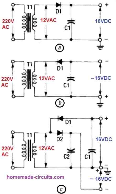
The combination of capacitors and diodes cause the input AC to reach their peal levels, which can solved using the following formula:
Peak Voltage = RMS AC x 1.41
In the above examples, 12V AC is used as the source RMS voltage. Using this value in the above formula gives us the respective peak level of the 12C RMS, as shown below:
Peak Voltage =12 x 1.41 = 16.92V
Now, as we know how rectifiers are used to generate peak level voltages from an input AC source, I have explained how the above circuit are enhanced as voltage multipliers, through the following examples.
Half Wave Voltage Doubler
The figure below depicts a half-wave voltage doubler; we'll imagine C1 and C2 are discharged at the start. The top input wire is positive and the lower input wire is negative during the first half-cycle as depicted in the diagram. Thus D1 conducts and C1 charges to roughly 170 volts peak.
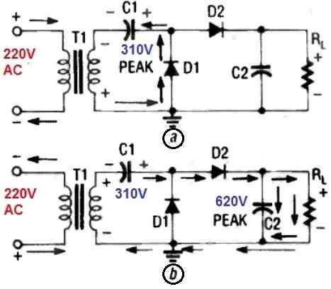
Because reverse-biased diode D2 cannot conduct, C2 discharges via RL. The process is identical in the second half-cycle (b), apart from the fact that D2 conducts and C2 charges.
The circuit functions as a voltage amplifier without the need of a transformer. Although T1 could offer isolation and boost the AC voltage coming into the doubler at first, the amplification caused by the doubling operation could proceed even if T1 was not there.
Once the polarity is reversed, both the input voltage and the charge across C1 are connected in series, yielding a peak voltage of roughly 340 volts. A half-wave doubler, on the other hand, cannot be employed with a load that consumes a lot of current.
Full Wave Voltage Doubler
The full-wave voltage doubler in the figure below has been redesigned for simplicity; it has better regulation and is simpler to filter compared to the half-wave version.
The circuits shown above generates approximately twice the 310 volt peak AC voltage, or around 620 volts peak across RL. D2 is turned off during the first half-cycle (a), and D1 conducts, resulting in a Vc of roughly 310 volts DC.
The positive voltage is substituted by a negative voltage on the subsequent half-cycle (b), causing D2 to conduct and D1 to be switched off. RL connects C1 and C2 in series, essentially doubling the voltage to around 620 volts DC.
The full-wave voltage doubler, unlike the half-wave variant, contains a couple of capacitors across RL instead of one. C1 in Fig. 1 is cut off and not supplied for half of every cycle, whereas C1 and C2 in Fig. 3 are alternately supplied.
When the capacitor associated to the cut-off diode discharges, could only do so by the way of the capacitor getting supplied, resulting in a modest reduction in both current and peak voltage.
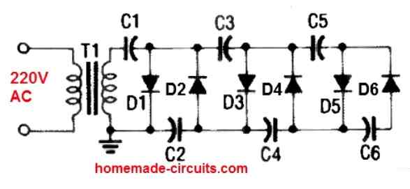
Cascaded Voltage Doublers
The following figures depict cascaded type of voltage doublers. The diagram shown below is the most basic form of cascaded voltage multiplier design. If you make it, employ 1N4007 diodes rated at 1 kilovolt peak in-verse voltage (PIV) for D1-D6, and 0.068 uF-0.1 uF capacitors rated at 400 volts DC operating voltages.
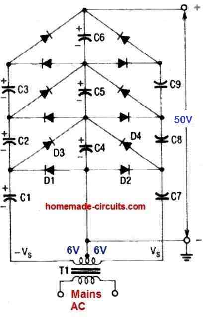
Cockcroft-Walton Multiplier
A Cockcroft-Walton or Greinacher cascaded voltage multiplier, as shown in the figure below, is an expanded variant of the above, that is more stabilized for medium current applications.
The input AC is supplied from a step down transformer with a secondary center tap winding of 6-0-6V.
How to Calculate
It is easy to calculate the output voltage from a Cockcroft-Walton voltage multiplier using the formulas discussed below:
Any number of stages may be added to this circuit. The no-load output voltage is equal to two times the peak input voltage multiplied by the number of stages N, or the peak-to-peak input voltage jump (Vpp) times the number of stages:
Vo = 2NVp = NVpp
The number of stages is directly proportional to the number of capacitors connected in series (in single line) from the output to ground.
In the above shown example, the input is 6V AC RMS for every half cycle, and there are 3 multiplier stages. Therefore the high output voltage could be calculated in the following manner:
Vo = 2NVp
= 2 x 3 x (6 x 1.41) = 50.76V
The 6 x 1.41 is the peak voltage calculation for the 6V RMS.
Alternative, the above could be also calculated in the following manner:
Vo = NVpp
= 3 x (12 x 1.41) = 50.76
Both the formulas provide us the same results for the above diagram.
Corona Wind from Cascaded Voltage Multiplier
To make "corona wind," you can make use of a sewing needle as an emitter for the Cockcroft-Walton voltage multiplier as depicted below. The output from this needle sharp end will simulate a hissing sound. Theis hissing sound resembles the sound of light cool breeze or wind. and is thus called corona wind.
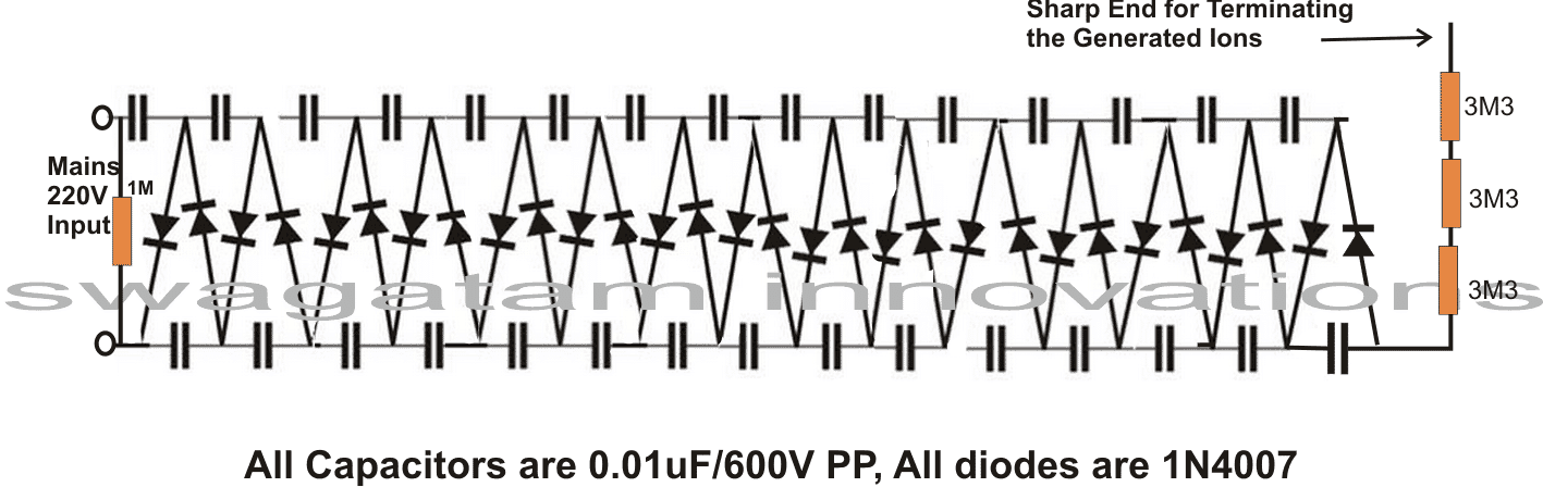
While powered from 120 volts AC, the circuit produces 3.75 kilovolts DC, and when supplied from 240 volts AC, it produces 7.5 kilovolts DC. For safety sake, a cascaded voltage doubler's output must be terminated with at least 200 megohms resistor before being permitted to protrude outside a secure plastic casing.
Cascaded voltage doublers are often used to create voltages as high as 5 megavolts DC, particularly when dealing in a pressured environment.
The main benefit of employing voltage doublers is that they can be built with low-cost low-voltage components. Or else, you'd have to use costly and fairly big capacitors like the one illustrated in Fig. 9 if all of the components had to be of the high-voltage type.
If you're having trouble with the circuit in Fig. 7 (or any other high-voltage circuit), you'll need to discharge all of the capacitors first. Inspect the solder contacts first, then the diode orientations and continuity while troubleshooting the circuit.
When forward-biased, the 1N4007s must have 1.1K resistance and exhibit an open resistance when reverse-biased. The capacitors on the other hand should all have infinite resistance.
All capacitors should be discharged repeatedly because they either keep charge or tend to recharge from adjoining capacitors. To do this, you can touch a grounded line across all the capacitors. Choose an earth grounded water pipe rather than an AC line or chassis ground to avoid blowing a fuse or damaging equipment.
To lessen the risk of being shocked when building a cascaded voltage doubler, encapsulate the circuit in pure paraffin oil or candle wax. It will also reduce corona loss, ensuring that the high-voltage DC gets to where it has to go.
How to use Voltage Doublers to Create Cascaded Voltage Multipliers
Voltage multipliers are sometimes an interesting alternative to switching power supplies when one is trying to obtain a DC voltage that is higher in value than its original source, whether that source is AC or DC.
LATOUR Voltage Doubler
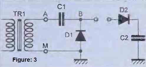
The first circuit presented here is an isolated case, it is the LATOUR voltage doubler described in figure 1.
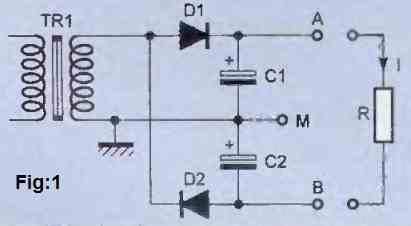
It allows obtaining a DC voltage of 2 x Vc between points A and B from an AC voltage source with an effective voltage Ve and a peak voltage Vc = 1.41 x Ve volts.
The interesting feature of this circuit is the presence of a center tap (M), which is very useful for operational amplifier circuits when the power transformer does not have this center tap in its construction.
The operating principle of the circuit is very simple: diode D1 rectifies the positive half cycles of the input voltage to charge capacitor C1, and diode D2 operates in the same way with the negative half cycles to charge capacitor C2.
The disadvantage of this method is that it generates a large ripple voltage when the circuit delivers a significant current. Typically, the peak-to-peak ripple voltage will be:
Uripple = (1.5/C) x I/F if C=C1=C2 and I is the current consumed by the load R in figure 1, and F is the frequency of the AC power supply. The actual output voltage will be Us = 2 x Vc - Uripple.
When measured with a multimeter, the reading will be Us = 2 x Vc - Uripple/2 because the multimeter will add the average of the ripple voltage.
Schenkel Voltage Doubler
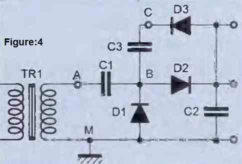
The second circuit serves as the basis for all the voltage multiplier circuits that we will see later. It is the Schenkel voltage doubler described in figure 2.
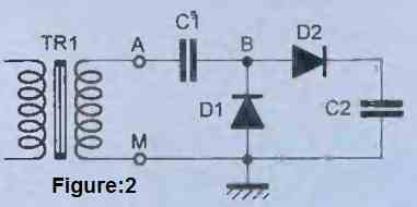
As in the previous example, if the peak amplitude of the AC voltage from the transformer is Vc, then we will obtain a DC voltage of approximately 2 x Vc across C2, but only under no load conditions.
To understand the operation of this circuit, it is necessary to separate it into two sub-assemblies, as shown in figure 3, in order to distinguish their respective roles.
The purpose of the first sub-assembly C1/D1 is to shift the starting AC voltage by a constant voltage so as to increase the peak value of the potential variation seen at point B.
We know that the potential at point A varies from +Vc for the positive half cycles to -Vc for the negative half cycles relative to the ground point marked M.
If the capacitor C1 is initially discharged, the potential at point B will follow that at point A for the first positive half cycle (ignoring the influence of D2 and C2), but its potential cannot drop below that of the ground point due to the presence of D1.
As a result, when the potential at A reaches -Vc during the negative half cycles, capacitor C1 will charge up to the voltage VB-VA=Vc.
Then, during the rise of the potential at A, the capacitor will not discharge (still considering C1/D1 as isolated), and the potential at B will follow this rise plus the voltage Vc across C1, thus creating the desired shift.
In this way, when the potential at A reaches the positive peak potential of +Vc, the potential at point B reaches the peak potential of Vc+Vc=2 x Vc, which corresponds to the doubling of the original peak voltage.
Then, all that is necessary is to add the second sub-assembly consisting of C2/D2 configured as a peak detector to obtain a DC voltage of Us=2 x Vc across C2.
However, the doubler is never used unloaded and it is interesting to have an idea of the ripple and the available holding voltage at the output as a function of the consumed current.
The following formulas attempt to achieve this, which are only approximations obtained by considering the charging time of capacitor C2 as negligible compared to its discharge time, but they remain indicative over a wide range of use as long as the doubler is not completely overloaded.
The ripple is given by: Uripple = 1/(F x C2), where F is the frequency of the voltage generator and 1 is the current consumed by the circuit.
The output voltage is given by: Us = 2 x Vc - (1 + C2/C1) x Uripple.
For example, in case where the transformer TR1 is a 12 Veff model (which gives Vc=1.41 x 12=17V) with F=50 Hz, C1=1 uF, C2=3.3 uF, and with a current consumed of 1=400 uA, we will have Uripple=2.4 V and Us=2 x 17-(1+3.3) x 2.4=23.6 V approximately, instead of 34 V unloaded.
If we take C1=0.47 uF, then Uripple will remain unchanged but we will have Us=2 x 17-(1+7) x 2.4=14.8 V only, which is less than the voltage obtained at the output of a classical bridge rectifier.
Now, with a 48 Veff transformer, therefore with Vc=1.41 x 48 V=68 V while keeping all other parameters the same:
Uripple does not change, and the second formula gives Us=2 x 67.7-(1+7) x 2.4=116 V approximately.
This time, however, the voltage is much higher than that provided by a bridge rectifier. We notice that the doubler gains in efficiency with an increase in the voltage to be doubled.
In the real case, a few other parameters will still affect this result: the threshold of the diodes slightly decreases the available voltage at the output.
During the measurements, simply connecting a multimeter can affect the result due to the consumed current if the capacitor values are low and the frequency of the low-voltage source.
Additionally, the calculated voltage Us does not take into account the average value of the ripple; the value read on the voltmeter will be rather close to Us+1/2 x Uripple.
Finally, since the consumed current is often low, the available voltage at the output of transformer TR1 will be higher by 10 to 20% of its announced service voltage and will contribute to increasing the available voltage at the output of the doubler.
To improve the load performance of the circuit, one may be tempted to choose a polarized model with high capacitance for C1.
However, it should be noted that at startup, if the first positive half-wave occurs while C1 is still discharged, it will be charged in reverse voltage through D2 and C2 before finding its normal operating regime during the following negative half-wave. It is possible that it can withstand it, but the risk exists.
Therefore, to use high values for C1 safely, non-polarized electrochemical models should be used.
Greinacher Cascade
The major advantage of the Schenkel doubler is the possibility of connecting any number "n" of them in a row to obtain an output voltage of value 2 x n times the peak value of the input AC voltage. It is then called a Greinacher cascade.
For more gain, an example of assembling two successive doublers is described step by step in figures 4, 5, and 6.
The first step (figure 4) consists of adding to the circuit of figure 2 (assembly D3/C3, similar to C1/D1, intended to shift the positive peak potential present at point B by a DC voltage of 2 x Vc).
Indeed, the potential of B varies, as we have seen, between 0 V and 2 x Vc, and the potential of point C cannot drop below 2 x Vc, which is the voltage across C2 due to diode D3.
Therefore, during the negative half-cycles of the input voltage, capacitor C3 will charge with a voltage of 2 x Vc.
With the rise of this voltage, the potential of C will follow the variations of B, shifted by this value of 2 x Vc, and when the potential of point B finally reaches 2 x Vc, point C will reach the peak potential of 4 x Vc.
It is then sufficient to add, as shown in figure 5, the peak detector D4/C4 to obtain the rectified voltage of 4 x Vc across C4.
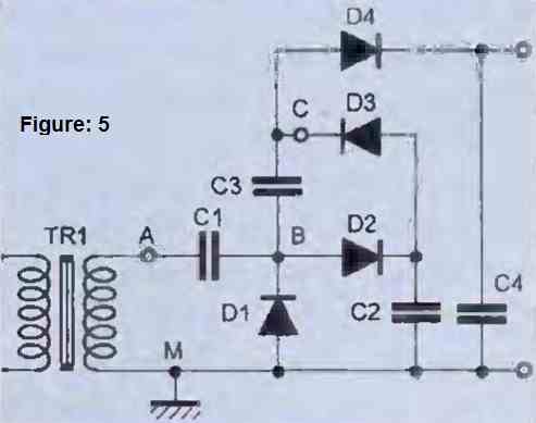
However, it can be noticed that capacitor C4 must have a rated voltage of 4 x Vc, which can become difficult and expensive when trying to achieve high voltage levels.
Therefore, it is more advisable to connect the second electrode of C4 not to the ground, but to the common point between D2 and C2, which is already at a potential of 2 x Vc, as seen in figure 6.
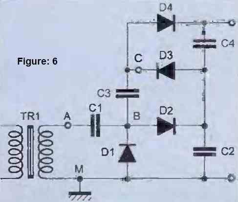
This way, the rated voltage of C4 does not have to exceed 2 x Vc.
If a new doubler element is added, as in figure 7, the results obtained are generalized: each doubler element added (here C5/D5/C6/D6) shifts the peak voltage by 2 x Vc, and one obtains a rectified voltage between point E and ground of around 6 x Vc (n=3 doublers), regardless of the number of doublers "n" in the chain and the final voltage obtained.
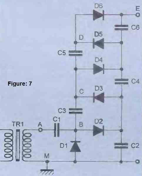
Each capacitor should have a rated voltage of 2 x Vc, and the diodes should be able to withstand a reverse voltage of slightly more than 2 x Vc as well.
Thus, it can be seen that one can obtain an output voltage of 2 x n x Vc without any component being designed to withstand such a voltage, which is yet another interesting property of these assemblies.
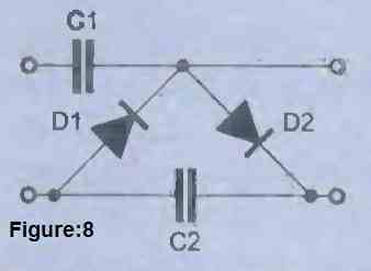
Figure 8 shows the classic representation of a doubler element in a chain, which can be easily compared to figure 2.
This type of assembly is used, for example, to generate the high voltages required for the operation of particle accelerators, and these generators are then called Cockcroft-Walton generators.
Estimating the available output voltage of these doubler chains when the assembly provides a current I is more complicated.
In the case of the multiplier in figure 6, for example, if C1 is indeed charged to the voltage Vc, C3 should only be charged to the voltage U=2 x Vc-(1+C2/C1) x 1/(F x C2), which is already less than 2 x Vc.
However, C3 actually discharges C2 during this charging process and thus decreases the maximum voltage at its terminals, of which C4 will only benefit partially due to the discharge of C3 during its own recharge.
The efficiency decreases from stage to stage while the ripple continues to increase due to these cross-charging and discharging. For example, in the case of the multiplier in Figure 6 with values of C1=C3=0.47 uF, C2=C4=3.3 uF, F=50 Hz, and Vc=17 V, we will have a voltage of Us=68 V when there is no load (1=0).
Under a current of 50 pA, we will still have Us=56 V, but for a current of 400 pA, the output voltage Us will be only 19 V.
In fact, if one sizes the component values such that a single doubler element maintains its optimal output voltage under the desired current I (which can be verified using the formulas from the previous paragraph), then it is highly likely that cascading several identical elements will also give the desired result, which is the simplest way to determine the correct values.
Multiplication by odd numbers:
The case of the triple multiplier In the case of the triple multiplier (Figure 9), the double multiplier element D1/C1/D2/C2 is connected after a peak rectifier consisting of D0/C0.
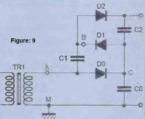
Thus, the potential at point C is fixed at Vc and the potential at point B, due to the presence of the C1/D1 combination, will fluctuate between Vc and 3 x Vc since C1 will charge to a voltage of 2 x Vc during the negative half-cycles of the input voltage.
Thus, at the output of the peak detector D2/C2, we will find the rectified voltage 3 x Vc, resulting in a tripling of the original voltage.
If C0 is chosen to be significantly larger than C1, the formulas for the double multiplier can be used and we have:
Uond=(1/C0+1/C2) x I/F for a consumed current I, and also:
Us=3 x Vc-3 x I/(2 x F x C0)-(1+C2/C1) xI/(FxC2).
The corrective term -3 x 1/(2 x F x C0) comes from the influence of the voltage ripple across C3 on the overall voltage and on the charge of C1, but this term is often negligible.
As before, additional double multiplier elements can be added to obtain voltages of 5 x Ve, 7 x Ve, etc.
Converting DC/DC is entirely possible using such multipliers to generate high DC voltages from lower DC voltages.
Using an Op Amp
The first example is shown in Figure 10 using an oscillator built around an operational amplifier generating a square wave of any frequency, but preferably high enough to reduce the value of capacitors in the doubler chain.
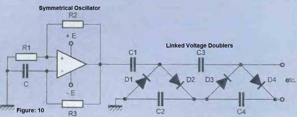
All the teeth and formulas mentioned earlier are valid by taking Vc=E for a rail-to-rail amplifier, otherwise, it will be slightly less.
Using IC 555
This is not the case in this second example where a simple oscillator (Figure 11) is used, whose output voltage oscillates between 0 and Vcc, that is, in a non-symmetrical way with respect to the ground.
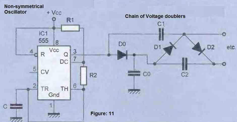
It is evident that if one connects a doubler similar to that of Figure 2 to this circuit, capacitor C1 will never charge adequately, and only odd multiplier circuits such as triplets and odd multipliers will be usable.
However, in this case, the formula will be different: the voltage obtained at the output of the tripled circuit will be: Us = Vcc + 2 x (Vcc / 2) and in the case of a cascade of "n" elements derived from the tripled circuit: Us = Vcc + 2 x n x (Vcc / 2). That is, Us = (n+1) x Vcc.
Assuming that the output signal of the amplifier is symmetrical with respect to the ground, this oscillator perfectly substitutes the transformer of the previous examples.
Summarizing
The electronic circuit device which is used for stepping up voltage to a 2x order by charging capacitors from a lower input voltage is known as voltage doubler.
The charge current is switched in such a manner that in any ideal situation, the voltage which is produced at the output is exactly two times that of the voltage at input.
Simplest Voltage Multiplier using Diodes
The simplest form of the voltage doubler circuit are a type of rectifier which takes the input in the form of Alternate Current (AC) voltage and produces a double magnitude of (DC) voltage as the output.
Simple diodes are used as switching elements and an input in the form of mere alternating voltage is used to drive these diodes in a switching state.
An additional driving circuit is required in order to control the switching rate in case voltage doublers being used are of DC to DC type since they cannot be switched in the above manner.
The DC to DC voltage converter circuits most of the times require another additional device called switching element which can be easily and directly controlled such as in a transistor.
Thus, when it uses switching element, it does not have to depend on the voltage present across the switch as is the case in a simple form of AC to DC.
The voltage doubler is a type of the voltage multiplier circuit. Most of the voltage doubler circuits with few exceptions can be viewed in the form of a higher order multiplier at a single stage. Also, a greater amount of voltage multiplication is achieved when there are cascading identical stages which are being used together.
Villard Circuit
The Villard circuit has a simple composition consisting of a diode and a capacitor. On the one hand where the Villard circuit provides benefit in terms of simplicity, on the other hand it is also known to produce output which has ripple characteristics which are considered very poor.
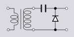
Figure 1.Villard circuit
Essentially, the Villard circuit is a form of diode clamp circuit. The negative high cycles are used in order to charge the capacitor to the AC peak voltage (Vpk). The AC waveform as the input along with the capacitor’s steady DC’s superposition forms the output.
The waveform’s DC value is shifted by using the effect of the circuit on it. Since the diode clamps the AC waveform’s negative peaks to the value of 0V (in actual terms it is –VF, which is the small forward bias voltage of the diode); the output waveform’s positive peaks are of the value of 2Vpk.
The peak-to-peak is difficult to smoothen since it is of enormous size of the value of 2Vpk and thus it can be smoothed only when the circuit is transformed into any other more sophisticated forms in an effective manner.
The negative high voltage is supplied to the magnetron by using this circuit (which consists of diode in reverse form) in a microwave oven.
Greinacher circuit
The Greinarcher voltage doubler has proved to be better than the Villard circuit by improving itself significantly by adding some additional components for a small cost.
Under the condition of open-circuit load the ripple is found to be reduced very much, most of the times to a state of zero; but the resistance of the load and the value of the capacitor which is being used play an important role and affect the current being drawn.
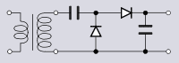
Figure 2. Greinacher circuit
The Villard cell stage is followed by the circuit in order to work by using an envelope detector stage or a peak detector.
The effect of the peak detector is such that much of the ripple is removed while the output of the peak voltage is preserved as such.
Heinrich Greinacher was the first person to invent this circuit in 1913 (which was published in 1914) in order to provide the voltage of 200-300V which was needed by him for his ionometer which was again a new invention by him.
The requirement of inventing this circuit to get that much voltage arose because the power supplied by the Zurich power stations was of only 110V AC and thus was insufficient.
Heinrich developed this idea more in 1920 and extended it to make a cascade of multipliers. Most of the times, people refer this cascade of multipliers invented by Heinrich Greinacher as a Villard cascade which is inaccurate and not true.
This cascade of multipliers is also known as Cockroft-Walton after the scientists John Cockroft and Ernest Walton who had built the particle accelerator machine and had rediscovered the circuit independently in 1932.
The use of two Greinacher cells which have polarities opposite to each other but being driven from the same AC source can extend the concept of this kind of topology to a voltage quadrupler circuit.
The two individual outputs are used in order to take down the output across them. The grounding of the input and output simultaneously in this circuit is quite impossible as is the case with a bridge circuit.
Bridge Circuit
The kind of topology used by a Delon circuit in order to have voltage doubling is known as bridge topology.
One of the common uses of this type of delon circuit was found to be in the television sets with cathode ray tube. The delon circuit in these television sets was used in order to provide the e.h.t. voltage supply.
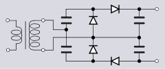
Figure 3.Voltage quadrupler – two Greinacher cells of opposite polarities
There are many safety hazards and issues associated with the generation of voltages of more than 5kV along with being highly uneconomic in a transformer mostly in the equipment which are domestic equipment.
But an e.h.t. of 10kV is a basic requirement of the television sets which are black and white while the colour television sets require even more e.h.t.
There are different ways and means by which the e.h.t. of such dimensions are achieved such as: doubling the voltage on the mains transformer within an e.h.t winding on it by using voltage doublers; or by applying the voltage doublers to the waveform on the line flyback coils.
The two peak detectors consisting of half-wave within a circuit are functionally similar to the peak detector cells found in the Greinacher circuit.
The half-cycles which are opposite to each other of the incoming waveform are used for operating by each of the two peak detector cells. The output is always found to be double of the peak input voltage since the outputs produced by them are in series.
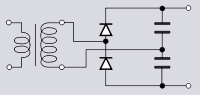
Figure 4. Bridge (Delon) voltage doubler
Switched Capacitor Circuits
The voltage of a DC source can be doubled by using the diode-capacitor circuits which are simple enough and have been described in the above section by preceding the voltage doubler with the use of a chopper circuit.
Thus, this is effective in converting the DC to AC before it goes through the voltage doubler. In order to attain and built circuits which are more efficient, the switching devices are driven from an external clock which is proficient in functioning both in terms of chopping and multiplying and can be achieved on a simultaneous basis.
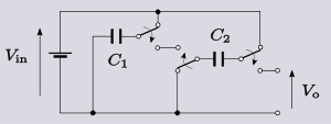
Figure 5.
Switched capacitor voltage doubler achieved by simply switching charged capacitors from parallel to seriesThese types of circuits are known as switched capacitor circuits.
The applications which are powered by low voltage are the applications which especially use this approach since integrated circuits have a requirement of a supply of specific amount of voltage which is more than what the battery can actually deliver or produce.
In most of the cases, there is always an availability of a clock signal on board of the integrated circuit and thus this makes it unnecessary to have any other additional circuitry or only little circuitry is needed to generate it.
Thus, the diagram in Figure 5 displays schematically the simplest form of switched capacitor configuration. In this diagram, there are two capacitors which have been charged to the same voltage simultaneously in a parallel.
Post this; capacitors are switched into series after switching off the supply. Thus, the output voltage produced is twice the supply or input voltage in case the output is derived from the two capacitors in series.
There are various different kinds of switching devices which can be used in such circuits, but MOSFET devices are the most frequently used switching devices in the case of integrated circuits.
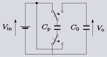
Figure 6. Charge-pump voltage doubler schematic
The diagram in Figure 6 displays schematically one of the other basic concepts of the “Charge Pump”. The input voltage is used to first charge the Cp, the charge pump capacitor.
After this, the output capacitor, C0 is charged by switching in series with the input voltage which results in charging the C0 double the amount of input voltage. In order to successfully charge C0 fully, the charge pump may be required to take many cycles.
But once a steady state has been acquired, the only essential thing for the charge pump capacitor, Cp is to pump charge in small amounts which is equivalent to the charge being supplied from the output capacitor, C0 to the load.
A ripple is formed on the output voltage when C0 gets discharged partially into the load while it is being disconnected from the charge pump. This ripple formed in this process has the characteristic of shorter discharge time and easy to be filtered and thus these characteristics make them smaller for frequencies for higher clock frequencies.
Thus, for any given specific ripple, the capacitors can be made smaller. The maximum amount of clock frequency for all practical purposes in the integrated circuits typically falls in the range of hundreds of kHz.
Dickson charge pump
The Dickson charge pump, also known as Dickson multiplier consists of a cascade of diode/capacitor cells where a clock pulse train drives the bottom plate of each of the capacitor.
The circuit is considered to be a modification of the Cockcroft-Walton multiplier but with the only exception of switching signal being provided by the DC input with clock trains instead of an AC input as is the case with Cockcroft-Walton multiplier.
The basic requirement of a Dickson multiplier is that the clock pulses of phases opposite to each other should drive the alternate cells. But, in the case of a voltage doubler, depicted in the Figure 7, only a single clock signal is required since there is only one stage of multiplication.
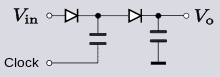
Figure 7. Dickson charge-pump voltage-doubler
The circuits where Dickson multipliers are mostly and frequently used are the integrated circuits where the supply voltage such as from any battery is less than what is required by the circuitry.
The fact that all the semiconductors used in this are basically similar acts as an advantage for the manufacturers of the integrated circuit.
The standard logic block which is most commonly found and used in numerous integrated circuits is the MOSFET devices.
This is one of the reasons why the diodes are many a times replaced by the transistor of this type, but are also wired to a function in the form of a diode.
This arrangement is also known as a diode-wired MOSFET. The diagram in Figure 8 depicts a Dickson voltage doubler using this kind of diode-wired n-channel enhancement type MOSFET devices.
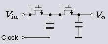
Figure 8. Dickson voltage doubler using diode-wired MOSFETs
The basic form of Dickson charge pump has undergone a lot many improvements and variations. Most of these improvements are in the area of the reduction of the effect produced by the transistor drain source voltage. This improvement is considered as significant in case the input voltage is small as is in the case of a low-voltage battery.
The output voltage is always an integral multiple of the input voltage (twice in case of a voltage doubler) when ideal switching elements are used.
But in case where a single-cell battery is used as the input source along with MOSFET switches, the output in such cases are far lesser than this value because there will a drop in the voltage across the transistors.
Due to the extremely low drop in the voltage in the on-state of a circuit which is using discrete components, the Schottky diode is considered a good choice as a switching element.
But the designers of integrated circuit mostly prefer MOSFET to use as it is more easily available which more than compensate for the presence of inadequacies and high complexity in the circuit which is present in MOSFET devices.
To illustrate this, let us take an example: a nominal voltage of the tune of 1.5V is present in an alkaline battery.
The output in this can be doubled to 3.0V by using a voltage doubler along with ideal switching elements which has a voltage drop of zero.
But the diode-wired MOSFET’s voltage drop of drain-source when it is in the state of on must be at the minimum equal to the gate threshold voltage which is typically in the tune of 0.9V.
The output voltage can be raised by the voltage doubler successfully only by approximately 0.6V to 2.1V.
The increase in the voltage by the circuit cannot be achieved without using multiple stages in case the drop across the final smoothing transistor is also considered and taken into account.
On the other hand, the onstage voltage of a typical Schottky diode is of 0.3 V. the output voltage produced by a voltage doubler will be in the range of 2.7V if it uses Schottky diode, or 2.4V if it uses smoothing diode.
Cross-coupled switched capacitors
The cross-coupled switched capacitor circuits are known for the input voltage being very low. A single-celled battery can be required in the equipments which are driven by wireless battery such as pagers and Bluetooth devices in order to supply power continuously when it has discharged to under a volt.
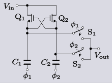
Figure 9. Cross-coupled switched-capacitor voltage doubler
The transistor Q2 is turned off in case the clock is low. At the same time, the transistor Q1 is turned on if the clock is high and this results in the charging of the capacitor C1 to the voltage Vn. the top plate of C1 is pushed up to double Vin in case the Ø1 goes high.
In order to enable this voltage to appear as an output, the switch S1 closes at the same time. Also, at the same time C2 is allowed to charge by turning on the Q2.
The roles of the components are reversed in the next half cycle: Ø1 will be low, S1 will open, Ø2 will be high, and S2 will close.
Thus alternatively from each side of the circuit, the output voltage is supplied with 2Vin. the loss incurred in this circuit is low since there is a lack of diode-wired MOSFETs and the threshold voltage problems associated with it.
One of the other advantages of the circuit is that it doubles the ripple frequency since there are two voltage doublers present which supply the output effectively from the phase clocks.
The basic disadvantage of this circuit is that the stray capacitances of the Dickinson multiplier is found to be much less significant than this circuit and thus accounts for the most of the losses which are incurred in this circuit.
Courtesy: https://en.wikipedia.org/wiki/Voltage_doubler

Questions & Answers
Hello,
I’m interested in the Villiard circuit because this is the same circuit used for level shifting the primary voltage on my vacuum tube Tesla coil. Can you tell me how to calculate the capacitance value? My plate transformer is 1500 v rms and around 400 miliamps. I imagine it would be something like voltage out = current/impedance. I’m using a 1.05 μF microwave capacitor but I think it needs 2 more capacitors in parallel.
Hi, for calculating the current output from the capacitor, you can implement the steps explaied under the following article:
https://www.homemade-circuits.com/how-to-calculate-and-deduce-current-and/
Please read under the section:
Finding Capacitor Current
Let me know if you have any further doubts…
Hello Mr swagatam,
have you ever applied the cross coupled charge pump in the cadence,
during the first cycle when pi1=0v and hence pi2= vdd, how upper plate capacitor gets vdd voltage ?
Hello Parm, i am not yet familiar with cross coupled charge pump in cadence. If possible I will try to investigate it.
Hello Swagatam, first off thanks for all the cool circuits, I look forward to everyone you send out. Ok, I have a 200 volt 3 amp switch mode power supply. I would like to make it variable and variable current if possible. Are the any circuits you have in your database that could help ne out. I see lots of tfe fir the lower voltages. Thank your time in this matter.
ART
Thank you art, you can refer to the following article for getting all the required info: Please check out the last diagram for easy understanding:
https://www.homemade-circuits.com/how-to-make-variable-current-smps/
halo mR swagatan i m in australia just a qouestion how much do you know about time machins ; and steven gibbs; im un inventor & a few years ego i inented the multy tap hf antenna which you mite know i will apretietif you replay on that i follow you on internet but iwas sick to have a comunnication with you
Hello Sir, please I read how 24v/10amps was converted to 10v/24amps using charge pump, how can I convert my trafo with 30V/2amps to be like charge pump as above in possible to 4amps
Hello Tinu, charge pump cannot be used to produce a bucked output, with boosted current. You will need a buck converter for that. You can try the following circuit for fulfilling your requirement:
https://www.homemade-circuits.com/0-to-50-v-adjustable-switching-power-supply-circuit-using-ic-lm2576/
Hello eleftherio, the only thing that I know about time machine is that they exist only in books, they are not feasible in real life.