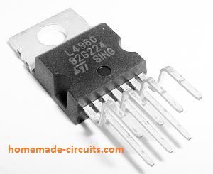
The explained variable switching power supply circuit is designed around the integrated switch mode power supply controller device Type L4960 from SGS. The main features of this switching regulator can be summarized from the following data:
Main Features
- Input voltage range: 9-50 VDC
- Output voltage variable from 5 to 40 V.
- Maximum accessible output current is: 2.5 Amps.
- Highest possible output power is: 100 Watts.
- Integrated soft-start circuitry.
- Stabilized internal reference level with ±4% margin
- Works with handful of external parts.
- Duty factor: 0-1.
- High efficiency, having η up to 90%.
- Has an internal thermal overload protection.
- Includes an internal current limiter which ensures complete shortcircuit protection.
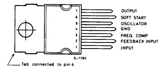
The pin specifications of the chip is shown in the following figure. The L4964 is encased within a exclusive 15-pin package, designed to handle up to 4 A.
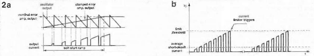
The working of the in-built soft start circuitry, and the current limiter, is highlighted through the below shown waveform drawings, respectively.
The over temperature shut off circuit in the L4960 is triggered as soon as the IC case temperature goes higher than 125 °C. For safety concerns , the suggested switch mode power supply circuit is recommended with transformer based layout.
The AC input voltage to the PCB is acquired from the mains transformer secondary winding, which means that the DC to the IC is at minimum 3 V above the necessary output voltage with the highest possible output current. It's understandable that the transformer is essentially a toroidal model.
Circuit description
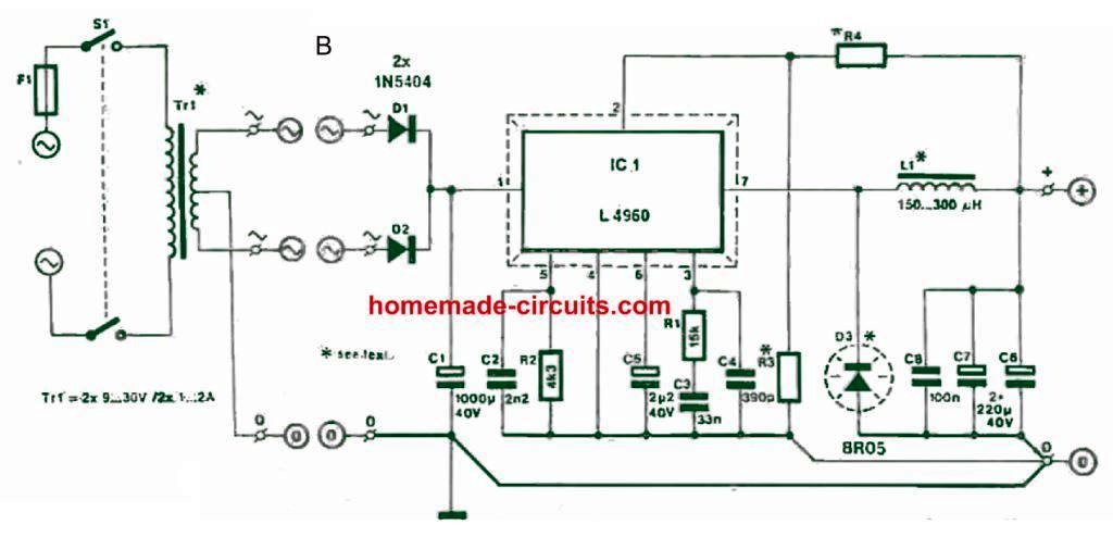
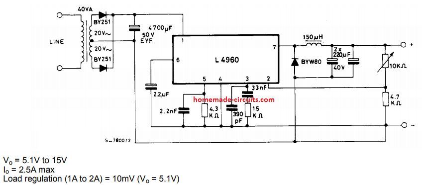
The circuit diagrams above exhibit the mains transformer AC section design, and the DC switching power supply, correspondingly. The AC voltage from the secondary side is goes to the individual inputs over the supply board, while the center tap is hooked up to ground line.
The unregulated input voltage, Ui for the IC comes through a full-wave rectifier circuit made up of a pair of 3 A diodes 1N5404, D1-D2, along with a filter capacitor, Ct. Circuit consisting of R1-C3-C4 highlights the closed regulation loop gain. Another circuit stage using C2 -R2, is configured to generate oscillator frequency of approximately 100 kHz.
The C5 capacitor C5 actually has two functions: this specifies the time of the soft start ramp as shown in the above waveform image, and also the average short-circuit current. The feedback input of the L4962 is coupled to the output voltage divider R3 -R4 junction. The output voltage, Uo, of the L4960 is determined using the following calculations
Uo =5.1[(R 3 + R4)/R3] given that Ui - Uo ≥ 3 V.
Note that the lowest value of Ui has to be 9 V. we are able to get a fixed output voltage of 5.1 V (±4%) as soon as R3 is removed, and R4 changed with a short link. If R3 is selected with a fixed value of 5K6, R4 individually decides the output voltage:
Uo =9 V: R4 = 4K3
Uo =12 V: R4 = 7K6
Uo =15 V: R4 = 10K
Uo =18 V: R4 = 14K
Uo =24 V: R4 = 20K
The design can be converted a variable switch mode power supply by using R3 = 6K8 and upgrading R3 with a 25K potentiometer. Diode D3 is incorporated for protection of the IC. This fast rectifier restricts the negative spikes at the inductor input side to a harmless 0.6 to 1 V for every switch off periods of the ICs internal output transistor.
If D3 was not there it would cause pin 7 potential of the IC to rise hazardously to many volts below the ground potential. Inductor L1 along with the diode D3 and the capacitor C6 C7, acts like a buck converter for regulating the output in a switched mode, thereby causing much lower heat dissipation compared any other linear IC circuit such as LM338.
Construction
The compact PCB track and component layout can be visualized in the following image.
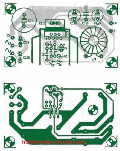
Assembling the board is actually very easy. Begin by choosing resistors R3 and R4 as previously mentioned. First assemble the parts that are around the center of the pcb like the, R1… R4 inclusive as well as C2 C5.
Before you start soldering the parts, make sure that the regulator IC1 and power diode D1 are clamped through screw/nut back to back over a single common heatsink as proven on the image of the component overlay.
Do remember to maintain the heatsink electrically well insulated from the IC metal tab using a thicker mica washer and a plastic material bush. You possibly can make use of the Type BYV28 for the diode D3.. Whichever diode type is selected, make sure that the mic insulation with a continuity tester!
Press the ICI and D3 pins into their particular PCB holes right up until the heatsink beds down firmly over the PCB surface. Now, solder the leads and cut off their remaining unwanted portion of the lleads. After this, install the rest of the parts, L1, CI, C6, C7, Cs, D1 and D2.
Make sure to watch diode and the electrolytic capacitors pin orientation and polarity correctly. Excessive attention must be exercised to prevent any kind of chance of a short-circuit across choke core winding with the IC heatsink. It is advised to secure L1 using a central nylon bolt and nut assembly.
Testing and Efficiency
Begin the testing procedure by checking the placement, insulation and direction of each and every components on the PCB before you connect the board to the transformer secondary side wires.
It must be noted that this adjustable switching power supply needs a load connected at the output constantly in order to work optimally. When the SMPS is supplied with 30 VAC, and a 2 A load attached to an output voltage of 5 V, the heatsink temperature must not exceed around 60 °C at room temperature.
The efficiency of the circuit under such circumstances can be expected to be around 68%. The efficiency boosts to 80% when Uo=10 V, 85% at Uo =15 V, to 87% at at Uo=25 V, all with load rated at 2 Amps.


Questions & Answers
Hi! what happens if you disconnect the load? does the output voltage increases to the input voltage value or this ic have a protection against this? if doesn’t, will it damage the ic?
Hi, due to the feedback loop at pin#2 of the IC, the output voltage should remain constant regardless of whether a load is connected or not.
Thank you!!! I’m testing this circuit now and everything works fine but only when the input voltage is less than 16V. If the input voltage is higher than 16V, the output voltage drops to 2V or even less. Do you have any idea of why is this happening?
The above circuit is designed to work with input voltages upto 50 V DC, so I am not sure why your are facing this problem??
Please check all the connections and part values correctly and test again.
The problem was that I didn’t put the input capacitor, I thought it was just for filtering so I omitted it for the test. I don’t know what its function is, but now it works, I’m so confused hahaha.
Thanks!!!
Yes the input capacitor after the rectifier diodes is for filtration. No problem, glad it is working now!
Ok..
Iam looking a voltage regulator circuit only few componen.
Input 1-5 volt from pararel source (solarcell+recharge battery or other)
Variable Output
0- 5 volt
0-200microamp
Thanks
You can try the first circuit from this article:
https://www.homemade-circuits.com/low-dropout-5v-12v-regulator-circuits-using-transistors/
Replace the zener diode with a 1k resistor and replace the 1k5 resistor with a 10k pot. You can also replace Q1, Q2 with BC557, BC547 respectively.
hi mr swag .. I am working on a pulse motor project, until now I archieve a power consume of 3.7mikrowatt from 1.5V and 2.5mikroamp. I need several components in voltage regulator so that the voltage can be constant 0.1-5 volts from the varied input. Can you help me? I can not sent picture or video in here yeay?
Mpiq, your question is not clear, please explain the specifications and requirements correctly
Dear Swagatam
I am looking for variable power Supply circuit which can deliver 60 volt , 100 amps DC for induction heating as a power supply source.
Thanks
Dear Samant, since the current is very high, a transformer based power supply will be more suitable. More simply a 30 amp varaic is what I would recommend.
I love this design but for testing high power amplifiers I need much more power, say – dual adjustable 150Vdc @ 50A, can you provide such a detailed design?
I appreciate your feedback
However, I do not have the 150V 50 amp control circuit at this moment, if I happen to find the circuit, will post it for you in this website.
Thank you, I’ll appreciate it.