In this post I have explained how to make a simple variable power supply circuit using transistor 2N3055 and some other passive components. It includes variable voltage and variable current feature, fully adjustable.
Main Specifications
1) Adjustable from 0-30V, 0-60V, and 0-100V, and 500mA to 10 Amp as per user preference
2) Short Circuit Protected when mounted on proper heatsink
3) Ripple free, with less than 1Vpp
4) Output is Stabilized and filtered DC
5) Short circuit LED indicator
6) Overload Protected
Introduction
A power supply circuit that does not include the features of a variable voltage and current control can by no means be considered truly versatile.
A variable workbench power supply circuit I have explained in this article is not only specified with a continuously variable voltage control but is also equipped with the feature of overload or continuously variable current control.
Circuit Diagram
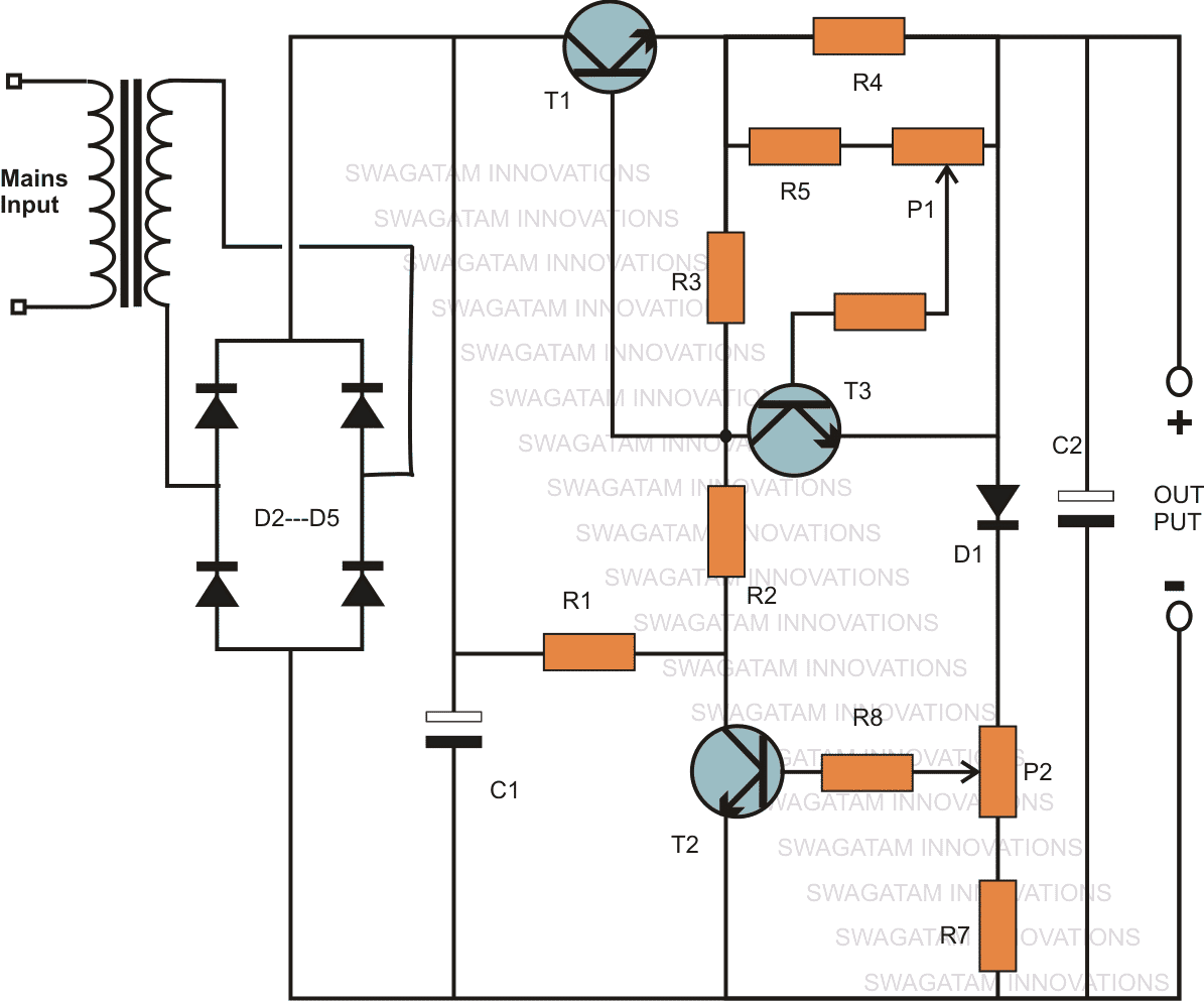
How it Works
A keen look at this 2N3055 based variable voltage current power supply circuit using transistor 2N3055 reveals that it’s actually only an ordinary stabilized power supply circuit, however it yet still provides you with the proposed features very efficiently.The voltage variations are made by using the preset P2, through a feedback configuration employing the components D1, R7, T2 and P2.
The inclusion of D1 makes it sure that the voltage can be lowered right down to 0.6 volts, which happens to be the forward voltage drop of the diode.
If any other specific minimum value is required then the diode can be replaced by zener diode having the required specified value.
Therefore in this variable power supply circuit using 2N3055 transistor, the transformer being a 0 – 40 V, the output becomes variable right from 0.6 to 40 volts maximum, that’s very handy indeed.
For implementing the current control feature, T3 along with P1, R5 and R4 are involved.
The value of R4 is specifically becomes responsible for defining the maximum allowable output current.
P1 is set to choose the maximum range within the value that’s marked or identified by the resistor R4.
PCB Design
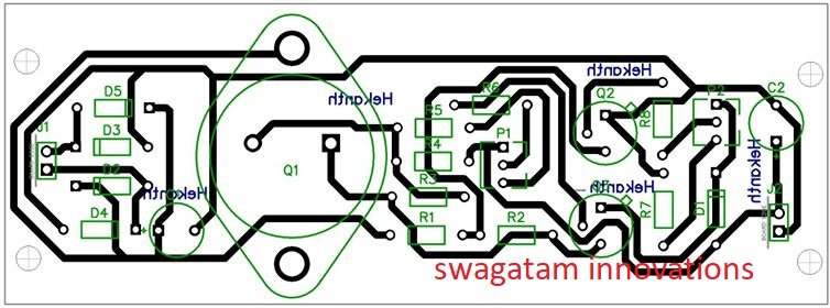
Parts List
- R1 = 1K, 5 watt wire wound
- R2 = 120 Ohms,
- R3 = 330 Ohms,
- R4 = to be calculated using Ohms law.
- R5 = 1K5,
- R6 = 5K6,
- R7 = 56 Ohms,
- R8 = 2K2, P1,P2 = 2k5 presets
- T1 = 2N3055,
- T2, T3 = BC547B,
- D1 = 1N4007,
- D2, D3, D4, D5 = 1N5402,
- C1, C2 = 1000uF/50V,
- Tr1 = 0 – 40 Volts, 3 Amp
2N3055 Pinout Details
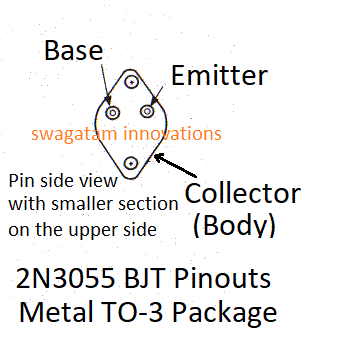
If you have any doubts regarding this variable voltage and current power supply circuit using transistor 2N3055 circuit please do not hesitate to ask then through the comments below.
Original Transistor Power Supply Diagram:
The above design was inspired from the following circuit which was designed and presented in the elektor electronics magazine by the elektor engineers:
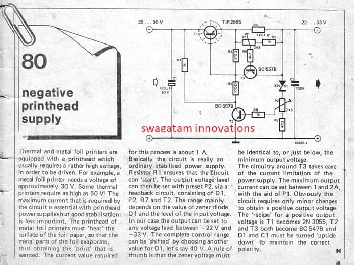
Simplified Variable Power Supply Design using 2N3055 and 2N2222 Transistors
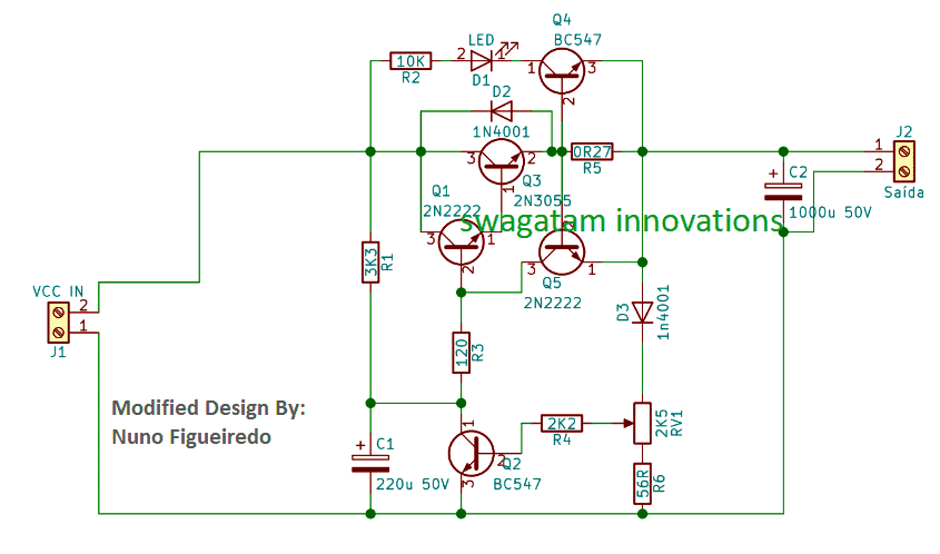
The above designs were assessed and simplified with more effective results by Mr. Nuno. The revised and simplified design can be viewed in the following diagram:
The design features an over-current shut down with LED indication.
Video clip of the tested prototype:
For PCB Design and other Related Data, you can Download the following ZIP File:
PCB Design for the above Circuit
Another Similar Power Supply Design as Referred by Mr. William C. Colvin is presented below for the viewer assessment:
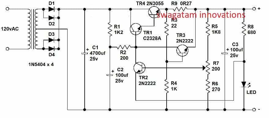
2N3055 Wide Range Variable Voltage Regulator
The key highlights of the circuit are: wide range output: 0.1 to 50 volts excellent load regulation: 0.005% between 0 and 1 amp, decent line regulation: 0.01%, reduced output disturbance: superior to 250 microvolts.
The broad output selection is implemented with thehelp of the integrated circuit CA 3130, that is able to work even with a zero volt input/output differential. In addition, higher extension of the output range becomes feasible through the inclusion of T4 between the IC and the series pass transistor.
The high gain as a result acquired enables a superior level of regulation, and the T1/T2 Darlington pair offers a adequately large current boosting. T3 works like an output current controller.
When P1 is rotated totally anti-clockwise, T3 restricts at 0.6 amps. The limiting circuit becomes inactive when P2 is moved completely clockwise. The regulator circuit specifically operates in the following manner.
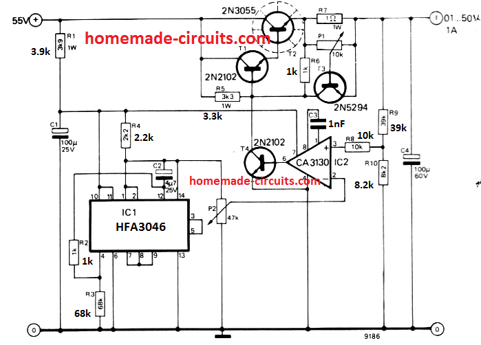
The IC CA 3130 analyzes the output voltage given to the non-inverting input with respect to a reference voltage at the inverting input.
The output voltage of the regulator is reduced with a potential divider to protect against damage to the IC.
The reference voltage is determined by P2, which needs to be a top-notch part, since any kind of noise upon its slider arm will probably be transferred to the regulator output terminals.
A additional IC, HFA3046 , offsets the reference voltage intended for temperature variations. The IC is made up of 4 transistors applied as diodes or zener and another transistor for cutting down the output impedance of the reference circuit.
The reference IC furthermore provides a stepped down supply voltage for powering CA 3130. This feature necessitates the use of each ICs in the regulator stage; if IC1 is removed can result in the break down of IC2. Each of the transistors shown in the diagram must be rated with a breakdown voltage of a minimum of 55 volts.
High Current Variable Power Supply
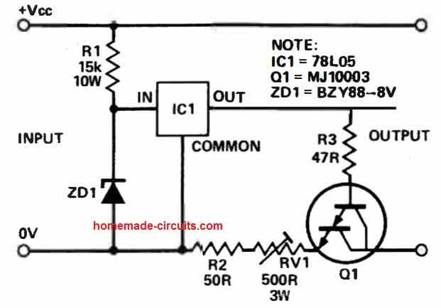
In this high current linear power supply circuit, we have used a 2N5686 transistor instead of 2N3055, so that the circuit is able to deliver a minimum of 10 amp current, and the preset P3 could be used to adjust a current range of 10 amp.
The power supply itself is pretty straightforward to construct. An IC LM329 provides a steady reference voltage of 6.9 V.
P4 is a potentiometer, and this pot is utilized to determine the output voltage using a preset potential divider P2-P4-R2. The power stage of the circuit is made up of IC1 and T1, which operate like an operational amplifier when it comes to positive voltages (negative voltages are not relevant here, obviously).
This non-inverting amplifier is built using an combo of op amp, P1, R5, and R6. This indicates that the voltage at P4's wiper is proportionate to the voltage across the output terminals.
P1 is a potentiometer that controls the peak output voltage, while P2 is used for setting the minimum output voltage from the power supply.
Preset P3 is used for setting up the maximum current limit of the output.
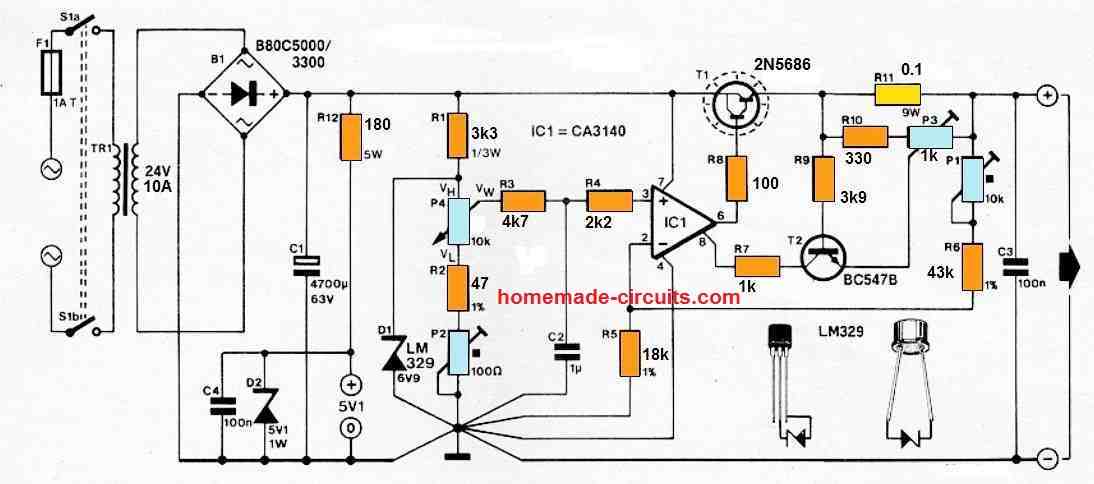
R11 converts the output current to a voltage to accomplish this. When this voltage (controlled by P3) is large enough to turn on T2, the circuit's voltage regulation is superseded by current regulation through IC1's strobe input. The maximum current that can be adjusted is from 0.8 A to 10 A, depending on how the controls are adjusted.
When the output of the power supply are short-circuited, the current must not increase above 25 A to prevent T1 from being damaged and due to over dissipation. The circuit setting up is not complicated. To begin, adjust P4 to highest possible resistance and wait about a minute until Z1 and IC1 reach their typical working temperatures. Next, adjust P1 to get a 25 V output voltage.
Finally, tweak P2 to provide a 250 mV output voltage by setting P4 to lowest resistance. The lowest output voltage of 250 mV was selected on purpose to guarantee that the individual parts always are able to work with a linear region of their characteristics. There are a couple of things to remember here: the earth lines must be routed exactly as shown in the schematic, and T1 must be installed on a 1.5 K/ W heat sink.


Questions & Answers
use the scan that is below first scan it is cleaned up better I used photo paper which allows scraping ink from pathways after printing with laser printer because i erased text from image there seems to be artifacts of it still showing up in traces so it still needs to be examined before final transfer to pcb.
Thanks very much mike, it is nicely done, I hope the readers will find it very helpful…
also filled Scan2025-02-20_233920.pdf
Thanks very much Mike, I extracted the image from the pdf, here it is:
https://www.homemade-circuits.com/wp-content/uploads/2025/02/pcb-scan_page-0002.jpg
i am trying to send image again dont see it and trying again
The above image is not clear, but your pdf image is very good, so I have extracted it and processed it as below:
https://www.homemade-circuits.com/wp-content/uploads/2025/02/pcb-scan_page-0002.jpg
I hope converting the pdf file to zip file is good enough smaller” I did have to take a sharp object to my toner transfer sheet printed out pcb and open up pathways before transfer to pcb which is much easier than cutting copper this is the same pcb layout as the one seen in article minus text writings on it and added copper where possible using it maybe will do more amps ?.
Yes, the pdf version is smaller and without any issues, i could quickly convert it into a jpeg image.
Thanks very much for the kind efforts, much appreciated.
I am working on the next design and i do not understand why the voltage drop is so much more a 600-ma load bring it to 7-8 volt drop compared to not loaded a 3 volt drop from impute compared to output. a variable workbench power supply and I duplicated the pcb used as a example with much thicker traces similar to first circuit trying to improve it.I have went thru all comments trying to learn all that I can about the large voltage drop and I must say I still don’t understand it or what to do next i have used a jumper for r-5/and r-6 based on comments. I am thinking about doing the idea not explained very well about a Darlington configuration and maybe see what exactly is how to do it if you think that is the solution if there no way to fix the circuit i would like to know but I am trying to learn why its doing that I guess that’s the real point here is learning how things work I don’t understand what’s wrong with it or if that’s normal for this circuit using that pcb design?? thank you for a response ahead of time and I hope you can spare time for me even though i haven’t been to school and don’t know some simple obvious thing about this circuit i am trying to figure this out on my own i don’t want to waste your valuable time anything would be sincerely appreciated I will share the pcb if its ok to i don’t know, it is filled copper and looks different but seems like it isn’t intended to be shared so I think I would need permission ?? also may be flawed ? but does seem to work? 20 vin and 12v out under 600 mA load. no load 17v out from 20vin. should I abandon or try something to improve it I can’t figure it out.
The output voltage will drop if the pass transistor is not able to supply the required amount of current to the load.
Yes, Darlington is the key to this problem, which will help boost the current for the load and solve the voltage drop issue.
You can try a TIP142, which is a Darlington BJT, and check the response.
Sure, you can upload the PCB, i will check it out. If possible please reduce the size of the image to a smaller scale before uploading…
Thank you very much for your detailed analysis.
top side mr nuno build with silkscreen provided and as toner transfer method used with slight changes of components orientation’s the tracks are the schematic exactly q-4 belongs in q-5 position and q-5 replaces it then is spun 180 degrees also spin q-1 180 degrees
Thanks so much for providing the detailed pictures of your prototype. I hope the all the other readers will find these very helpful.
one more
here is another pic cant seem to do more than 1 at a time
i have said mv and mean mA in my post you probably knew that but there it is sorry for any confusion.
Ok, no problem…noted!
hello i am posting some info about the mr nuno version circuit having done the build using the toner transfer method and using the plans provided thanks for that it works nicely as exactly shown in schematic but there is changes to do first before soldering transistors in place as for using silkscreen layout on the board. 1 switch q5 with q4 then turn q-5 the same direction as q-4. 2 turn q-1 around facing away from 3055. 3 beware that the pads for 3055 are arranged c/e/b when facing component ,you likely will need to move it to a heatsink regardless off board a large one, if you use a large adjustment range like 10v difference from input and output no more than 700mv as built by me using same parts as described in schematic cheap parts as a matter of fact except for 3055 i used a 2sc5200 on a 10cm+8cm+15mm heatsink probably twice the size needed but was handy i experienced a 2.6v drop compared to input v that’s better than other designs i have built. the led will start to light up after encountering under voltage. when that happens i have found that 1 extra turn of the 5 k pot what i had gets a clean noiseless output back on track so that is a nice feature, if you have a scope make sure to probe the collector of q-1 or q-3 to see the limit you want to know about on these things when stretching it 10–11 v i used the board as thru hole mounting plenty of room for it. so without mods its doing 700mv no problems and at 10-11v difference from input tried 1.2 amps and it got hot quickly q-1 q-3 so maybe better parts ? will do better. so i hope this is useful for someone and thanks for the whole package on this design. thankyou
Hi, thanks for the update, much appreciated.
However a picture upload could have been even more helpful.
Since this design is a linear regulator circuit, the device will get hotter as the input/output difference is increased.
Nevertheless, thanks very much for your detailed explanation.
thank you for the responce i will use schemtic i did the toner transfer method and did not want to just power up without checking for mistakes first i am a hobbyist and am learning on my own and what i can pickup from others.
Sure, no problem! I understand! Let me know if you have any further doubts.
thanks not so in advance oops/ another question how do i subscribe i see no page to join doesnt just allow password email?
Once your comment is replied by me and approved, you will get an email notification along with a “Subscribe” link, when you click on that link you will be automatically subscribed for all the future comment reply notifications.
i am building the nuno vertion and i would like to know if the silk screen is accurate depiction of componant placement or is the schematic acurate and thus requires complete difrent placement and oreintations of transistors q-4-5-1
The component placement is not critical, so you can place it as per your convenience. I would recommend the schematic placement so that you can align the prototype with the schematic design, which can make the testing and troubleshooting easier.
Dear Sir, Thanks for your prompt response. Could you please guide me to configure the TL431 (R1,R2,R3) as the voltage input in the given circuit is 30V, and my transformer Output is 60V @ 10A.
Hello Imsa, please use 4.7k 1 watt for the R2 resistor. No other changes would be required.
For 10 A current you may have to use a 0.033 ohm 2 watt for R20.
Thank you very much for the sound plans where you sent me to build a power supply – what is interesting for me is the power supply 1.5 -30 volz 10 Amber adjustable as a rule, I would like to thank you in advance
You are most welcome IOANNIS!
Sir,
Can I connect 4(four) Nos.3055 in your circuit above? I like to charge 4Nos 12V 60AH batteries and also use it as a Lab power supply.
Can I use 10K for (P1,P2) ? if so, any changes/replacements in circuit required?
Thanks in anticipation.
Hi Imsa, adding 4nos of 2N3055 to the above circuit may not be a good idea, instead I would recommend you trying the following circuit:
https://www.homemade-circuits.com/wp-content/uploads/2023/05/LM317-boost-current-charger-circuit-768×455.jpg
Let me know if you have any further questions….
Thank you very much indeed for your express reply. However, I like to have 58-60V output. with 10Amp. How do I go about it ? Can you please advise?
OK, in that case you can try the second design from the following article. You can change to mosfet to any 100V mosfet. Remember not to connect the filter capacitor at the input side, instead connect it at the output side, this will help the mosfet to dissipate proportionately less heat.
https://www.homemade-circuits.com/0-300v-variable-voltage-current/
How to adjust the current from 0-10A in order to make it a Variable Voltage, Current Power Supply ?
You can replace R2 with multiple calculated resistors and use a rotary switch to select one of these resistors for the desired current control.
Sir, I like to have – Adjustable Voltage from 0-60V, and Variable Current from 0-10 Amp. (without using rotary switch) similar to your first circuit above.
I have a Transformer rated at 60V 10A.
Can you help ?
OK, you can try the following circuit, you can increase the input upto 60 V by appropriately adjusting the circuit:
https://www.homemade-circuits.com/universal-variable-power-supply-circuit/
I am having 19.5v 4.5amp Sony LED tv power supply unit I want 0 to 18v&0 to 4.5amp power supply unit using single fet transistor
You will require an SMPS for that, and unfortunately I do not have an SMPS circuit with a variable current feature.
Dear Swagatam,
I also need to make ~150V AC-DC linear voltage regulators. Its current capacity need to be higher than 200 mA. I am not familiar with a transistor based voltage regulators, but I think that I need a transistor based regulator to build a high voltage (~150V) regulated power supply. Can you comment how I can get 150V 200mA voltage regulator? Which components can I change from your 2N3055 based regulator?
Thank you,
Chang
Hi Chang,
I would recommend you to try the SECOND LAST circuit from the following article:
https://www.homemade-circuits.com/0-300v-variable-voltage-current/
However, remember, since this is a linear regulator the transistor might heat up a lot as the difference between input and output voltage increases.
Dear Swagatam,
I am still studying regulated high voltage power supply.
My wanted output voltage can be 100~125V. If I changed a transistor from 2N3055 to MJ15001, do you think I can get 125V output?
I am designing an instrument, which is very sensitive to electrical noise. I might use 2n3055 based regulator for 100V output power supply.
Can you tell me which method(transistor based regulator or MOSFET based regulator) produce lower noise for 100~125V output power supply ?
Thank you,
Chang
Hi Chang,
Yes the main pass transistor can be changed to MJ15001 for handling 125V output.
I think noise can be removed by adding a 100uF capacitor across base/ground of the mains transistor, as done in the following circuit:
https://www.homemade-circuits.com/wp-content/uploads/2012/01/power-supply.png
The capacitor C1 will reduce noise drastically and make the output noise free.
Dear Swagatam,
I found another transistor 2n3773, Vcb of which is 160V. Do you think that 2n3773 is more safe than MJ150001?
I planned to modify the circuit, designed by Nuno Figueiredo.
Current limit will be 0.2A, so R5 will be 3 ohm.
I will remove Q4 BC547 transistor.
Since the unregulated voltage will be around 130 V,
-2N3055 will be replaced by 2N3773 or MJ150001.
-The two diodes will be replaced by 1N4007.
-R1 will be 1Watt 33kOhm.
-RV1 will be 2Watt 20kOhm potentiometer.
-C1 will be 100uF 200V.
-C2 will be 1000uF 200V.
Do I need to modify more the circuits of Nuno Figueiredo?
Thank you,
Chang
Hi Chang,
Since yur maximum operating voltage is 130V so both the transistors will work and both will be safe.
I think Q1 and Q2 will also need to replaced with a higher voltage transistor. You can replace it with maybe a 2N3501
The remaining specifications look fine to me.
Dear Swagatam,
I designed a 120V, 0.2A power supply using 2N3773, 2N3501, and I confirmed that the 120V power supply is working. Now I have to make a low noise 200V, ~0.3A power supply at the other my project. When I checked your website, I found three options. Can you recommend which option will be best for the low noise 200V, ~0.3A power supply?
1.Variable Voltage, Current Power Supply Circuit Using Transistor 2N3055 , after modifying power transistor (https://www.homemade-circuits.com/how-to-make-versatile-variable-voltage/)
2.0-300V Adjustable MOSFET Transformerless Power Supply Circuit (https://www.homemade-circuits.com/0-300v-variable-voltage-current/)
3.600 V DC Voltage Regulator Circuit Module (https://www.homemade-circuits.com/600-v-dc-voltage-regulator-circuit-module/)
Thank you,
Chang
Thank you Chang,
I think the 0-300V design looks perfectly suitable for your application.
However, to make it safer for the MOSFET, you can add an input current limiting capacitor to this design, as shown in the following diagram:
https://www.homemade-circuits.com/wp-content/uploads/2024/06/300V-failproof-variable-power-supply-circuit.jpg
Dear Swagatam,
When I looked at the 0-300V design, the maximum current is 100mA. Do you know How I can increase the current to 300mA? Thank you,
Chang
Hi Chang,
You can replace the 3.3 ohm R2 resistor with a 1.8 ohm resistor, this will enable to to get the required 300 mA current output.
The formula is:
R2 = 0.6 / Max output Current