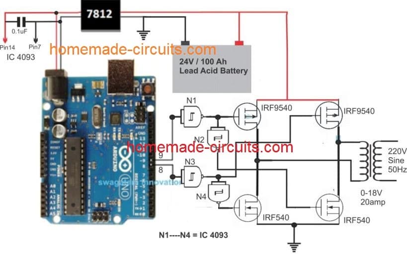
A simple yet useful Microprocessor based Arduino full-bridge inverter circuit can be built by programming an Arduino board with SPWM and by integrating a few mosfets with in H-bridge topology, I have explained the details below:
In one of our earlier articles I will comprehensively explained how to build a simple Arduino sine wave inverter, here we will see how the same Arduino project could be applied for building a simple full bridge or an H-bridge inverter circuit.
Using P-Channel and N-Channel Mosfets
To keep things simple we will use the P-channel mosfets for the high side mosfets and N-channel mosfets for the low side mosfets, this will allow us to avoid the complex bootstrap stage and enable direct integration of the Arduino signal with the mosfets.
Usually N-channel mosfets are employed while designing full bridge based inverters, which ensures the most ideal current switching across the mosfets and the load, and ensures a much safer working conditions for the mosfets.
However when a combination of and p and n channel mosfets are used, the risk of a shoot through and other similar factors across the mosfets becomes a serious issue.
Having said that, if the transition phases are appropriately safeguarded with a small dead time, the switching can be perhaps made as safe as possible and blowing of the mosfets could be avoided.
In this design I have specifically used Schmidt trigger NAND gates using IC 4093 which ensures that the switching across the two channels are crisp, and it's not affected by any kind of spurious transients or low signal disturbance.
Gates N1-N4 Logic Operation
When Pin 9 is logic 1, and pin 8 is logic 0
- N1 output is 0, Top Left p-MOSFET is ON, N2 output is 1, the Lower Right n-MOSFET is ON.
- N3 output is 1, Top Right p-MOSFET is OFF, N4 output 0, Lower Left n-MOSFET is OFF.
- The exactly same sequence happens for the other diagonally connected MOSFETs, when pin 9 is logic 0, and pin 8 is logic 1
How it Works
As shown in the above figure, the working of this Arduino based full bridge sinewave inverter can be understood with the help of the following points:
The Arduino is programmed to genearte appropriately formatted SPWM outputs from pin#8 and pin#9.
While one of the pins is generating the SPWMs, the complementary pin is held low.
The respective outputs from the above mentioned pinouts are processed through Schmidt trigger NAND gates (N1---N4) from the IC 4093. The gates are all arranged as inverters with a Schmidt response, and fed to the relevant mosfets of the full bridge driver network.
While pin#9 generates the SPWMs, N1 inverts the SPWMs and ensures the relevant high side mosfets responds and conducts to the high logics of the SPWM, and N2 ensures the low side N-channel mosfet does the same.
During this time pin#8 is held at logic zero (inactive), which is appropriately interpreted by N3 N4 to ensure that the other complementary mosfet pair of the H-bridge remains completely switched OFF.
The above criteria is identically repeated when the SPWM generation transits to the pin#8 from pin#9, and the set conditions are continuously repeated across the Arduino pinouts and the full bridge mosfet pairs.
Battery Specifications
The battery specification selected for the given Arduino full bridge sinewave inverter circuit is 24V/100Ah, however any other desired specification could be selected for the battery as per the user preference.
The transforer primary voltage specs should be slightly lower than the battery voltage to ensure that the SPWM RMS proportionately creates around 220V to 240V at the secondary of the transformer.
The Entire Program Code is Provided in the following article:
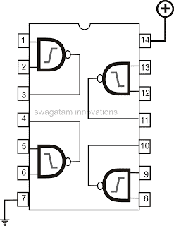
4093 IC pinouts
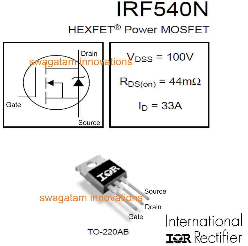
IRF540 pinout Detail (IRF9540 will also have the same pinout config)
An Easier Full-Bridge Alternative
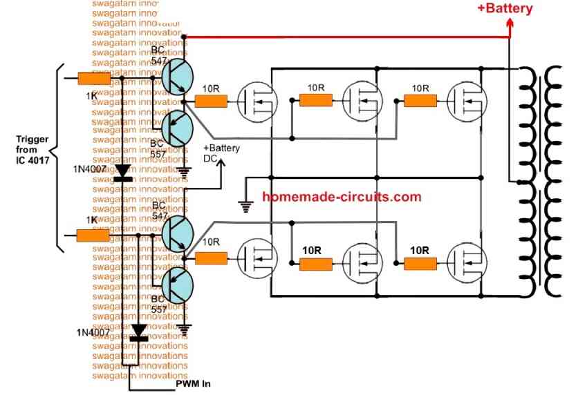
The figure below shows an alternate H-bridge design using P and N channel MOSFETs, which does not depend on ICs, instead uses ordinary BJTs as drivers for isolating the MOSFETs.
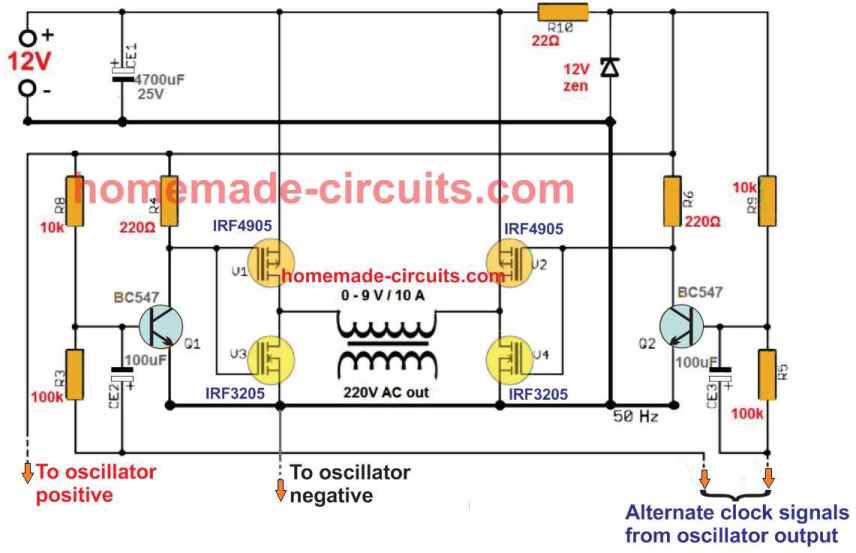
The alternate clock signals are supplied from the Arduino board, while the positive and negative outputs from the above circuit is supplied to the Arduino DC input.



Questions & Answers
thanks Swag for the update and correction in diagram i’v tried the simulation with TL494 an the input cd4093 and it works fine as a modified sine so am gonna build this and see sine i like h-bridge more than centered type.
pics attached
http://www.mediafire.com/?96fb9vdahpidh
Thank you very much Nito, I hope you succeed with your project, but remember TL494 is specified to work with minimum 1000 Hz so it might not work correctly below this frequency
Thanks once more for the info. Will SG3525 be okay if i use, from the data sheet it’s frequency is 100 Hz to 400 kHz and i already have one circuit built as well as the TL494.
am yet to get 4093 ic to test the whole project
yes SG3525 will be OK, alternatively IC 4047 can be even better
Hi Swag, do I have to bridge the paired inputs on the 4093, Ie Pin’s 1 & 2; 5 & 6 etc?
Regards D
Hi Dylan, yes the inputs of all the gates will need to be shorted.
Thank you Sir!
I built it this morning: https://imgur.com/a/xrMajrw
Will connect it up tonight after I get home from work
That’s great Dylan, I wish you all the best, just make sure the mosfets are correctly connected before you apply power….
Hi Swag, I built the system and it seems to be working. I used a 12V power supply boosted up to 24V in place of the batteries and I was able to get an AC reading on both sides of the transformer. The problem is I am only getting 4V there. Is this because of the power supply?
Thanks again for taking the time to help me out 🙂
Hi Dylan, yes it could be due to power supply, however the secondary should have shown higher voltage if both side mosfets are conducting correctly.
you can confirm the design with a 12V transformer and 12V power supply and check the response. Once confirmed you could then go ahead with 24V
Hi Swagatham , you blew my mind, I have a couple of none center tapped trafo`s from damaged driver inverters ranging from 24V, 36V , always love full bridge , I will try 24V , then 36V for 48V input output 240VAC
Thanks again
You are most welcome vhafuwi, keep up the good work.
Hello Swagatham , what is the alternative to IC4093
Hi vhafuwi, you can try IC4584B, and use 4 out of 6 available gates, and terminate the inputs of the unused 3 gate appropriately
Thanks for the prompt reply , Due to the simplicity of the circuit , I am constructing after testing I will design the PCB layout and order few boards ,
One question Though
For the SPWM output , what will be more efficient comparing Aduino Atmega328P / IC4047 /SG3525 , I have been considering IC4047 for its straight forward use ,
Any Idea how to get Puse Sine Wave out of IC4047 to feed in the above circuit.
Trying to get this circuit cheaper and efficient as possible
4047, 3525 cannot be used directly for creating SPWM, you may have to apply an external SPWM chopper to enable sine waveform from these ICs.
If Atmega is coded with SPWM just like the Arduino, then it might also work as effectively as the Arduino.
for 4047 yo can refer to the following post
https://www.homemade-circuits.com/pure-sine-wave-inverter-circuit-using/
Thanks Swag, I have a question, why you use or for what is use the IC 4047 in this circuit, I am a noob on electronics and I would like to know more about the IC 4047
Hi Ethan, IC 4047 is an oscillator IC, which has two outputs for generating a frequency with alternate ON/OFF switching, meaning when one of the two outputs is ON the other will be OFF and vice versa, the oscillation rate depends on the adjustment of an external resistor/capacitor values connected with another set of pinouts of the IC
Ok thanks, and I have a big question, what pin are conectted to which mosfet, can you explaine me, for example “pin 12 its conected to IRF9540”, like I said im a noob on this
The mosfet gates are connected to the NAND gates from the IC 4093, you can see the IC pinout diagram at the bottom section of the article, you can see which pins are internally connected with its internal NAND gates. Just compare the IC layout with the gates shown in between the Arduino board and the mosfets, you will get an idea how the IC 4093 needs to be configured
Sir is there any programming code require for this circuit
link for the code is given in the article, please check it.
Sir we realy appreciate with ur effort. please sir can u help me with pure sine wave inverter circuit using ATMEGA32 IC that include LCD DISPLAY
Hi Bashir, I do not have this design at the moment, if I happen to find it I’ll let you know…
thank u sir
Sir how r u? I have a duestion
we know sine wave inverter hard to design,
so what kind inverters are best for our normal house hold appliances? ( light, fan only)
Modified sine wave or PWM what is best?
Hi Mehedi, both will work, PWM inverter is also a kind of modified inverter but they are better than ordinary modified ones. If you apply proper filter stage at the transformer outputs both versions will work quite efficiently.
sir how are u? i have a question. In your 4093 ic logic, when pin 9 give pulse (=1). N1 = 0 and N2 = 0, so P channel (N1) = OFF and N channel (N2) = ON. Is it right? thanks
I am good Luna, thanks, When N1 input is high, its output is 0, this 0 is applied to the input of N2 causing its output to be “1” or high, this allows the opposite diagonally positioned fets to conduct simultaneously and keep the other diagonal fets switched OFF.
Oh thanks sir. GBU
You are welcome!
Thanks alot swag……can you mention? What ic and voltage regulator should i prefer when constructing same design for 45v dc supply…….
Hi Raghib, the easiest way is to use a transistor emitter follower regulator. Please see how the BC546 circuit is in the following article, for getting 9V
https://www.homemade-circuits.com/48-v-inverter-circuit/
Will it work i have input supply from 45v dc solar panel rating 300W to get a spwm unipolar based inverter (230v ac, 50Hz)where losses is minimum.How can i do please suggest me.Can i go for your full bridge inverter?How can i fixed ic and regulartor for 45dc input voltages.
Yes the mentioned emitter follower BC546 concept will work for 45V DC input. The base zener will fix the output voltage. The above Arduino is a bit complex so i wouldn’t recommend this to you since you are a newbie. Instead you can use your own unipolar design without issues.
Thanks swag……Will ic4093(maximum rating 18v) not burn?if we supply 24v dc.
It will definitely burn even at 20V, a 7812 IC can be used for preventing this issue.
Reply.
The mosfets were connected the wrong way and after fixing that we got the pwm pulses.
Thank you for your kind cooperation.
That’s great Vignesh, let me know if you have any further issues with the design
Please sir can u help me with cascaded H-Bridge 5 level inverter circuit using arduino
Hi Dhams,
I’ll investigate, and If it’s possible, I will surely try to update it.
Hello sir,
We tried to build the circuit as shown on the breadboard,but unable to get the output as spwm. Can you suggest what probable mistakes we might have made.
Hello Vignesh,
What kind of output are you getting? I have not yet tested this circuit practically but I believe if it’s built correctly it will surely work.
But on breadboard the mosfet may have a high possibility of blowing even with minor hidden issues
Hi Swag!
Did you test this circuit, with Arduino code, IC4093 and MOSFETS in bridge? is it necessary to use both, so P-channel and N-channel? If I understand right, P-channel and N-channel is here because of transition, when the first 10ms period ends and second 10ms period starts, so that transition between periods is not dangerous for MOSFETS? If I use delay and use relay on +12V line, then I could use just N-channels? Will be 9V/230V transformer ok for 12V battery, we calculated the rms value of 12V to 8,5V rms with Arduino signal, so it could be ok?
Thanks for answer, Serđ.
Hi Serd, As per the standard transistor biasing rules the source or the emitter must get the “ground” reference for operating through a normal base/gate switching.
That’s why p-channel is used on top and n-channel on bottom so that p gets the required positive “ground” reference and the n gets the negative “ground” reference.
If all 4 n-channel fets are used then the situation gets complex and requires bootstrapping a explained here:
https://www.homemade-circuits.com/h-bridge-bootstrapping/
The p channel n channel will also work but the p channel might show some significant heating due to incompatibility with n channel switching and higher R(ds) than n-channel.
The transition is perhaps handled correctly here, with the help of a “LOW” between the Arduino code sets, and also by the use of Schmidt trigger NAND gates IC 4093.
I have not yet tested this design practically!!
Thanks for your answer. So I don`t have to change Arduino code, because there is “LOW” command for signal, at the end of first and second period. Now I understand better, why to use P-channel at top and N-channel at bottom.
That’s right Serd, Glad it helped!
I will use 9V/230V – 200W or 300W transformer with 12V car battery. If I use 200W or 300W, I can expect the primary current of: 200W or 300W / 9V= 22A or 33A. Let`s say that I use 300W, that mean current consumption of max. 33A on battery side.
N channel IRF540 datasheet is (100V and 33A) and P-channel IRF9540 (100V and 19A). Are max. current limits of MOSFETS added together, so 33A+19A= 52A? Or is better to use N-channel IRF3205 (55V and 110A) and P-channel IRF9540 (55V and 74A) with that power of transformer?
The 33A will be the maximum current delivering capacity of the transformer, but actually 33A will be consumed only when the load is 33 amp, so it will depend on the load.
Current will not add across the mosfets, it will be 33A only, so both the mosfets can be rated at around 40A, higher values than this will also do.
Yes the last two mosfets look good and can be used.
So, if I understand right, the current in that schematic is limited to 19A, because the P-channel IRF 9540 MOSFET has 19A max. current limit, this means about 200W with 9V transformer? It doesn`t matter, if IRF540 has higher current limit, max. current of IRF 9540 is 19A, so 19A is max. current through. The current limits for both MOSFETS should be closely together. Let me know, if I`m right.
The mosfet with lower current rating will start heating up fast and might ultimately burn. So for a 19 A device the load current cannot be increased above 19 amp, in fact not above 15 amp to avoid too much stress on the mosfet. The mosfet current rating must be sufficiently higher than the maximum load current you intend to use at the output.
Hi Swag,
So I don`t need to use delay ON timer and relay on positive wire, which is going to mosfets, if I`m using H-bridge configuration, or is better to use it?
How can I use voltage regulator with opamp741 with IC4093? Use opamp741 output transistors in series with resistor connected to output pins 8 and 9 of Arduino and then connected to ground? – so when the voltage is to high, transistors will short the signal through resistor(10Kohm) to ground and there won`t be any signal on pins of 4093?
Thanks for your help.
Hi Serd, delay ON will be required for this project also, because during initial switch ON, the Arduino outputs could be in an undefined status causing the mosfets to conduct abnormally and blow.
You can connect the output of 7812 to the Arduino, 741 circuit and the 4093 circuit, all together commonly.
The output from the following circuit (BC547s) can be connected to the IRF540 gates. Just make sure to use a 220 ohm between the IRF540 gate and respective NAND outputs
Hi Swag,
I think, that is good idea to add delay ON to positive wire with relay too.
“The output from the following circuit (BC547s) can be connected to the IRF540 gates.”
So, if I understand right, I can connect opamp741 voltage limitor output directly to both bottom IRF540 and that will cause that the gate of IRF540 will be connected to ground when output voltage is too high and IRFs won`t conduct. I think, you meant that for previous design, with center tapped transformer, not this one with H-bridge. Correct me if I`m wrong. How to implement this with that design, so H-bridge?
In my opinion, better idea is to connect Arduino output pins, with BC547 outputs (opamp 741 voltage limitor circuit) to ground. That will cause logical “0” on Arduino pins and so on IC4093 input pins and all MOSFETS will be closed.
“Just make sure to use a 220 ohm between the IRF540 gate and respective NAND outputs.”
It is generally a good idea to include a gate resistor to avoid ringing (parasitic oscillation). A low ohm resistor will solve the ringing. I think the typical value of 10-100 ohms from IC4093 outputs to each MOSFET gates in bridge, could be just ok. Why did you choose 220 ohm? It`s good idea to add a high value resistor (about 10Kohm) from the each gate of P-channel MOSFETS to positive voltage (pull-up resistors) and each gate of N-channel MOSFETS with 10Kohm resistor to ground (pull-down resistors). Anyway, the good thing is that there is IC4093 Schmidt trigger and it provides full switching of MOSFETS (fully open or closed) and there is no “floating” voltage on gates, thanks to Schmidt triggers.
Thanks for helping me out. I will try to make this design practically when I get all components.
Hi Serd, Sorry I forgot add the opamp circuit diagram, here it is:
I was referring to the full bridge only not the center tap. The BC547 collectors can be connected with the low side n-channel mosfet with the gate connected to N2/N4 through a 220 ohm resistor. The 220 ohm would also work since the frequency is only 50 Hz, enough time to discharge the mosfet capacitance through the 220 ohm also.
If you are doubtful then you can add a BC547/BC557 buffer between N2/N4 and the mosfets, and then integrate this buffer with the volatge limiter as done here:
Shunting any circuit output is inappropriate, therefore Arduino output cannot be connected with the voltage limiter, this may lead to high dissipation and may be harmful to the Arduino.
….yes Schmidt triggers are good, but only the p-channel and n-channel combination is not so good 🙂
Ok. So I must add gate resistor (10-220ohm) from N2/N4, to gates of lower N-channel mosfets and connect outputs with BC547 (opamp741 circuit), between gate resistors and mosfet gates. What about upper P-channel mosfets? Don`t they require gate resistor from N1/N3 too?
Thanks.
If you use anything less than 100 ohm that will cause 4093 to heat up and dissipate, that’s why I recommend 220 ohm, alternatively you can use 220 ohm in series with 4093 Vcc (+) pin, and then use 10 ohms with N2/N4, this will do the trick.
the upper and the lower mosfets are in series, so any one of them can be used for feeding the pwm.
….yes you can use 10 ohm for upper mosfets also…
Hi Swag, appreciate your effort, I have a question related to that circuit. How can I control the output voltage of this full bridge inverter? Have you done any study about that ? As I have researched a comparison between output and a reference voltage (feedback) is needed but I am not sure how to make it. Thanks in advance
Thanks Blendi, You can control the output by upgrading the code such that one of the Arduino pins accepts an input from a feedback to adjust the PWMs fed to the NAND gates. I am not good with Arduino coding therefore for me it may be quite difficult to accomplish this.
Hi Sir, I have used this full-bridge circuit with 2 P-channel and 2 N-channel mosfets (this one in the top of the page) and I have supply the circuit with 6V DC so as a result I have received approximately 4V AC (peak to peak) in the output. Have I received the right result or not (why it is lower than our 6V DC)? In addition I wanted to know if using bootstrapping circuit with 4 N-channel mosfets full-bridge (The last one) is safer than this one with 2 P-channel and 2 N-channel mosfets or not ? Which one do you recommend and why ? Thanks in advance
Hi Blendi, 4V is correct because the output from Arduino is PWM in the form ON/OFF 6V supply…therefore due to the OFF periods the average will be lower than 6V.
The lower circuit has not been investigated thoroughly by me yet, but the first one looks fine in every respect, the only thing that needs to be considered is the selection of the p channel mosfet which must have an RDS(on) similar to the low side N mosfet. You can read more about it here
https://www.homemade-circuits.com/how-to-implement-p-channel-mosfet-in-h-bridge-applications/
…by the 4V is not peak to peak, it’s the average value, the peak will be 6V…also this is not AC, it is pwm DC
Do you have any e-mail address in order to send my result (The oscilloscope output) to you ? Because I couldn’t understand you last sentence.
Good morning, Swag.
I have a mini system transformer I would like to use as an inverter of 12v x 110v x 100w, but I only know that there are 2 wires in the secondary and 5 in the primary. I do not know which wires connect to make the 110v, its voltage or amperage.
Could you help me identify the wires and fit the inverter design with only two wires in the primary of this inverter?
I have in primary between pins 1 and 2: 39.4 ohms.
Between pins 3 and 4: 26.3 ohms
Between 3 and 5: 40.8 ohms
Between 4 and 5: 37.3 ohms.
On the secondary: 28 ohms.
* approximate measures.
Tanks
Hi Marcelo, You will need grid supply 110V to test the transformer. Plug in two wires into mains 110V socket, one wire having a 60 watt or 40 watt bulb in series. Now cautiously touch the wire ends randomly across the transformer pins. The pair of pins that allows minimum glow or zero glow on the bub will be your 110V winding of the transformer.
Once confirmed connect the mains wires along with the bulb across those pins, and with a AC voltmeter start checking the outputs across the other pins of the transformer, and note down the corresponding data.
I did as you said, using a 40w bulb.
1 and 2: very weak
3 and 5: very weak
4 and 5: weak
3 and 4: strong.
The other combinations did not signal the filament of the lamp. I’m sorry, but I still do not know which wire to connect.
Thats transformer have 110v, 127v, 220v e 240v.
From the winding which did not give any glow check there resistances, the one with lowest resistance will be 110V…connect the 110V AC with series bulb across this winding and measure the voltages from the other wires to know their details.
Please sir I have some challenges in this high bridge inverter.
you can specify them, will try to solve it!
Hi swag,
How can i convert 280 volts DC from set of solar pannels to 230 volts AC 50hz
sine wave without using regulator and battery
Thank you.
Hi Lahana,
you can try one of the designs from the following article:
https://www.homemade-circuits.com/5kva-transformerless-inverter-circuit/
thank you so much for your help, what if i use your design with
4 n-chanel mosfets and arduino ?can i get 230 volt AC from 280 volt dc
Yes that’s possible, but you will need a full bridge IC for that and switch it’s low side MOSFET with Arduino PWM. This might look like an overkill, because SPWM can be implemented in full bridge through synchronized op amp circuit also.
Hi sir,
I can’t find CD4093 ic in local market. Can i use any NAND gate replacement of this?
Or is there any suitable replacement of CD4093 ?
Please reply asap.
Thank you.
Hi Sourav, 4093 is very popular, and should be available everywhere. Thee’s no other easy alternative for this, because others are 5V rated which will not work for MOSFeTs.
The prefix CD is not important you can use any 4093 version.
Finally if you don’t get 4093, you can go for any standar 12V NAND gate IC
Did anyone made this circuit as drawn in schematic and made it actually work properly? If yes, the circuit goes beyond my knowledge in electronics (MOSFET operation principle in particular). If not, than I’d ask Mr. Swag to build the circuit, test it and if it doesn’t work for him either to fix the schematic or remove it from the Internet.
Better explain your point instead of giving opinions.
I am creating the same scheme. Im using 6V DC input.How much AC can I take.
How can I calculate the output
hi
If i`ll add pullup/pulldown resistors (G to S) would be any better ?
I`m wondering if there will
Thank you
yes you may try that for added safety to the MOSFETs
considering that there is 12V on the mosfet gate and the mosfet is rated 10V or -10V would be any good idea to add 1k resistor from N to G?
Thank you
Marius
you can connect a 1K from gate to source under all situations.
ok so i build one
the P-channel mosfets are overheating …
i`m trying to invert 24VDC to VAC for a project, seems that i have to chose a different way
thank you
Marius
The major drawback of using P channel is its heating up issue….we have to make sure that the RDSon of the pchannel is equal to the RDSon of the N channel…this can be done by adding more number of P channels in parallel.
So you can try using a couple of more p channel MOSFETs in parallel, that should solve the problem in my opinion.
another thing what i`m thinking about is that because that H bridge is paired as X
i mean mosfet 1 is paired across X with mosfet 4 and not with mosfet 3
I`ll try to pair the mosfet 1 with 2 and 3 with 4 to see the results
thank you
If you pair MOSFET 1 with 2, then how will the load operate? It has to be in diagonal form, otherwise the load cannot switch
The alternate clock input terminals must be integrated with the NAND gate outputs which will act like level shifters here.
hallo , can you explain to me about this word in above,
how to integrated NAND gate output with alternate clock
how to set transformer value in proteus? secondary and primary
Hi,
I am just trying to understand how the above circuit works and I have implemented it but it does not work correctly for me and I will need too to modify it later on. I don’t understand some details:
1) The 4093 is fed with the battery voltage 12V. Will it output as logic true: 12V or 5V ? Can I change the battery voltage to 24V or 48V ?
2) In one case used 5V DC for driving the whole instead of 12V and after I took off the Vcc from the 4093 but it continues to drive normally the whole circuit probably using power from the arduino input. Should it be like that ? Isn’t a little bit strange ?
3) I used as a shortcut to drive the mosfets from 2 outuput gates only instead of 4. The system works but probably get’s hot because there is no delay between switching on and switching off … is it like that ?
4) I need a modified circuit that will work from direct current 110V without a transformer. How should I change the components ?
Hi, the circuit has to work since the NAND gate implementation looks logically perfect. The output from the NANDs will be 12 V if the IC is operated with 12 V…if it is operated with 5 V the MOSFETs will misbehave and not work correctly.
If you remove the 12 V supply from the NAND gate IC, again the system may behave weirdly and malfunction.
Using two NAND gates is absolutely incorrect and may easily burn the MOSFETs.
You must first try to implement the 12V design correctly, after that you can try the 110 V upgradation.
As per the characteristics of the CD4093B found here https://www.ti.com/lit/ds/symlink/cd4093b.pdf it seems that the CD4093B if fed with 10V (instead of 12) needs typically (at ambient temperature ) 5.9V in order to accept it as a logical 1.
I deduced it from page 2 “positive trigger threshold voltage” at 25C “typical”.
How is it possible then that the arduino fed at 5V is able to trigger the logical 1 condition ?
Anything above 4 V is accepted as logic HIGH for any logic IC at 12 V. 5 V is logic 1 without any doubt. 4093 is a Schmitt trigger IC so rules could be different….Better check it practically by connecting the input directly to 5 V and checking the output. Alternatively you can try replacing the gates with 4049 NOT gates.
Please sir, check this circuit if i made it correct and i got from this site and i made little modification https://drive.google.com/drive/mobile/folders/1Ld6NO3ZIq7EDEkf4RT2GUkVT6ELhN2ST?sort=13&direction=a
Bashir, It is not opening in my computer
I have paste the schematic to your facbook timeline you can check it please
The full bridge design is correct
Thank you sir