In this post we are going to take a look at the popular LM 324 IC. We will be looking at the pin configuration, its important features and its technical specifications and finally we will be looking at some of the fundamental application circuits using LM 324.
If you are looking for a low voltage operational amplifier (3V and above) IC which can work on single and dual power supplies with wide range of frequencies and with minimal power consumption, then LM324 can be the best suited for your design. It is available as THT or through hole technology and SMD or surface mound device packages.
Now let’s look at the key features:
Main Features
• It can operate from 3 V to 30 V single power supply.
• It can operate from +/- 1.5 V to +/- 15 V for dual supply.
• It has bandwidth up to 1.3 MHz
• Large voltage gain of 100 dB
• 4 independent amplifiers.
• Some of the variants are short circuit protected at the output.
• True differential input stages.
• Very low current consumption: 375 uA.
• Low input bias current: 20 nA.
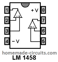
Next we'll take a look at the pin diagram of LM 324:
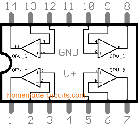
Pin Description:
There are 4 individual amplifiers / op-amps.
• Pin #1 is the output for first amplifier (left bottom)
• Pin #2 and #3 are the input for the first amplifier.
• Pin #4 is Vcc who’s maximum input voltage is 30V / +/-15V.
• Pin #5 and #6 are the input for second amplifier (right bottom)
• Pin #7 is the output for second amplifier.
• Pin #8 is output for third amplifier (right top)
• Pin #9 and #10 are two inputs for third amplifier.
• Pin #11 is ground.
• Pin #13 and #12 are inputs for fourth amplifier (top left)
• Pin #14 is the output for fourth amplifier.
• (+) represents non inverting input.
• (-) represents inverting input.
Absolute Maximum ratings and operating conditions:
Absolute maximum ratings are at-most limit of the component beyond which the component will not work as described / get damaged permanently.
Supply voltage: If your supply is dual supply (absolute) maximum is +/- 16V. If your power supply is single supply 32VDC.
Input differential voltage range: +/- 32 VDC: This range refers to the voltage difference that could be applied across the input pinouts of each of the opamps.
Input common mode voltage range: -0.3 to 32 VDC: These are the maximum and the minimum common mode input signal levels that may appear across the inputs of the opamp.
Junction temperature: 150 degree Celsius: It is the temperature that should not be exceeded at any cost on the IC, otherwise that mat cause a permanent damage to the IC
Power dissipation: 400 milliwatt: It is the amount of heat dissipation that the IC can withstand, and the limit at which its junction temperature could rise to 150 degree Celsius. Although this may be corrected with a heatsink, ICs should never be subjected to direct high power loads without appropriate buffer stages.
Storage temperature: -65 to +150 degree Celsius: Nothing critical here, as the range is well within any country's climatic conditions.
Operating ambient temperature: 0 to +70 degree Celsius: While operating the IC, the ambient or the surrounding temperature must be ideally below 70 degrees Celsius otherwise unpredictable things can occur with the IC performance.
Electrical characteristics (VCC+ = 5 V, VCC- = Ground, Vo = 1.4 V, Temp = 25 °C)
• Input offset voltage: typical: 2 mV, maximum: 7 mV.
• Input offset current typical: 2 nA, maximum: 20 nA.
• Input bias current typical: 20 nA, maximum: 100 nA.
• Large signal voltage gain ( Vcc = 15 v, RL, = 2 kohm, Vo = 1.4 V to 11.4 V): min: 50 V/mV, max: 100 V/mV.
• Slew rate (Vcc = 15 V, Vi = 0.5 V to 3 V, RL = 2 Kohm, CL = 100pF, unity gain) typical: 0.4 V/uS
• Output current source [Vid = 1 V] (Vcc = 15 V, Vo = 2V): minimum: 20 mA, Typical: 40 mA, Maximum: 70 mA.
• Output sink current [Vid = -1 V] (Vcc = 15 V, Vo = 2V) Minimum: 10mA, Typical: 20 mA.
• High Level Output Voltage (Vcc = 30 V, RL = 2 K ohm) Minimum: 26 V, Typical: 27 V.
• High Level Output Voltage (Vcc = 5 V, RL = 2 K ohm) Minimum: 3 V.
• Low Level Output Voltage (RL = 10 k Ohm) Typical: 5 mV, Maximum: 20mV.
• Total harmonic distortion (f = 1kHz, Av = 20 dB, RL = 2 kΩ, Vo = 2 Vpp, CL = 100 pF, VCC = 30 V) Typical: 0.015 %.
• Gain Bandwidth Product (VCC = 30 V, f = 100 kHz, Vin = 10 mV, RL = 2 kΩ, CL = 100 pF ) Typical : 1.3 MHz.
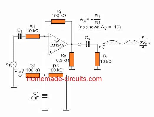
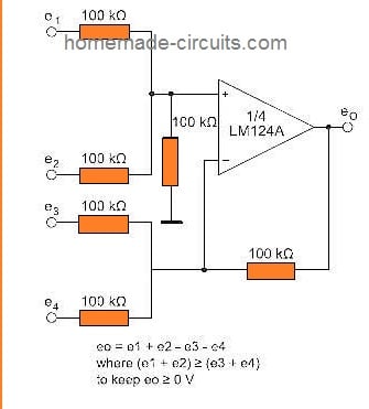
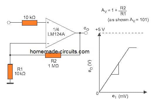
Application circuits:
AC coupling Inverting Amplifier:
DC summing Amplifier:
Non Inverting DC Gain:
Feel free to report any errors or questions via comment section you may get a quick reply.
Comments (28)
I am currently using a MC34071P op amp which is discontinued , is there an op amp out there that will replace the MC 34071P.
I think you can use LM358, but this op amp can handle only upto 32 V whereas MC3401 can work with upto 44V.
Thanks for the info , I will look into it
Lorne
What about equivalent circuits using a dual power supply.
thank you very much. it is very helpful.
You are most welcome!
Sir,
8pin ic is burned..how to find the ic part number …
1&8 pin is +VCC 5v supply.
2pin is connect on varaible resistors.
3pin is not connected.
4pin is gnd.
5pin is output.
6pin is input
7pin is led output.
But once sense the sensor input the 7pin output led is continuously on & 5pin relay only once on..again sensing twice time of the sensor input the led is off…routine the operation..
Manivannan, sorry, cant figure it out, it is very difficult to judge just by its pin number assignments.
Me interesa mucho compartir con usted. Soy técnico de electrónica, vivo en Cuba pero no se inglés.
Soy Polaco y hablo español un poco. Puedo ayudarte, soy técnico de electrónica también y conozco inglés. Si tienes los preguntas, no es problema para mí. Mi correo es krzysiekdete@interia.pl. Saludo!
No problem, you can ask your questions through Google translate….
Hi sag how do i make a flasher with LM324N ic
Hello, you need to make an oscillator with an op amp. Search op amp datasheet on Google. Also google “oscillator circuit with op amp”. Positive feedback is the basis of making an oscillator with op amp
what kind of flasher, LED flasher or lamp flasher?
Is there any circuit of Automatic plant Irrigation systems using LM324&IC555.
Please reply…
There’s one circuit using IC 741 as given below, you can create 4 of these using a single iC LM324
https://www.homemade-circuits.com/soil-moisture-tester-circuit/
Thanks
Can you please direct me on how to use this same ic to build stabilizer circuit?
It is explained under this post:
https://www.homemade-circuits.com/5-kva-to-10-kva-automatic-voltage-stabilizer-circuit-220-volts-120-volts/
Hi Swag,
I am new to electronics and am in the process of trying to work out the circuit for a solar tracker which uses an H bridge in conjunction with an LM1458 I.C.. I found it on this website. I was considering purchasing it from him, but his webpage is primitive and lacks an order/pay page, so I decided to make it myself.
It seemed as though it would be easy to build but I am confused about 2 things so far. One is that the circuit he used shows the positive on one amp in the I.C. connected to the negative of the other amp. Would that be correct? Also, I am confused with the data sheet for the LM1458 as it shows no output on the top of amp “A”, yet pin 1 is labelled as the output for A. Do you know why they don’t show a connection between them?
I appreciate your time in reading and answering my questions Swag.
Regards,
Jim
Hi Jim,
You can organize the pins exactly as per the datasheet layout.
Here’s the image you can follow:
You can also use LM324 as given here:
https://www.homemade-circuits.com/how-to-build-dual-solar-tracker-system/
Thank you once again for your personal advice Swagatam. The circuit you suggested looks very easy and contains all necessary information unlike many on the net which often leave out vital information. Cheers!
Thank you Jim, Glad you found the data helpful!
Pls, I can’t find the best way to use lm324 as a comparator.
PLease read this:
https://www.homemade-circuits.com/how-to-use-ic-741-as-comparator/
all opamps work in similar way.
I Think you R doing a great job I love to look at all the circuits that you all post . Keep it up thanks
It’s my pleasure Roger, please do keep visiting and sharing…
I surely will I love all your circuits and the way they are displayed so thanks again and please keep up the good work.
I appreciate it 🙂