A simple yet useful Microprocessor based Arduino full-bridge inverter circuit can be built by programming an Arduino board with SPWM and by integrating a few mosfets with in H-bridge topology, I have explained the details below:
In one of our earlier articles I will comprehensively explained how to build a simple Arduino sine wave inverter, here we will see how the same Arduino project could be applied for building a simple full bridge or an H-bridge inverter circuit.
Using P-Channel and N-Channel Mosfets
To keep things simple we will use the P-channel mosfets for the high side mosfets and N-channel mosfets for the low side mosfets, this will allow us to avoid the complex bootstrap stage and enable direct integration of the Arduino signal with the mosfets.
Usually N-channel mosfets are employed while designing full bridge based inverters, which ensures the most ideal current switching across the mosfets and the load, and ensures a much safer working conditions for the mosfets.
However when a combination of and p and n channel mosfets are used, the risk of a shoot through and other similar factors across the mosfets becomes a serious issue.
Having said that, if the transition phases are appropriately safeguarded with a small dead time, the switching can be perhaps made as safe as possible and blowing of the mosfets could be avoided.
In this design I have specifically used Schmidt trigger NAND gates using IC 4093 which ensures that the switching across the two channels are crisp, and it's not affected by any kind of spurious transients or low signal disturbance.
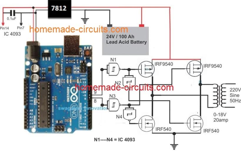
Gates N1-N4 Logic Operation
When Pin 9 is logic 1, and pin 8 is logic 0
- N1 output is 0, Top Left p-MOSFET is ON, N2 output is 1, the Lower Right n-MOSFET is ON.
- N3 output is 1, Top Right p-MOSFET is OFF, N4 output 0, Lower Left n-MOSFET is OFF.
- The exactly same sequence happens for the other diagonally connected MOSFETs, when pin 9 is logic 0, and pin 8 is logic 1
How it Works
As shown in the above figure, the working of this Arduino based full bridge sinewave inverter can be understood with the help of the following points:
The Arduino is programmed to genearte appropriately formatted SPWM outputs from pin#8 and pin#9.
While one of the pins is generating the SPWMs, the complementary pin is held low.
The respective outputs from the above mentioned pinouts are processed through Schmidt trigger NAND gates (N1---N4) from the IC 4093. The gates are all arranged as inverters with a Schmidt response, and fed to the relevant mosfets of the full bridge driver network.
While pin#9 generates the SPWMs, N1 inverts the SPWMs and ensures the relevant high side mosfets responds and conducts to the high logics of the SPWM, and N2 ensures the low side N-channel mosfet does the same.
During this time pin#8 is held at logic zero (inactive), which is appropriately interpreted by N3 N4 to ensure that the other complementary mosfet pair of the H-bridge remains completely switched OFF.
The above criteria is identically repeated when the SPWM generation transits to the pin#8 from pin#9, and the set conditions are continuously repeated across the Arduino pinouts and the full bridge mosfet pairs.
Battery Specifications
The battery specification selected for the given Arduino full bridge sinewave inverter circuit is 24V/100Ah, however any other desired specification could be selected for the battery as per the user preference.
The transforer primary voltage specs should be slightly lower than the battery voltage to ensure that the SPWM RMS proportionately creates around 220V to 240V at the secondary of the transformer.
The Entire Program Code is Provided in the following article:
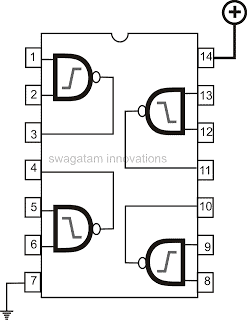
4093 IC pinouts
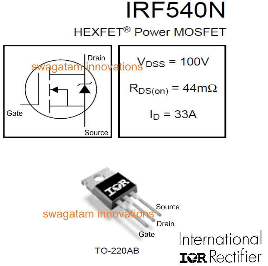
IRF540 pinout Detail (IRF9540 will also have the same pinout config)
An Easier Full-Bridge Alternative
The figure below shows an alternate H-bridge design using P and N channel MOSFETs, which does not depend on ICs, instead uses ordinary BJTs as drivers for isolating the MOSFETs.
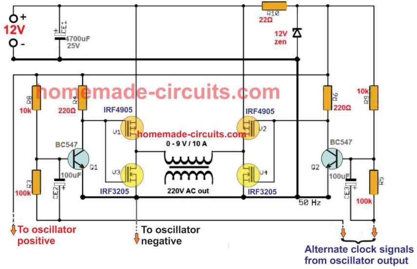
The alternate clock signals are supplied from the Arduino board, while the positive and negative outputs from the above circuit is supplied to the Arduino DC input.



Questions & Answers
Hi — thank you for responding so quickly — and thank you for identifying the Arduino unit:
but your answer concerning using two P-types in parallel – was not my question.
Not being familiar with the P-type MOSFET – my question was — can I use a 4420 driver to power a P-type MOSFET – or do I have to use the 4429?
Thanks in advance.
I checked the datasheet of 4420 and 4429, they look exactly similar to me, so any of these can be used for driving the MOSFETs.
Also, these drivers can be used with P-Channel MOSFETs and N-Channel MOSFETs, both.
Please correct me if I am wrong.
Hi — I’ve got a question concerning the IRF9540 Mosfets.
I’ve been using IRF 741 MOSFETs / TO 220 Case driven by 4420 / 6 A Drivers with great success.
Pertaining to the IRF 9540 MOSFETs your calling for — is there a similar P-Type match that you would recommend to match the IRF741?
Also- do you know if I should use the 4429 / 6 A driver for the P type – or will the 4420 driver work for both.
To be honest – I have never worked with P-type MOSFETs before – and am aware that they are a little slower than the N type MOSFET.
Finally – is there a particular Arduino that you use for the full-wave H-Bridge inverter?
Thanks in advance for any info you can send me
…You can use two of these MOSFETs in parallel for the P channel MOSFETs.
https://www.mouser.com/datasheet/2/308/FQB4P40-1192331.pdf
Hi, thanks for your interesting question.
You can use either the 4420 driver or the 4429 with the Arduino output for getting the intended full bridge output results.
https://ww1.microchip.com/downloads/aemDocuments/documents/APID/ProductDocuments/DataSheets/21419D.pdf
The Arduino is the standard UNO board.
Could you just use a stepper motor driver card and get square wave or sine by selecting microsteps?
Sorry, I am not sure if that’s possible or not.
Amazing article sir ! And how much the wattage of your design sir ? Thank you very much
Thank you Tom, The power of the inverter will depend on the transformer, battery and the MOSFET specifications, which can be upgraded to any desired levels.
The frequency is s 50Hz I’m using iron core for the transformer.
I want to design a 6000W pure sine wave inverter using 48v battery. My challenge is how to calculate the wire size for both primary and secondary kindly help to explain how I can calculate the wire size for both primary and secondary.
Thanks
Sorry, calculating a 6000 watt transformer can be difficult, I do not have the formulas for calculating such a huge transformer.
I wanted to know if the transformer is a 50/60 Hz current transformer made of silicon steel sheets. I have my doubts because, since it is SPWM, the frequency is much higher than those 50/60 Hz of a normal transformer.
In this case, would it not be necessary to have an LC filter at the output of the transformer?
Yes the transformer is an ordinary iron core step down transformer connected the other way round. Only capacitive filter becomes sufficient since the transformer secondary winding itself works like an effective inductor. I have added a 3uF/400V capacitor which converts the SPWM into pure sine wave.
Sorry for the continues questions, can supply be given from the DC power supply at the lab or should lead acid battery be used?
Thanks again, Mr.Swagatam
You can use any 12 V DC supply for testing, it can be from a 12 V battery or from a 12 V SMPS, just make sure it has adequate current supply for the transformer and the load.
Thank you sir
You are welcome Anooshka
And can I connect IC4093 Vdd to 12V directly?
Thank you in advance for your prompt reply
Yes 4093 can be connected to 12 V DC directly, however I would recommend using a 100 ohm 1/4 watt resistor in series with the positive supply of the IC, and also connect a 12 V zener, and a 1N4148 diode right across the supply terminals of the 4093 IC along with parallel connected 100uF/25V and 0.1uF capacitors, all these will ensure that the IC is not affected by the voltage spikes from the transformer
Also sir I wanted to know, while using 7812, it has 3 pins, input (12V/24V), ground and output. I had the following doubts.
How is 7812 output pin connected to the Arduino?
How is the 0.1uF connected?
It would be really helpful if you could explain the 7812 connection diagram.
Sorry for disturbing and thank you for your cooperation.
It is important to note that the battery for this project must be strictly a 12V battery, a 24V battery will not work and might burn the MOSFETs.
For the 7812 connection, the battery (+) will connect with the input of 7812, the battery (-) will connect with the ground of the 7812, the output (+) and the ground of the 7812 will go to the (+) and (-) of the Arduino socket respectively.
Thank you for your prompt response, lastly how is the 0.1uF capacitor across 7812?
The 0.1uF is shown for the 4093 IC which must be also supplied from the 7812 IC.
Across the input and output right sir? Because the middle pin will be grounded of 7812.
You have been a lifesaver, thanks a lot for your replies.
Anooshka,
The capacitor should be connected across the output and the ground of the 7812, one pin of the capacitor must always connect with the ground of the circuit or the device.
I am glad to help you!
So these protection elements will all come in series with Vdd of IC 4093 or is it connected between Vdd and ground?
No, only the 100 ohm resistor will come in series with the (+) supply line of the 4093.
The zener diode, 1N4148 diode, 100uF, 0.1uF all these will need to be connected across the (+)(-) terminals of the 4093
Thank you sir
You are welcome!!
Hi, I am doing the above project but I am using a 12-0-12 (500MA) transformer instead. I inferred that changing to 12V supply would be enough. I have few more doubts
1) Would there be any change to circuit, am I to provide a delay, in that case how could I do so?
2) Would there be any change to the code?
3) Is there any way to replace transformer just by using RL load?
Hi, If you use a 12-0-12V transformer and a 12 V battery, then with an SPWM Arduino code the output voltage from the transformer would be around 180 V only. You should use a 6-0-6V transformer instead.
Delay may not be required since 4093 IC has a schmitt trigger inside which will cause a slight delay in the operation of the two sides.
If you do not use a transformer then 220 V output may not be possible to achieve.
Thank you for your response
How do I get good Inverter board and software
You can get it from online stores like amazon.
Good morning, thank you for your article.
I would like to increase the power by putting 4x mosfets in parallel in the H-bridge (IRF9540+IRF540).
Is that possible ?
Do you have a low battery cutout planned for your UPS?
Thanks
Michael
Hello, you can try with single mosfets first and confirm the working of the circuit. Once confirmed then you can try adding more mosfets in parallel to increase the power output.
For a low battery integration you can try integrating the following concepts:
IC 741 Low Battery Indicator Circuit
Low Battery Indicator Circuit Using Two Transistors Only
Best Swagatam
If looked at the circuit and would like to know where the 4093 IC draws its power from? It is rated at 15V max input and the design has a 24V battery.
The p-channel mosfets would have to get 24V to switch off and then assuming the 4093 IC uses a 24V supply (which it can’t) the Vgs of the mosfets would be 0 or 24V with 24V being above the maximum Vgs of the mosfets.
Regards Tiaan
You are right Tiaan, the battery must be a 12V battery in that case! Thanks for pointing out the mistake.
The 4093 can draw the supply voltage from the 12V battery
hello dear sir project is isolated bidirectional dc dc converter kindly share circuite diagram
I don’t have it at this moment, if I find it will surely share it with you.
How to get Arduino code??
Code is already given in the above article.
Best Swagatam
Your projects are very helpful, I just want to know.
What should change in this circuit if I want to use a 12V/230V transformer and 12V battery?
Also should this circuit get a delay circuit and voltage regulation circuit like the 12V arduino inverter project you made?
Kindest regards
Tiaan
Thanks Tiaan,
you don’t need to change anything except the battery. Yes, there should be a delay around 10 seconds before the Arduino output can be connected with the 4093 inputs otherwise the mosfets can burn.
Best Swagatam
Your projects are very helpful, I just want to know.
What should be changed in the circuit if I want to use a 12V battery and 12V/230V transformer?
Kindest regards
Thank you Tiaan,
You only have to change the battery to 12V, that’s all, nothing else needs to be changed.
I want to follow your designs
Thank you, sure you can!
Hello, not sure if I am missing it here in the comments or not, but I am wondering if this is a push pull circuit, that if you use a neutral line you would say get two 110v lines, that combining them gives the 220v? (ie is this what is called split phase in the US.)
I am working on a solar inverter design using cobbled bits of info and have some experience with arduino so was hoping it could be a good method of supplying the logical control of the DC side to generate a much better than modified sine wave output of common inverters available off market. 🙂
Thank you for sharing your concern, yes the output of the inverter will be a push pull type and not split phase.
Please sir i need overload cut off diagram for inverter
You can try the opamp circuit from the following article:
https://www.homemade-circuits.com/low-battery-cut-off-and-overload/
I am building a 5level multilevel inverter as my project in school. I am using the h-bridge cascaded topology. I also want to use arduino to generate the signal for the gates of the mosfet. If I use the same switches say irfp460 for all the switches will it work fine? Thanks in anticipation of your reply
Good day, please can the same MOSFET be used for the high side and low side if the h-bridge?
If you are using a bootstrapped type H-bridge then all the MOSFETs can eb n channel and same, but for any ordinary h bridge the high side and low mosfets will be different.
Does this also apply to 5 level cascaded multilevel inverters?
what type of H bridge did you in your inverter?
Its a 5 level multilevel inverter that joins two Normal H bridge in series to get the desired 5 level. I want to know if I use the same switch for the eight switches, if it will work just fine
Okay, thank you
So please what do you suggest I do for the multilevel inverter
You can find some information in the following article:
https://www.homemade-circuits.com/wp-content/uploads/2021/04/multilevel-3-phase-inverter.pdf
Just the arduino for generating the switching signals
then it may not be possible use all the 4 mosfets with the same polarity
which IC is used for driving the H bridge?
Using Proteus to simulate h bridge inverter using arduino.should I use anything else e.g driver transistors bc547 or just 4093 OK.kindly how to upload simulation pics.kind regards john
Sorry I don’t use proteus, so can’t help with it!
good day ,
I will like to know what kind of transformer I should use to get 230 Vac using a 12 Vdc car battery.
Do I need 12V to 230V or 6V to 230 V transformer please ?
Thanks
Ambr
You can use 0-9V/220V for 12V battery
Sorry,
My Second statement would not work either.
I meant to say,
was to use P9 output to override N3 output via 1K resistor to N3 output modified with a 10K resistor.
p9-=+–|N1–>
| 1K
+——/\/\——-+
|
p8 >—–|N3>–/\/\–+–>
10K
This would Disable p8 if p9 is already High.
You design is interesting, but basic.
First, you have a Typo:
N1 output is 0, Top left p-MOSFET is ON, N2 output is 1, the lower right n-MOSFET is ON.
N3 output is 1, top left p-MOSFET is OFF, N4 output 0, lower left n-MOSFET is OFF.
Should be :
N1 output is 0, Top left p-MOSFET is ON, N2 output is 1, the lower right n-MOSFET is ON.
N3 output is 1, top RIGHT p-MOSFET is OFF, N4 output 0, lower left n-MOSFET is OFF.
Second, I would suggest that the N1 & N2 NAND and the N3 and N4 gates – drive the Upper Left & Right PFETs and the Lower Right & Left NFETs respectably. (Notice the Left / Right + Right / Left switch there) Else, you risk burning out your FETs if both p8 & p9 are High.
Third, I would suggest placing Pull-Down Resistors on p8 & p9 – to avoid spikes to your FETs at Arduino Bootup or if the P8 P9 Pins are in Zero-State.
Thank you for liking my basic design!
I have corrected the typo as pointed out by you.
With an Arduino it is highly unlikely for both the outputs getting high at the same time, still it may be important to have some kind of foolproof arrangement to counter the issue, I’ll surely think about it.
hello mr swag i have been trying your innovative circuit post and they have worked greatly but I wish to know if you have any h bridge inverters that is sine wave but not Arduino thanks a lot
Thank you Ifeanyichukwu,
You can convert an H bridge into sine by feeding a SPWM to its low side MOSFeT
https://www.homemade-circuits.com/diesel-generator-rpm-controller-circuit/
In this example it is only an ordinary PWM and not SPWM
Ok thanks a lot sir
Hi Swagatam,
Please assist me with the following.
Ref. Home Inverter Circuits Arduino Full-Bridge (H-Bridge) Inverter Circuit
I want to use a 250VA 220/32V transformer as the final output in my inverter. My total load is 160W. I therefore need to modify the secondary by removing some windings until I get 9V output. The question is will the transformer then be able to cope with a 160W load. I would hate to ruin a good transformer if it is not going to work.
Regards
Jan
Hi Jan, the wattage of the transformer is calculated by multiplying the V x I values of the winding. So if the V and I of the transformer winding is sufficiently rated to handle around 200 watts then the output will be capable of handling 160 watt easily.
Hi,
I have following questions,
1. How much wattage we can achieve with this inverter?
2. For higher wattage, do we need to design heat sink ?
3. is the output of transformer 220V, 50Hz, sinusoidal?
Thanks !
Wattage will depend on the MOSFET, transformer and battery rating, which can upgraded to any desired magnitudes.
Heatsink will e required for the MOSFETs can be tested through practical experimentation.
Output is sine wave. Frequency is 50 Hz
Hi Swag why the voltage output from the mosfet became drop into 1.3V. im using 12V as the input voltage
https://imgur.com/Fj4Y8eN
Hi Jack, Please try to figure it out yourself, because only diagonally mOSFeTs can be ON at any instant, all the MOSFETs can be never be ON.
Please check the logic sequence just under the diagram to understand how the N1–N4 gates are supposed to work, and how all the MOSFeTs can never turn ON together.
How many watts can take by this inverter? I have a transformer which removed from a 24v 1000va ups and hope to use that for this inverter.
for 24-0-24V transformer you will need a 36 V battery, and current of 45 amps
Thank you sir
I have paste the schematic to your facbook timeline you can check it please
The full bridge design is correct
Please sir, check this circuit if i made it correct and i got from this site and i made little modification https://drive.google.com/drive/mobile/folders/1Ld6NO3ZIq7EDEkf4RT2GUkVT6ELhN2ST?sort=13&direction=a
Bashir, It is not opening in my computer
As per the characteristics of the CD4093B found here https://www.ti.com/lit/ds/symlink/cd4093b.pdf it seems that the CD4093B if fed with 10V (instead of 12) needs typically (at ambient temperature ) 5.9V in order to accept it as a logical 1.
I deduced it from page 2 “positive trigger threshold voltage” at 25C “typical”.
How is it possible then that the arduino fed at 5V is able to trigger the logical 1 condition ?
Anything above 4 V is accepted as logic HIGH for any logic IC at 12 V. 5 V is logic 1 without any doubt. 4093 is a Schmitt trigger IC so rules could be different….Better check it practically by connecting the input directly to 5 V and checking the output. Alternatively you can try replacing the gates with 4049 NOT gates.
Hi,
I am just trying to understand how the above circuit works and I have implemented it but it does not work correctly for me and I will need too to modify it later on. I don’t understand some details:
1) The 4093 is fed with the battery voltage 12V. Will it output as logic true: 12V or 5V ? Can I change the battery voltage to 24V or 48V ?
2) In one case used 5V DC for driving the whole instead of 12V and after I took off the Vcc from the 4093 but it continues to drive normally the whole circuit probably using power from the arduino input. Should it be like that ? Isn’t a little bit strange ?
3) I used as a shortcut to drive the mosfets from 2 outuput gates only instead of 4. The system works but probably get’s hot because there is no delay between switching on and switching off … is it like that ?
4) I need a modified circuit that will work from direct current 110V without a transformer. How should I change the components ?
Hi, the circuit has to work since the NAND gate implementation looks logically perfect. The output from the NANDs will be 12 V if the IC is operated with 12 V…if it is operated with 5 V the MOSFETs will misbehave and not work correctly.
If you remove the 12 V supply from the NAND gate IC, again the system may behave weirdly and malfunction.
Using two NAND gates is absolutely incorrect and may easily burn the MOSFETs.
You must first try to implement the 12V design correctly, after that you can try the 110 V upgradation.
how to set transformer value in proteus? secondary and primary
The alternate clock input terminals must be integrated with the NAND gate outputs which will act like level shifters here.
hallo , can you explain to me about this word in above,
how to integrated NAND gate output with alternate clock