OPTOCOUPLERS OR OPTOISOLATORS are devices that enable efficient transmission of DC signal and other data across two circuit stages, and also simultaneously maintain an excellent level of electrical isolation between them.
Optocouplers become specifically useful where an electrical signal is required to be sent across two circuit stages, but with an extreme degree of electrical isolation across the stages.
Optocoupling devices work as logic level changeovers between two circuits, It has the ability to block noise transfer across the integrated circuits, for isolating logic levels from high voltage AC line, and for eliminating ground loops.
Optocouplers become an effective replacement for relays, and for transformers for interfacing digital circuits stages.
Additionally, Optocoupler frequency response prove to be incomparable in analog circuits.
Optocoupler Internal Construction
Internally an optocoupler contains an infrared or IR emitter LED (normally built using gallium arsenide). This IR LED is optically coupled to an adjacent silicon photo-detector device which is generally a photo-transistor, a photodiode or any similar photosensitive element). These two complementary devices are hermetically embedded in an opaque light proof package.
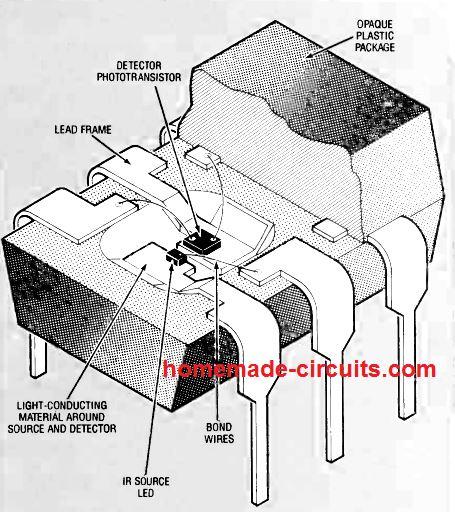
The above figure shows a dissected view of a typical six pin dual-in-line (DIP) optocoupler chip. When the terminals connected with the IR LED is supplied with an appropriate forward biased voltage it internally emits an infrared radiation in the wavelength of 900 to 940 nanometer range.
This IR signal falls on the adjacent photodetector which is normally an NPN phototransistor (having a sensitivity set in the identical wavelength), and it instantly conducts, creating a continuity across its collector/emitter terminals.
As can be seen in the image the IR LED and the phototransistor are mounted on adjacent arms of a lead-frame.
The lead-frame is in the form of stamping carved out from fine conductive sheet metal having several branch like finishing. The isolated substrates which is included to reinforce the device are created with the aid of the inner branches. The respective pinout of the DIP are correspondingly developed from the outer branches.
Once the conductive connections are established between the die case and the appropriate lead-frame pins, the space surrounding the IR LED and the phototransistor is sealed within an transparent IR supported resin which behaves like a "light pipe" or optical wave-guide between the two IR devices.
The complete assembly is finally molded in a light proof epoxy resin forming the DIP package. At the finish, the lead-frame pin terminals are neatly bent downward.
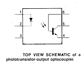
Optocoupler Pinout
The diagram above shows the pinout diagram of the typical optocoupler in DIP package. The device is also known as opto-isolator since no current is involved between the two chips, rather only light signals, and also because the IR emitter and IR detector feature a 100% electrically insulation and isolation.
The other popular names associated with this device are photocoupler or photoncoupled isolators.
We can see that the base of the internal IR transistor is terminated at pin 6 of the IC. This base is normally left unconnected since the main purpose of the devices is to couple the two circuits through an isolated internal IR light signal.
Likewise the pin 3 is an open or an unconnected pinout and is not relevant. It is possible to transform the internal IR phototransistor into a photodiode simply by shorting and connecting the base pin 6 with the emitter pin 4.
However, the above feature may not be accessible in a 4-pin optocoupler or multi channel optocouplers.
Optocoupler Characteristics
Optocoupler exhibit one very useful characteristic and that is its light coupling efficiency termed as current transfer ratio, or the CTR.
This ratio is enhanced with an ideally matching IR LED signal spectrum with its adjacent phototransistor detection spectrum.
CTR is thus defined as the ratio of output current to input current, at a rated bias level of a specific optocoupler device. It is represented by a percent:
CTR = Iced / If x 100%
When the specification suggests a CTR of 100% it refers to an output current transfer of 1 mA for each mA of current to the IR LED. Minimum values for the CTR may show variations between 20 to 100 % for different optocouplers.
The factors that may vary the CTR depends on the instantaneous specifications of input and output supply voltage and current to the device.
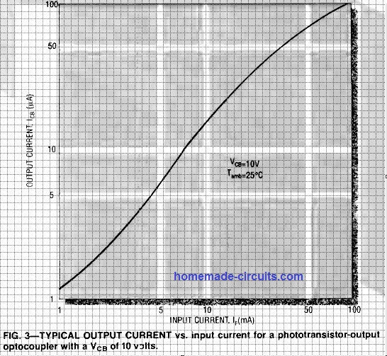
The figure above shows the characteristic plot of an optocoupler internal phototransistor's output current (ICB) vs. input current (IF) when a VCB of 10 V is applied across its collector/base pins.
Important OptoCoupler Specifications
A few of the essential optocoupler specification parameters can be studied from the below given data:
Isolation voltage (Viso): It is defined as the absolute maximum AC voltage that can exist across the input and output circuit stages of the optocoupler, without causing any harm to the device. The standard values for this parameter may fall between 500 V to 5 kV RMS.
VCE: it may be understood as the maximum DC voltage that could be applied across the device's phototransistor pinouts. Typically this may range between 30 to 70 volts.
If: It is the maximum continuous DC forward current that may flow in the IR LED or the IRED. It is the standard values of current handling capacity specified to a phototransistor output of the optocoupler, which may range between 40 to 100 mA.
Rise/fall time: This parameter defines the logical speed of the optocoupler response across the internal IR LED and the phototransistor. This may be typically from 2 to 5 microseconds for both rise and fall. This also tells us about the bandwidth of the optocoupler device.
Optocoupler Basic Configuration
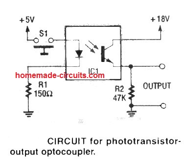
The figure above shows a basic optocoupler circuit. The amount of current that may pass through the phototransistor is determined by the applied forward bias current of the IR LED or the IRED, despite being entirely separated.
While the switch S1 is held open, current flow through the IRED is inhibited, which means no IR energy is available to the phototransistor.
This renders the device completely inactive causing zero voltage to develop across output resistor R2.
When S1 is closed, current is allowed to flow through the IRED and R1.
This activates the IR LED which begins emitting IR signals on the phototransistor enabling it to switch ON, and this in turn causes an output voltage to develop across R2.
This basic optocoupler circuit will specifically respond well to ON/OFF switching input signals.
However, if required the circuit can be modified to work with analog input signals and generate corresponding analog output signals.
Types of Optocouplers
The phototransistor of any optocoupler may come with many different output output gain and working specifications. The schematic I have explained below depicts six other forms of optocouplers variants which have their own specific combinations of IRED and output photodetector.
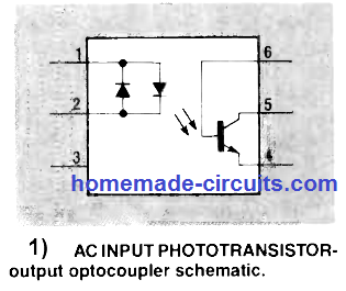
The first variant above indicates a bidirectional input and phototransistor output optocoupler schematic featuring a couple of back-to-back connected gallium-arsenide IRED's for coupling input AC signals, and also to safeguard against reverse polarity input.
Commonly this variant may exhibit a minimum CTR of 20%.
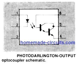
The next type above illustrates an opto-coupler whose output is enhanced with a silicon based photo-darlington amplifier. This allows it to produce higher output current compared to the other normal opto-coupler.
Due to the Darlington element at the output this type of optocouplers are able to produce a minimum of 500% CTR when the collector-to-emitter voltage is around 30 to 35 volts. This magnitude appears to be about ten times higher than a normal optocoupler.
However, these may not be as fast as the other normal devices and this may be a significant tradeoff while working with a photodarlington coupler.
Also, it may have a decreased amount of the effective bandwith by about a factor of ten. Industry standard versions of photoDarlington optocouplers are 4N29 to 4N33 and 6N138 and 6N139.
You can also get them as Dual and quad channel photodarlington couplers.
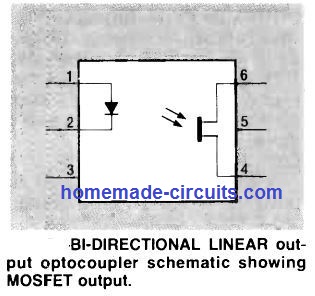
The third schematic above shows an optocoupler having an IRED and a MOSFET photosensor featuring bi-directional linear output. The isolation voltage range of this variant can be as high as 2500 volts RMS. The breakdown voltage range can be within 15 to 30 volts, while the rise and fall times is around 15 microseconds each.
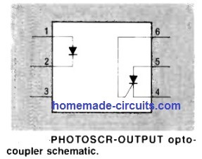
The next variant above demonstrates a basic SCR or thyristor based opto photosensor. Here the output is controlled through an SCR. The isolation voltage of OptoSCR type of couplers is typically around 1000 to 4000 volts RMS. It features a minimum blocking voltages of 200 to 400 V. The highest turn ON currents (Ivr) can be around 10 mA.
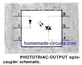
The image above displays an optocoupler having a phototriac-output. These kind of Thyristor based output couplers generally feature a forward blocking voltages (VDRM) of 400 V.
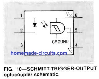
Optocouplers featuring Schmitt trigger property are also available. This type of optocoupler is displayed above that includes a IC based optosensor having a Schmitt trigger IC that will convert a sine wave or any form of pulsed input signal into rectangular output voltage.
These IC photodetectors based devices are actually designed to work like a multivibrator circuit. Isolation voltages may range between 2500 to 4000 volts.
Turn-on current is usually specified between 1 to 10 mA. The minimum and maximum working supply levels are between 3 to 26 volts, and the maximum speed of data rate (NRZ) is 1 MHz.
Application Circuits
The internal functioning of optocouplers is exactly similar to the working of an discretely set up IR transmitter and receiver assembly.
Input Current Control
Just like any other LED, the IR LED of an optocoupler also needs a resistor to control the input current to safe limits. This resistor can be connected in two basic ways with the optocoupler LED, as demonstrated below:
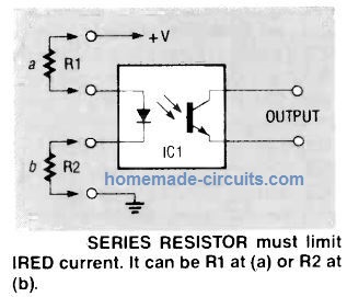
The resistor can be added in series either with the anode terminal (a) or cathode terminal (b) of the IRED.
AC Optocoupler
In our earlier discussions I have explained that for AC input, the AC optocouplers is recommended. However, any standard optocoupler can be also safely configured with an AC input by adding an external diode to IRED input pins as proven in the following diagram.
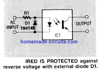
This design also ensures safety for the device against accidental reverse input voltage conditions.
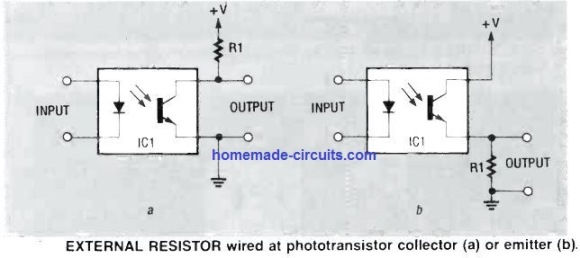
Digital or Analogue Conversion
In order to get a digital or analogue conversion at the output of the optocoupler, a resistor can be added in series with the optotransistor collector pin or the emitter pin respectively, a shown below:
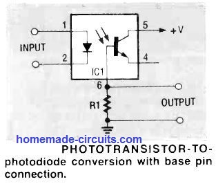
Converting to Photo-Transistor or Photo-Diode
As indicated below, an regular 6-pin DIP optocoupler's output photo-transistor can be converted to a photo-diode output by connecting the transistor's base pin 6 of its photo-transistor with ground, and by keeping the emitter unconnected or shorting it with pin6.
This configuration causes a significant increase in the rise time of the input signal, but also results in a drastic reduction in the CTR value down to 0.2%.
Optocoupler Digital Interfacing
Optocouplers can be excellent when it comes to digital signal interfacing, operated at various supply levels.
Optocouplers can be used for interfacing digital IC's across identical TTL, ECL or CMOS family, and likewise across these chip families.
Optocouplers are also the favorites when it comes to interfacing personal computers or microcontrollers with other mainframe computers, or loads like motors, relays, solenoid, lamps etc. The below shown diagram illustrates the interfacing diagram of an opto-coupler with TTL circuits.
Interfacing TTL IC with Optocoupler
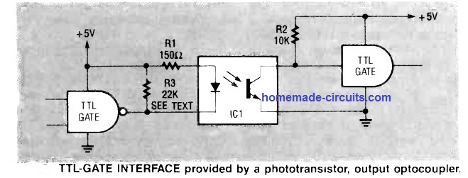
Here we can see that IRED of the optocoupler is connected across the +5V and the TTL gate output, instead of the usual way which is between the TTL output and ground.
This is because the TTL gates are rated to produce very low output currents (around 400 uA), but are specified to sink current at a fairly high rate (16 mA). Therefore the above connection allows optimal activation current for IRED whenever the TTL is low. However this also means the output response will be inverted.
Another drawback that exists with TTL gate output is that, when its output is HIGH or logic 1, might produce around a 2.5 V level, which might not be enough to switch OFF the IRED fully. It must be at least 4.5 V or 5 V to enable complete switch OFF of the IRED.
To correct this issue, R3 is included which makes sure the IRED shuts off completely whenever the TTL gate output turns HIGH even with a 2.5 V.
The collector output pin of the optocoupler can be seen is connected between the input and ground of the TTL IC. This is important because a TTL gate input must be adequately grounded at least below 0.8 V at 1.6 mA to enable a correct logic 0 at the gate output. It must be noted that the set up shown in the above figure allows a non-inverting response at the output.
Interfacing CMOS IC with Optocoupler
Unlike TTL counterpart, CMOS IC outputs have the ability to source and sink sufficient currents magnitudes up to many mAs without an issue.
Therefore, these IC's can be easily interfaced with optocoupler IRED either in the sink mode, or source mode as shown below.
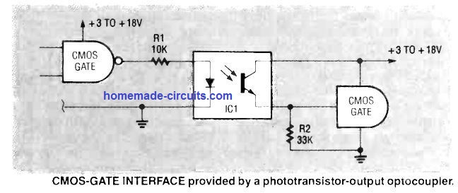
No matter which configuration is selected at the input side, R2 at the output side must be sufficiently large to enable a full output voltage swing between logic 0 and 1 states at the CMOS gate output.
Interfacing Arduino Microcontroller and BJT with Optocoupler
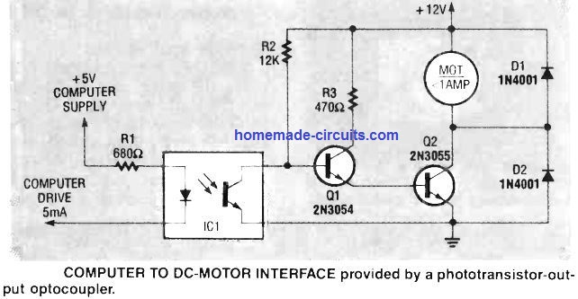
The above figure shows how to interface a microcontroller or Arduino output signal (5 volts, 5 mA) with a relatively high current load through an optocoupler and BJT stages.
With a HIGH +5V logic from the Arduino, the optocoupler IRED and phototransistor both remain switched off, and this allows Q1, Q2 and the load motor to remain turned ON.
Now, as soon as the Arduino output goes low, the optocoupler IRED activates and turns ON the phototransistor. This instantly grounds the base bias of Q1, switching OFF Q1, Q2 and the motor.
Interfacing Analogue Signals with Optocoupler
An optocoupler can be also effectively used for interfacing analog signals across two circuit stages by determining a threshold current through the IRED and subsequently modulating it with the applied analog signal.
The following figure shows how this technique may be applied for coupling an analogue audio signal.
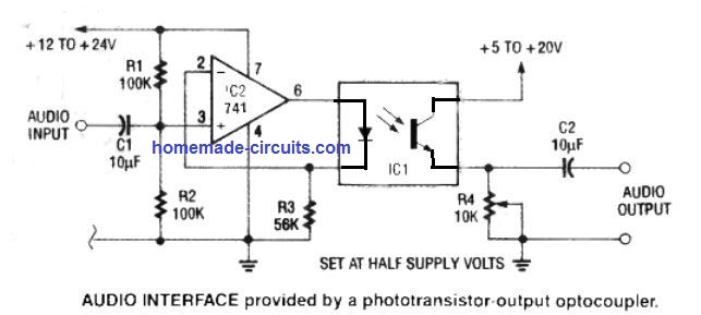
The op amp IC2 is configured like a unity gain voltage follower circuit. The IRED of the opto-coupler's can be seen rigged to the negative feedback loop.
This loop causes the voltage across R3 (and therefore the current through the IRED) to precisely follow, or track the voltage that's applied to pin#3 of the op amp, which is the non-the inverting input pin.
This pin3 of the is op amp set up at half the supply voltage via R1, R2 potential divider network. This allows the pin3 to be modulated with an AC signals which can be an audio signal and causes the IRED illumination to vary as per this audio or the modulating analogue signal.
The quiescent current or the idle current draw for the IRED current is attained at 1 to 2 mA via R3.
On the output side of the optocoupler the quiescent current is determined by the phototransistor. This current develops a voltage across potentiometer R4 whose value needs to be adjusted such that it generates a quiescent output which is also equal to the half the supply voltage.
The tracking modulated audio-output signal equivalent is extracted across potentiometer R4, and decoupled through C2 for further processing .
Interfacing Triac with Optocoupler
Optocouplers can be ideally used for creating a perfectly isolated coupling across a low DC control circuit and a high AC mains based triac control circuit.
It is recommended to keep the ground side of the DC input connected to a proper earthing line.
The complete set up can be viewed in the following diagram:
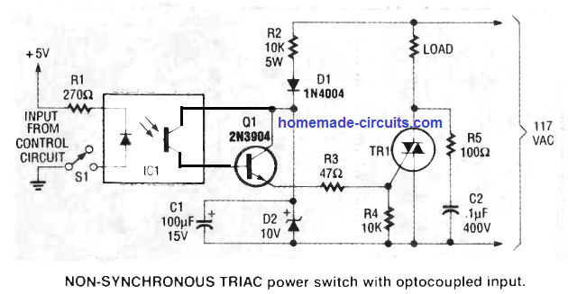
The above design can be used for an isolated control of mains AC lamps, heaters, motors and other similar loads. This circuit is not zero crossing controlled set up, meaning the input trigger will cause the triac to switch at any point of the AC waveform.
Here the network formed by R2, D1, D2 and C1 create a 10 V potential difference derived from the AC line input. This voltage is used for triggering the triac through Q1 whenever the input side is switched ON by closing the switch S1. Meaning as long as S1 is open the optocoupler is off due to a zero base bias for Q1, which keeps the triac switched OFF.
The moment S1 is closed it activates the IRED, which switches ON Q1. Q1 subsequently connects the 10 V DC to the gate of the triac which switches the triac ON, and eventually also switches ON the connected load.
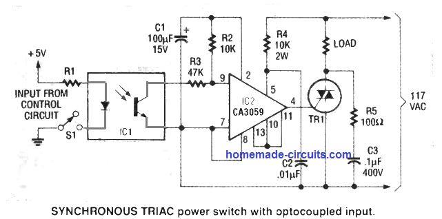
The next circuit above is designed with a silicon monolithic zero-voltage switch, the CA3059/ CA3079. This circuits allows the triac to trigger synchronously, that is only during the zero voltage crossing of the AC cycle waveform.
When S1 is pressed, the opamp responds to it only if the triac input AC cycle is near a few mV near the zero crossing line. If the input trigger is made while the AC is not near the zero crossing line, then the op amp waits until the waveform reaches the zero crossing and only then triggers the triac via a positive logic from its pin4.
This zero crossing switching feature safeguards the connected from sudden huge current surge and spike, since the turn ON is done at the zero crossing level and not when the AC is at its higher peaks.
This also eliminates unnecessary RF noise and disturbances in the power line. This optocoupler triac based zero crossing switch can be effectively used for making SSR or solid state relays.
PhotoSCR and PhotoTriacs Optocoupler Application
Optocouplers having their photodetector in the form of photoSCR and photo-Triac-output are generally rated with lower output current.
However, unlike other optocoupler devices, optoTriac or optoSCR feature a rather high surge current handling capacity (pulsed) which may be much higher than their rated RMS values.
For SCR optocouplers, the surge current specification may be as high as 5 amps, but this can be in the form of a 100 microsecond pulse width and a duty cycle no more than 1%.
With triac optocouplers, the surge specification may be 1.2 amps, which must last only for 10 microsecond pulse with a maximum duty cycle of 10%.
The following images show a few application circuits using triac optocouplers.
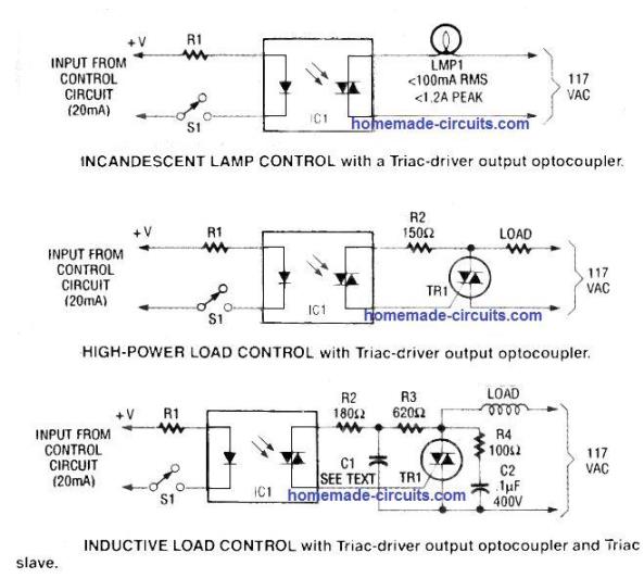
In the first diagram, the photoTriac can be seen configured to activate the lamp directly from the AC line. Here the bulb must be rated at less than 100 mA RMS and a peak inrush current ratio lower than 1.2 amps for safe working of the optocoupler.
The second design shows how the photoTriac optocoupler can be configured for triggering a slave Triac, and subsequently activating a load as per any preferred power rating. This circuit is recommended to be used only with with resistive loads such as incandescent lamps or heater elements.
The third figure above illustrates how the upper two circuits could be modified for handling inductive loads like motors. The circuit consists of R2, C1, and R3 that generate a phase shifting on the gate drive network of the Triac.
This allows the triac to go through a correct triggering action. Resistor R4 and C2 are introduced as a snubber network to suppress and control surge spikes due to inductive back EMFs..
In all the above applications, R1 must be dimensioned such that the IRED is supplied with at least 20 mA forward current for proper triggering of the triac photodetector.
Speed Counter or RPM Detector Application
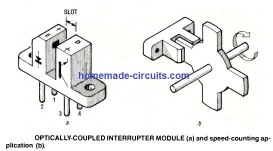
The above figures explain a couple of unique customized optocouplers modules which could be used for speed counter or RPM measurement applications.
The first concept shows a customized slotted coupler-interrupter assembly. We can see a slot in the form of an air gap is placed between the IRED and the phototransistor, which are mounted on separate boxes facing each other across the air gap slot.
Normally the Infrared signal is able to pass across the slot without any blockage while the module is powered. We know that infrared signals can be totally blocked by placing an opaque object in its path. In the discussed application when an obstruction like wheel spokes is allowed to moved through the slot, causes interruptions to the passage of the IR signals.
These subsequently get converted to clock frequency across the output of the phototransistor terminals. This output clock frequency will vary depending on the speed of the wheel, and could be processed for the required measurements. .
The indicated slot may have a width of 3 mm (0.12 inch). The phototransistor used inside the module has a phototransistor should be specified with a minimum CTR of about 10% in the "open" condition.
The module is actually a replica of a standard optocoupler having an embedded IR and a photoransistor, the only difference is, here these are discretely assembled inside a separate boxes with an air gap slot separating them.
The first module above can be used for measuring revolution or like a revolution counter. Each time wheel tab crosses the slot of the optocoupler, the phototransistor switches OFF generating a single count.
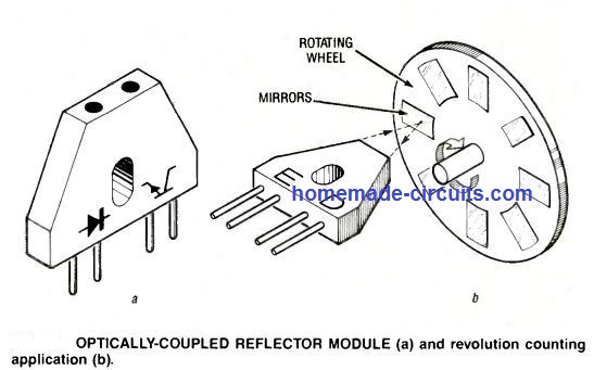
The attached second design shows optocoupler module designed to respond to reflected IR signals.
The IRED and the phototransistor are installed in separate compartments in the module such that normally they cannot "see" each other. However the two devices are mounted in such a way that both share a common focal point angle that's 5 mm (0.2 -inch) away.
This enables the interrupter module to detect nearby moving objects which cannot be inserted in thin slot. This type of the reflector opto module can be used for counting the passage of large objects over conveyor belts or objects sliding down a feed tube.
In the second figure above we can see the module being applied as a revolution counter which detects the reflected IR signals between the IRED and the phototransistor through the mirror reflectors mounted on the opposite surface of the rotating disk.
The separation between the optocoupler module and the spinning disk is equal to the 5 mm focal length of the emitter detector pair.
The reflective surfaces on the wheel can be made using metallic paint or tape, or glass. These customized discrete optocouplers modules could be also effectively applied for engine shaft speed counting, and engine shaft RPM or rotation per minute measurement etc. The above explained Photo interrupters and photoreflectors concept can be built using any opto detector device such as a photodarlington, photoSCR, and photoTriac devices, as per the output circuit configuration specifications.
Door/Window Intrusion Alarm
The above explained optoisolator interrupter module can be also effectively as a door or window intrusion alarm, a shown below:
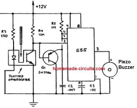
This circuit is more effective and easier to install than the conventional magnetic reed relay type intrusion alarm.
Here the circuit utilizes a IC 555 timers as a one shot timer for sounding the alarm.
The air gap slot of the optoisolator is blocked with a lever kind of attachment, which is also integrated to the window or the door.
In an event the door is opened or the window is opened, the blockage in the slot is removed, and the LED IR reaches the phototransistors and activates the one shot monostable IC 555 stage.
The IC 555 instantly triggers the piezo buzzer alerting regarding the intrusion.
Different Families of Optocouplers
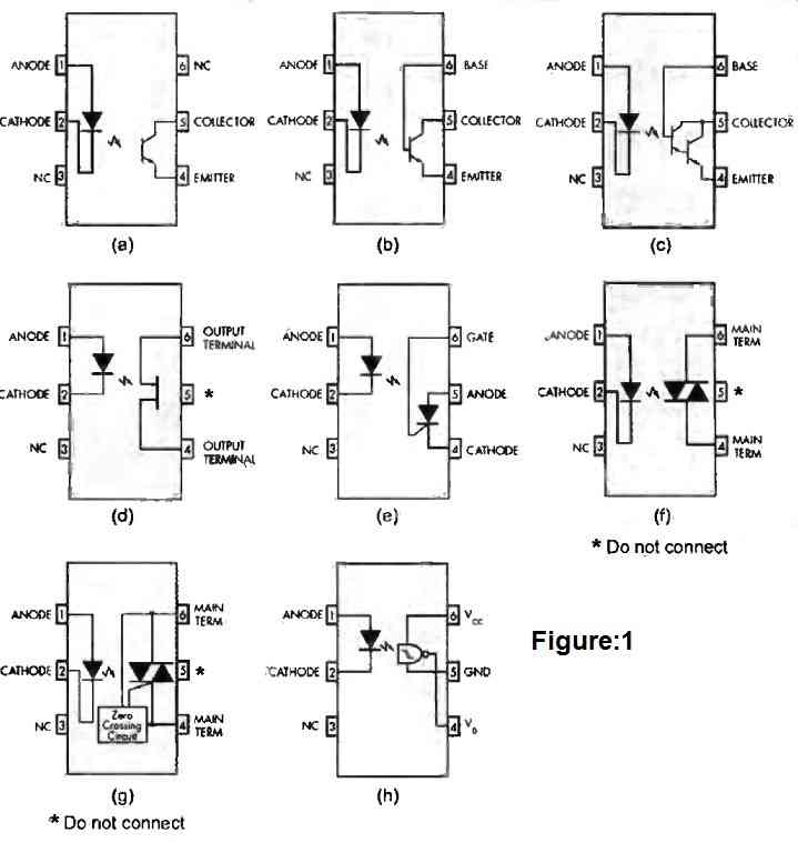
Figure 1 above presents the pinouts that are most familiar for the main families of optocouplers in DIP6 packages, whose output stage was initially a photodiode or a phototransistor.
Diversity then emerged with output stages using Darlington, thyristor, and triac. More recently, other optocouplers have been specifically designed for logic interfaces.
Characterized by a low input current, generally less than 1.6 mA, they have a Schmitt trigger logic output stage and a direct power supply circuit compatible with TTL or CMOS (Figures 3h and 4c).
Thus, these new optocouplers are compatible with logic circuits both as inputs and outputs. Other generations of optocouplers have since been developed to meet specific applications.
Optocouplers with Transistor Output
These are popularly called "optotransistor", the output stage is a phototransistor. These optotransistors represent the majority of optocoupler production. When a current passes through the infrared LED (IRED), infrared light irradiates the base-collector junction of a photosensitive transistor. The light energy is then converted into current, which is amplified by the transistor's gain or the hFE.
The current transfer ratio of an optotransistor
The ratio of the phototransistor collector current to the IRED bias current, is generally between 10% and 500% for the latest models. Some models have an output pin connected to the phototransistor's base (Figure 2b).
This connection can be used for specific applications, but mainly to improve the dynamic behavior of the output and primarily to reduce signal distortion.
To do this, a resistance of around 100 kΩ to 300 kΩ is used to tie the transistor's base to ground to improve the discharge of the parasitic capacitances of the phototransistor junctions. This improves the switching speed of the output, particularly the turn-off duration is reduced.
Optocouplers with Darlington output
Commonly called "optodarlington", the output stage of this optocoupler is a photodarlington whose operation is similar to that of the optotransistor previously described (Figure 1c). However, its transfer ratio is much better and can reach 1,000%, with a guaranteed minimum ratio of 100%.
On the other hand, it is less fast.
Optocouplers with Thyristor output
This optocoupler, or more commonly "optothyristor", is an optocoupler whose photodetector is a photosensitive thyristor (Figure 1e). These optocouplers have been designed for controlling "AC mains" applications involving important isolation safety measures.
Optocouplers with Triac Output
Optotriacs have become very popular and are commonly used for interfaces between a logic circuit and a "AC mains" application.
There are two main types of optotriacs. One has a classic behavior with the phototriac triggering as soon as enough current passes through the IRED.
The other allows triac triggering at the zero crossing of the sector voltage. This feature is very valuable as it avoids current spikes and limits AC interference.
It allows for a progressive growth of current in the load, which is a "plus" for heating resistors, as they have a lower resistivity when cold.
Logic Output Optocouplers
Initially, fairly fast optocouplers were developed, such as models like H11L1/2 or M005007/8/9, with rise and fall times, t On and t Off, less than 4 ps (figure 1h). Their output stages are often composed of a very fast integrated detector with Schmitt trigger, requiring a stable power supply ranging from 3 to 15 V depending on the application. Their outputs are generally open collector.
Later, very fast optocouplers were made allowing switching speeds of around 10 Mbd. The output stage is an integrated detector, requiring an external power supply, usually +5 V for the fastest models.
The output is often an NMOS transistor with open drain. An "Enable" input for blocking the output is often present and forces the output, depending on the model, to a "high" state or to a high impedance state. The pinout of this new generation of optocouplers is not universal and varies from one manufacturer to another.
Among different brands, Vishay presents logic output optocouplers in DIP8 packages, whose pinout is similar to that of an optotransistor in a DIP6 package. Thus, it is possible to use such a DIP6 package instead of a Vishay DIP8 optocoupler with logic output. Double versions in DIP8 package are also available.
References
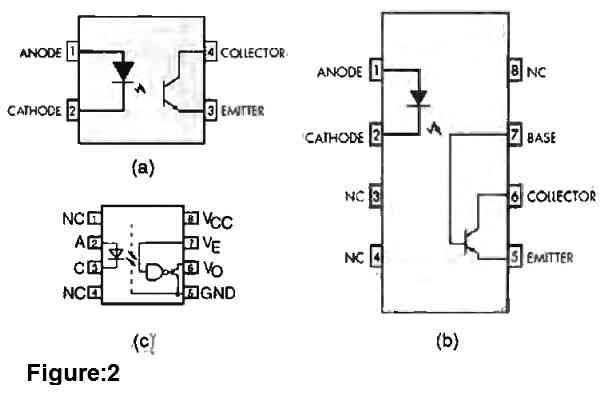
In addition to the increasingly diverse range of optocouplers, many models have been manufactured over time. To meet multiple applications, other pinouts exist, particularly for DIP4 or DIP8 packages with pinouts similar to those of popular DIP6 packages (figure 2).
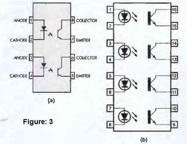
Moreover, some models combine several optocouplers with independent inputs/outputs in the same package (figure 3). Some variants exist, particularly with a reversal of pinout between the emitter and the collector of the phototransistor.
A diode can also be present in anti-parallel on the IRED of the input stage to protect against reverse voltage when the power source is alternating (figure 4 below).
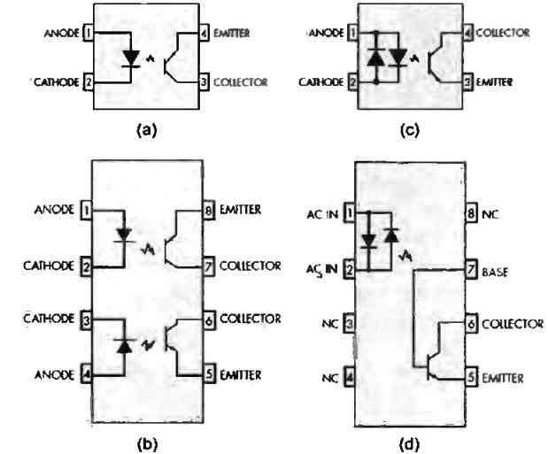
Of course, these different models also exist in Darlington or FET versions. The wide variety of references makes a detailed synthesis of the characteristics of the main models laborious.
Creating Basic Logical Functions using Optocouplers
Various logical functions can be realized using optotransistors. The output of these logical functions can be compatible with TTL or CMOS depending on the value of the power supply voltage associated with the output stage of the optocouplers.
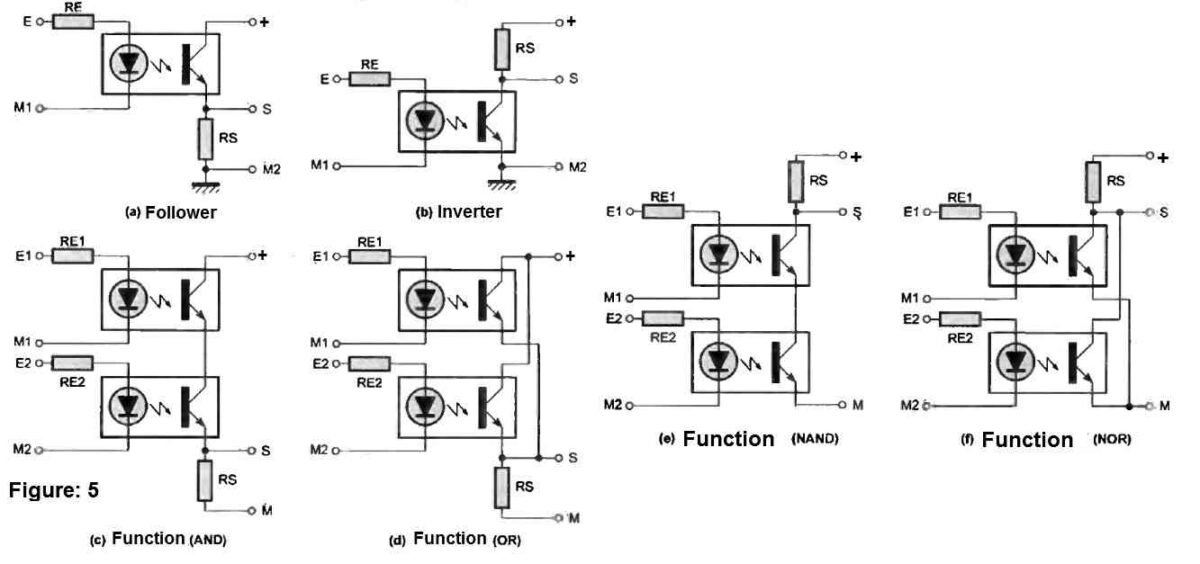
Figure 5a shows a non-inverted logical connection. In the absence of voltage on the input (E), the photo-transistor of the output stage is blocked and the output (S) is in the "low" state due to the resistance RS.
On the other hand, the presence of voltage on the input (E) causes the photo-transistor to conduct. For suitable values of the resistors RE and RS, the photo-transistor will be saturated and the power supply voltage Valim will appear at the output (S).
An inverted connection is obtained by placing the resistor RS between the collector of the photo-transistor and the power supply Valim (figure 5b).
Using two optotransistors, logical functions AND, OR, NAND, NOR can be wired.
The AND and NAND functions are obtained by placing the output stage of the photo-transistors in series. Thus, the resistor RS will only be traversed by a current if both photo-transistors are conductive, i.e., if both inputs (El) and (E2) are active (figures 7c and 7e).
The OR and NOR functions are implemented by wiring the output stage of the two optocouplers in parallel (figures 7d and 7f). Thus, if at least one of them is conductive, the logical state of the output will be switched. Another advantage is that the voltage sources (El) and (E2) can be isolated or have a common ground.
Similarly to the implementation of "Follower" and "Inverter" connections, the inversion of the OR and AND functions is obtained by placing the load resistor at the output, either connected to ground or to the power supply positive.
RS flip-flop
A brief pulse on the input (S) is sufficient to switch the output (Q) of this flip-flop to the "high" state. Resetting this output (Q) is achieved by applying a pulse on the input (R). The timing diagrams in Figure 6 illustrate this operation.
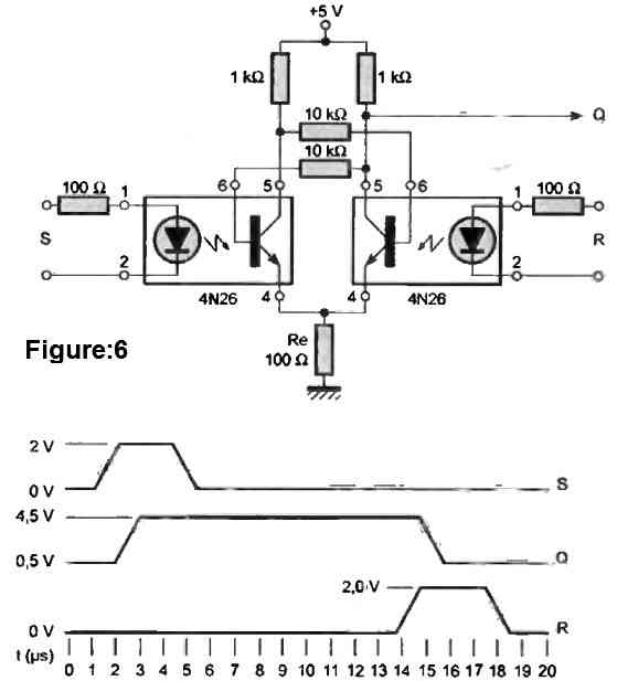
One of the particularities of this circuit is the use of optocouplers, whose output stage has a third connection connected to the base of the phototransistor. This application illustrates one of the utilities of this optional connection.
Monostable
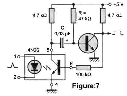
A monostable function is obtained with the circuit of Figure 7. A brief input pulse will trigger a "stable high" state momentarily at the output, whose duration is proportional to the time constant R x C. This configuration essentially aims to extend the duration of the pulse applied to the input of the optocoupler.
Audio connection
Although mainly designed to transmit a logic level, optocouplers can be used for audio applications (figure 8).
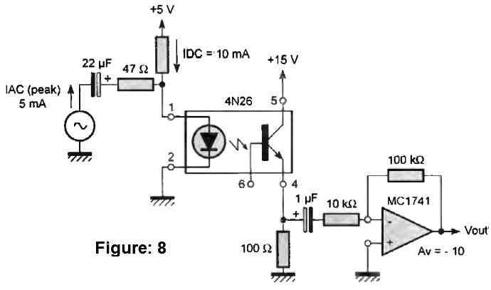
In this case, the phototransistor operates in linear mode, not saturated and in order to limit distortion of the audio signal, the DC bias current of the IRED must place the operating point at the center of a linear portion of the IRED characteristic.
Choice of RE and RS resistors
In typical application examples of optocouplers in Figure 5, the RE and RS resistors correspond respectively to the input current calibration resistor RE and the output discharge resistor RS. These resistors are systematically determined in various applications involving optocouplers.
Calculation of RE
For use as a switch with an optocoupler, the resistance RE should be sufficiently low to ensure that the current in the IRED is sufficient. For general use optocouplers, a current of approximately 5 to 10 mA is suitable. In this case, the value of the resistance RE is calculated from the level of the voltage applied to the optocoupler.
For a voltage source of +5 V and an IF current of 10 mA, the calculation becomes:
RE = (5 - VF) / 0.01.
VF is the forward voltage drop across the IRED, which is approximately 1.1 V to 1.5 V. Therefore, a resistance of 330 ohms is suitable.
Calculation of RS
In order for the phototransistor to be sufficiently saturated, its load resistance RS should have a minimum value RS(min), dependent on the value of the supply voltage and the current transfer ratio between the input and the output.
Older technical documentation provided a curve indicating the value of the phototransistor's collector current Ic as a function of the current IF passing through the IRED (Figure 9 below).
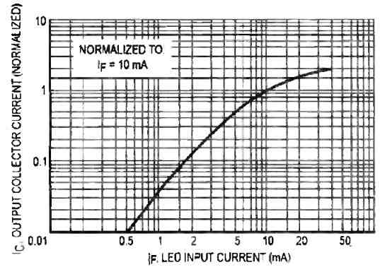
More recent documentation provides the CTR ratio, the ratio between the output current and the input current of the optocoupler.
Two ratios are established depending on the operating mode of the optocoupler. These are the saturation CTR and the linear CTR.
In saturation mode, the CTR ratio often decreases beyond an optimal value of the current IF (Figure 10).
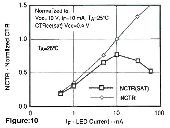
These two ratios, CTR(sat) and CTR, are defined in saturation mode for a VCE generally of 0.4 V and in linear mode for a VCE of +5 or +10 V, depending on the manufacturers.
The value of the resistance RS is given by the following expression:
RS(min) = (Vsupply - 0.4)/(CTR x IF - IL)
For example, for a transfer ratio of 12%, an IF current of 10 mA, a +5 V power supply, and an HCMOS logic with IL = 50 pA, the calculation becomes:
RS(min) = 4.6/(0.12 x 0.01 - 50 x 10-6)
So RS(min) = 4.0 kΩ.
The value of RS should be at least 4 times the collector current Ic. Therefore, a resistance of 4.7 kΩ should be used, knowing that the optocoupler switching will be faster with a lower RS resistance

Questions & Answers
Hi Swagatam,
This is a brilliant reference. Very very informative, easy to read, easy to understand (although will need to read a few times to digest fully).
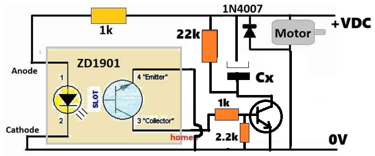
I am back on the quest for control of a 12V DC motor. My input is an intermittent (randomly on for 5 to 20 seconds) 20V supply which I am reducing to 10V (as 12V is too fast for my needs). When the input power drops, I need the motor to complete its current revolution. I have an optical interrupter that has its beam cut at 0 degrees rotation. So, I am assuming a capacitor is to be used to keep the motor turning, the opto to ground the motor when the beam is cut, and also assuming I need a diode to stop current flowing back from the motor and blowing my power regulator? The opto also needs to be disabled so it allows the motor to turn when the next input starts.
I can get the opto to ground the motor. I can get the capacitor to keep the motor turning. I cannot get the opto to work correctly when the input drops and the capacitor is discharging. I have not tested it but just assume the diode should go between the input from the voltage regulator and this circuit?
If you can help out with this it would be appreciated.
Hi Swagatam,
We did go through some options which included eventually using a 555 to limit the number of revolutions. I kept blowing up 4017ICs and was unable to get a suitable solution working. I also tried a stepper motor option but failed with that. I subsequently simplified the module connected to the motor so all is needed is for the motor to start when the input starts and stop when the opto (at 0 degrees) is blocked by a cam on the motor driveshaft which will happen within a single revolution after the input power drops. So basically now the design is that the motor is connected directly to the input so it starts immediately the input comes on. When the input drops, the capacitor should discharge to the motor until the opto beam is blocked which should ground the motor so it immediately stops. This is a simpler overall design than I was working on.
I have reset and started with this circuit “motor-control-using-photo-interruptor.jpg” but removed the +5V pulse which was a trigger. I am trying to feed the capacitor discharge back through the motor with the opto switching on a ground connection between the capacitor and the motor. The opto only needs to be “ON” when the input drops so its connected to the capacitor (-) pole and the optos CE go to the TIP122 which grounds the motor when the beam is blocked. Does this make sense? Or am I looking at it wrongly?
…The image mistakenly shows incorrect collector/emitter orientation for the opto transistor. Please make sure to swap the emitter/collector ppins of the opto transistor, meaning the emitter should go to the 1k resistor and the collector to the positive supply.
Hi Swagatam,
Ok. Thanks and I understand both points made. I am having trouble applying your IC555 concept in my head though. I envisage one more capacitor to keep power to the IC and once drains back through the motor? And somewhere in the design, power off will change the output from the 555?
Cheers
No problem Michael,
Actually there’s no need of a 555 circuit, it can be actually done with a very simple idea.
Please try the following concept, this will nail it.
Let me know how it goes:
Thank you Michael,
Yes it makes sense.
According to me the design should look something like this:
Thanks Swagatam.
Yep easy enough to follow. I was still using two TIPs and I think the switching was flip-flopping or something like that…
Can I put a diode on the +ve side of the capacitor? Am I correct that when the power goes off the capacitor is essentially discharging to itself? And to stop any surge back to the power source should I have a diode there?
No problem, Michael!
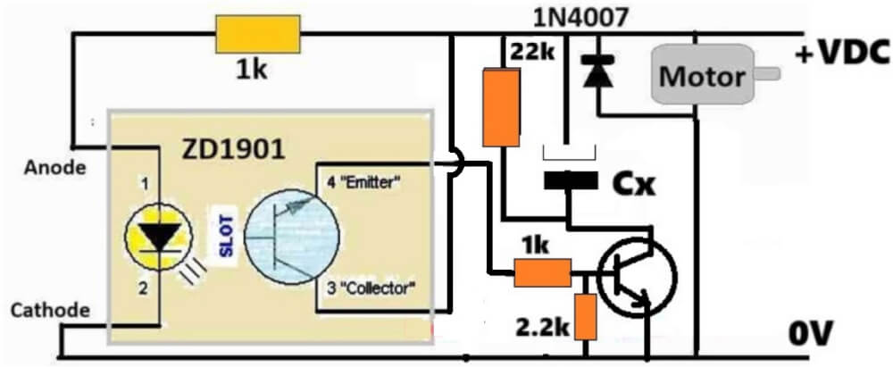
The capacitor already has a 22k resistor for discharging, so a diode may not be required. You can tweak the 22k value to some lower levels for faster discharging, if required.
Once the transistor cuts off the capacitor’s negative pin, it cannot discharge through anything, except the 22k resistor.
Hi Swagatam,
I am doing something wrong I think. What type of transistor do you recommend. It appears that the discharging config for the capacitor is not working. If I cut the power the motor stops immediately even when I am using 470uF. I also swapped out the motor for a LED and it also goes off as soon as the power drops. I would think that an LED would fade even if the motor stops.
Hi Michael,
Please replace the transistor with a diode 1N4007 (cathode to ground, anode to capacitor’s negative) and check the LED response. If this does not cause fading effect on the LED, that would mean the transistor concept won’t work, instead the device will need to be replaced with a non-polar device…..in that case we will need an IC based controller such as IC 555 or an op-amp…
Hi Swagatam,
I return bearing sad news 🙁
So, I replaced the transistor as you mentioned as well as changing the resistor and capacitor values and I still get no fading effect on the LED just a simple on/off response. I was really after that kind of simplicity. Anyway I was thinking also could the functional limits (minimum current/voltage) of the opto have something to do with that circuit design not working as intended?
A thought though … I am using a TIP122 which is a NPN type. If the power dropping effectively triggers the capacitor discharge then would it be better to have some configuration around a PNP (TIP127 ?? right)?
Interested in how an IC555 solution would look.
Thanks
Thanks for the update Michael, sorry it did not work.
When you replace the transistor with a diode, the opto is isolated, so has no role to play, so the opto might not be the issue.
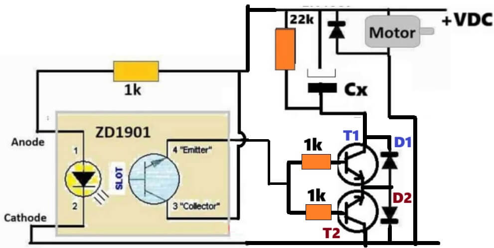
Our concept did not work, because I think the capacitor requires a bidirectional switching to be used in series with it to ensure it is able to charge through one direction and subsequently discharge through the reverse direction.
If my assumption is true, then I think the following modification should definitely work. Now the capacitor can charge through T1, D2, and then discharge through T2, D1. Sorry, I could not understand your suggestion regarding the incorporation of an PNP device? A 555 output also employs a bidirectional source, so it can be also used for this application, I guess….
Thanks Swagatam.
I have built this twice using different breadboards (due to previous dubious boards) as well as to check how I was connecting everything. Same issue and do not understand why. I can see it should work as expected. I am using TIP122 transistors, a 470uF cap. It’s a 12V motor with same supply. Resistors as detailed in the design. Should T2 be a TIP127? Swapped the motor for an LED and also no fade out.
Hi Michael,
The configuration will not work in the given conditions, because for any bidirectional switch to work, the transistor emitters and the bases must be switched with an isolated supply, which is not happening in my proposed design and is not possible here. I realized this immediately and I informed you about this in the subsequent email, maybe you did not see it.
Using a PNP for T2 will not work in this circuit because in bidirectional switch both the devices needs to have identical polarity. If you are thinking about a push-pull NPN/PNP combination circuit, even won’t work here correctly.
Only using a 555 IC seems to provide some hope.
Let me know your opinion.
Hi Michael, sorry again, the bidirectional concept might not be applicable here because here the optocoupler trigger source to the BJTs needs to be isolated from the motor supply…which might not be feasible here because the grounds of the opto and the motor are joined in common.
If you want I can try designing the 555 version for this application.
Thank you Michael,
Glad you found the post helpful.
Regarding your current application, i think we have discussed this earlier, and i had tried to solve it through subsequent circuit diagrams.
Can you please check the following post, which has all the details of our earlier discussions in the COMMENTS section. Please let me know if I am wrong.
https://www.homemade-circuits.com/
Hi Dear Swagatam;
There are 4 optocouplers on my TV power board. Multimeter is on the diode mode and three of them show the value of 1.080V but one of the optocouplers shows the value as about 0.800. Is that issue should I remove and then measure it or that may be normal? Thanks in advance
Hi Suat,
The value shows the forward voltage drop of the opto LED.
You can remove the opto from the PCB and check again.
However checking it physically by supplying voltage to the LED side and testing the transistor conduction will provide more accurate results.
Thank you Swagatam, I have forgotten the one important point that: it shows the value 0.8V in both direction I mean when I change the side of the probes then I see the same value.
Thank you Suat, if you are getting this reading after removing the opto from the PCB, then definitely the opto is faulty.
Hi Mr Swagatam;
Is it possible to use 4N25 instead of opto-coupler 817 type which is being used on the battery charger circuit.
Hi Suat,
Yes, both the optos are interchangeable with each other.
Good day Sir, please I need a guide. How can I connect an ac signal to boost another low ac input
Hello Tinu, AC signal can be boosted using a transformer not through an opto coupler
Please how can I use optocoupler to isolate 96v input, I can only do for 24v,.
Thanks Swag
Seun, please explain what exactly are you trying to implement, I will try to figure it out
I have a circuit I used to isolate to 2 DC systems of 24v but I want to upgrade the systems to 48v and 96v respectively.
Maybe this article will help you to configure the optocoupler accordingly
https://www.homemade-circuits.com/how-to-drive-relay-through-opto-coupler/
Will you please end me a pdf copy of this article I found it very good for eduactional purposes. I tech at a Technical high-school in Mexico
Thank you, and glad you liked the post! However I am sorry, I have no idea how this article may be converted to a pdf copy
Hi, I am hopeful that you will be able to suggest a circuit that will provide an isolated potentiometer that I can use to replace a 4.7K pot used to control the speed of a DC motor. The current motor circuit board runs a bench top milling machine that has a 90V motor. The pot controls the variable speed using 12V.
I have a PC that can output 0-10V that I would like to use to control the spindle speed. I wondered if an optocoupler circuit could achieve this setup with your help?
Hi, it can be probably achieved through an LED/LDR optocoupler which will need to built manually by enclosing an LDR ad an LED face to face inside a light proof tube.
The LED terminal then could be applied with the 0-10V supply via a 1k resistor, and the resistor could then be used in place of the 4k7 preset
You have helped us in the past, and we greatly appreciated it.
We are now looking for an optocoupler with an AC input and AC output. We want to be able to select, through jumpers, a high or low 24VDC signal for input and/or output. We have searched and searched, but can find only AC input with DC output (ILD755-1), or DC input with AC output (IL420).
Thank you very much for your help.
Louis
Glad I could help! I think IL420 can be used with AC input if the AC is rectified through a bridge rectifier, which will enable both the half cycles to be detected by the input LED and this will correspondingly processed by the output side triac.
Thank you, Swagatam. Do you know of an optocoupler with an AC input and Triac output? There is simply not enough board space to add a separate Triac. I lhave been unable to find a combined unit. Again, we appreciate your help.
Louis
You are welcome Loius, sorry I searched for it but couldn’t find any.
Există ansamblu de optocuplor cu fantă de 4 biți ?
(4 optocuplori montați pe un singur bloc)
Dear mr Swag
Thank you so much for your reply which didn’t take time.
please how can i purchase any of the sensors you mentioned in the above either optocoupler or IRLED module?.Do you have them?
Thanks.
Thanks Mr Patrick, You can probably buy them from any online electronic spare part store
Hi sir, Please provide how to test Pc410L and pC457L OPIC photocoupler
Hi Anand, you can test it through the following set up:
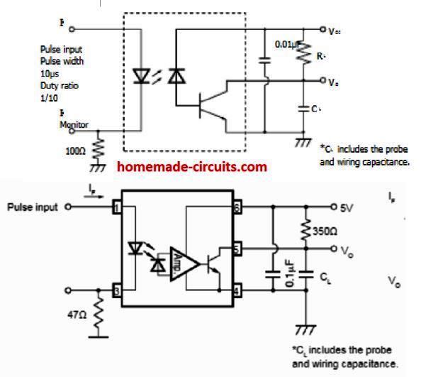
when input pulse is ON, the output Vo will be zero and vice versa
excuse me sorry for my poor english
i mean,i want turn on triac among 0 to 360 degree
from the ac input voltag to obtain different voltages
as you said i want a optocopler that is not having cross detector
because cross detector is barrier my purpose
dear sir if i want to controling input voltage for example the single phase ac motor with the train pulses that i control via atmega 32
i connected output micro to input of the moc 30 63
tank you in advance
Hi Sedigh,
for controlling AC motor with triac and PWM, zero crossing becomes very important to avoid triac failure and damage. Moreover, zero crossing will not affect the control procedure of the motor with the pulse train. This kind of control is called zero voltage switching and can be effectively done even with a zero crossing detection.
However for a smooth 0 to 360 degree control you can try phase chopping concept as done in light dimmer circuits:
https://www.homemade-circuits.com/how-to-make-simplest-triac-flasher/
dear sir as i explained in lastly comment i would will with control of the ac input voltage actually control the vrms in the voltage for different uses may be i want turn on my triac at the highest voltage level or any time
that i did wish despite the cross detector i won’t be able to get my wish ,can you suggest to me a driver that organize my triac
the ic that you suggested to me yet again have as same cross detector
and does not allow to my microchip that turn on the triac in on the highest voltage level
really excuse me for your hassle
i actually tanks very much for quick response
best regards for someone who he teaches electronic for everyone
Hello Sedigh, I am having difficulty in understanding the English translation? Do you mean you want an opto without zero crossing detection facility?
hi dear sir i connected a 1k resistor and output voltage level in microchips are all 5v that easily even trigger mosfets my problem is on operation moc 3063 whether exiting cross detector in moc causing the malfunction in the moc what is its duty i did raed data sheet moc fully but i don’t know meaning of the cross detector is that mandatory in opto triacs i going to will trigger my triac for changes in fire angle on input voltage
best regards
Hi Sedigh, yes zero crossing controlled triggering is necessary for triacs.It can be difficult for me to diagnose your circuit fault without practically check it.
Alternatively you can use an ordinary optocoupler for the same results as explained in the above article using opamp IC 3059