The IC SG3525 is a popular PWM controller IC which we can use for making different types of inverters, SMPS circuits, DC to DC converters and many other power electronic circuits. The main advantage of this IC is that it can generate two alternate PWM outputs. We can use these outputs for driving MOSFETs, IGBTs and other power switching devices through suitable driver stages.
We can also adjust the output frequency, PWM duty cycle, dead time and some other important functions by using a few external components. The IC also has an internal voltage reference, error amplifier, soft start facility and shutdown function.
In this article we will learn how the SG3525 works, understand its pin functions and see how we can use it for making different practical power electronics circuits. I have also included several SG3525 circuit designs from this website, so you can easily find the circuit which you may need for your project.
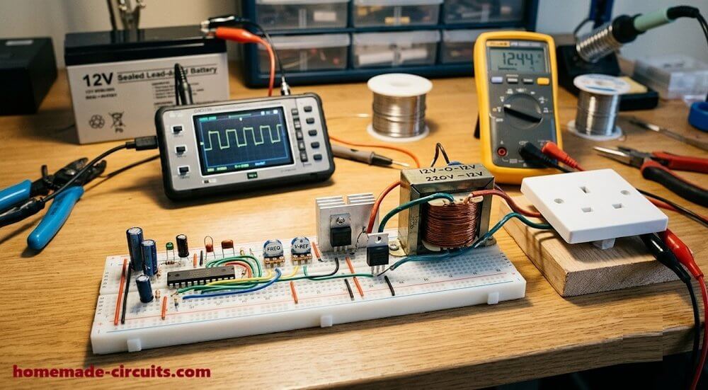
What is IC SG3525?
The SG3525 is a 16-pin PWM controller IC which is mainly used for controlling switching power supplies and inverter circuits. It has an internal oscillator, PWM comparator, error amplifier, reference voltage regulator and two alternate output driver stages.
The IC can generate two separate outputs which work alternately. This feature makes it very useful for making push-pull inverter circuits and transformer-based SMPS designs. For example in a push-pull inverter, we can use the two outputs for switching two sets of MOSFETs alternately. These MOSFETs then operate a transformer and convert the battery DC into AC.
In an SMPS circuit, the same IC can control the switching of a ferrite transformer or an inductor, so that we can get the required regulated DC output.
So the SG3525 can be used for many different types of power conversion circuits.
Main Features and Specifications of SG3525
Some important features of the SG3525 are given below.
- Operating supply voltage: 8V to 35V.
- Internal reference voltage: 5.1V.
- Two alternate PWM outputs.
- Adjustable oscillator frequency.
- Adjustable dead time.
- Internal error amplifier.
- Internal soft start facility.
- Shutdown control input.
- Undervoltage lockout.
- Separate oscillator synchronization input.
- Internal PWM latching function.
- Two source/sink output driver stages.
The oscillator frequency range and output drive specifications can slightly vary between manufacturers and different IC versions. So, you should check the datasheet of the actual IC that you are using.
SG3525 Pinout and Pin Functions
The SG3525 comes in a 16-pin DIP or surface mount package. Each pin has its own function. So, we should understand these pins properly before building any inverter or SMPS circuit.
Here is the basic pin arrangement:
| Pin No. | Pin Name | Function |
|---|---|---|
| 1 | INV Input | Inverting input of the error amplifier. |
| 2 | Non-INV Input | Non-inverting input of the error amplifier. |
| 3 | Sync | Used to synchronize the oscillator with an external signal. |
| 4 | OSC Output | Provides the oscillator waveform output. |
| 5 | CT | Timing capacitor connection for setting oscillator frequency. |
| 6 | RT | Timing resistor connection for setting oscillator frequency. |
| 7 | Discharge | Provides the discharge path for the timing capacitor. |
| 8 | Soft Start | Connected to a capacitor to provide a gradual PWM startup. |
| 9 | Compensation | Used for connecting the compensation network of the error amplifier. |
| 10 | Shutdown | Used to stop the PWM outputs when a shutdown signal is applied. |
| 11 | Output A | PWM output A for driving an external power stage. |
| 12 | Ground | Common ground connection for the IC. |
| 13 | VC | Supply voltage for the output stage. |
| 14 | Output B | PWM output B for driving an external power stage. |
| 15 | VI | Main supply voltage input for the IC. |
| 16 | VREF | Provides a regulated 5.1V reference output. |
Note: Pins 11 and 14 provide alternate PWM outputs, which are commonly used for driving push-pull and half-bridge inverter circuits.
One important thing to understand here is that pin 13 and pin 15 are not the same supply connections. Pin 15 supplies the main IC circuitry, while pin 13 supplies the output driver stages.
For more detailed information about the pin functions, internal circuit details and compensation network, you can read the following article:
Understanding SG3525 IC Pinouts:
https://www.homemade-circuits.com/understanding-sg3525-ic-pin-outs/
How SG3525 Works
The working of the SG3525 is quite simple when we understand its internal sections.
First, the oscillator section generates a fixed frequency signal with the help of the external timing resistor and capacitor connected to pins 5 and 6.
This oscillator signal is then processed by the internal flip-flop and PWM comparator sections.
The internal flip-flop activates output A and output B alternately. Because of this, the two outputs produce alternate switching pulses.
The PWM comparator controls the width of these pulses according to the control voltage received from the error amplifier.
This means we can change the ON time of the output pulses without changing the basic switching frequency.
When the PWM pulse width increases, the power transferred through the external switching stage generally increases. But when the PWM pulse width decreases, the power transfer is reduced.
The error amplifier can be used for automatically adjusting the PWM according to the output voltage or another feedback signal.
The IC also has a soft start facility. This helps the PWM output to increase slowly during startup, instead of suddenly applying maximum pulse width.
Understanding the SG3525 PWM Outputs
The SG3525 has two separate outputs at pins 11 and 14. These outputs work alternately. This means when output A is active, output B remains inactive, and after this output B becomes active.
This arrangement is very useful for push-pull inverter circuits.
For example suppose we connect two MOSFET banks to the two outputs through suitable gate driver circuits. The first MOSFET bank switches during one half-cycle, while the second MOSFET bank switches during the next half-cycle. This allows the transformer primary winding to receive alternate switching pulses.
One important thing we should understand is that the oscillator frequency and the individual output pulse repetition frequency are not always the same. In the normal alternate push-pull arrangement, each output operates at approximately half the oscillator frequency.
The maximum duty cycle of each output is also restricted. This helps to provide the required non-overlapping switching interval.
But the actual dead time must be selected according to the switching devices, driver circuit and transformer requirements.
How to Set the SG3525 Oscillator Frequency
The oscillator frequency is mainly controlled by the external resistor and capacitor connected to pins 5, 6 and 7.
Pin 5 is connected to the timing capacitor, while pin 6 is connected to the timing resistor.
Pin 7 provides the discharge path and also helps to determine the oscillator dead time.
A commonly used approximate frequency relationship is:
f = 1 / [CT (0.7RT + 3RD)]
Here:
- f = Oscillator frequency in Hz.
- CT = Timing capacitor in Farads.
- RT = Timing resistor in Ohms.
- RD = Discharge resistor in Ohms.
This is an approximate design relationship. For accurate frequency selection, we should check the values using the particular manufacturer's datasheet. The frequency should be selected according to the transformer, MOSFETs, switching losses and the intended application.
For example a low-frequency inverter and a high-frequency ferrite transformer SMPS will need completely different oscillator settings.
Important Design Considerations When Using SG3525
Although the SG3525 is a useful controller, still we should take care of a few things when using it in practical power circuits.
MOSFET gate driving
The two internal outputs can drive moderate gate loads, but when we are using high-power MOSFET banks or IGBTs, suitable external gate driver circuits may be required. This helps to provide enough gate charging current and proper switching performance.
Dead time adjustment
Dead time is very important in push-pull and bridge circuits. If the switching devices conduct at the same time in the same bridge leg, it can create a dangerous shoot-through condition.
So we must provide sufficient dead time according to the power stage and driver specifications.
Proper feedback control
The internal error amplifier can be used for regulating the output voltage. But when we need both adjustable voltage and current regulation, a properly designed external feedback circuit may be more suitable.
Soft start
The capacitor connected to pin 8 controls the soft start action. This helps to reduce sudden switching stress during startup.
Power supply decoupling
The main supply and output driver supply should have suitable local bypass capacitors. The PCB layout should also keep the high-current switching paths away from sensitive feedback and oscillator connections.
Different SG3525 Inverter and SMPS Circuit Applications
Now let us look at some practical circuits which we can build using the SG3525. I have arranged these designs according to their applications, so you can easily select the circuit which matches your requirement.
SG3525 Basic Inverter with Low Battery Cutoff and Automatic Voltage Regulation
This is a useful application of the SG3525 for making battery-operated inverter circuits. The circuit uses the alternate PWM outputs of the IC for driving the inverter MOSFETs.
It also includes additional control circuits for detecting low battery voltage and regulating the inverter output voltage.
The low battery cutoff feature helps to prevent excessive battery discharge, while the output feedback arrangement helps to maintain the required AC voltage when the load or battery condition changes. This type of design can be useful when we need a basic inverter with some additional protection and voltage correction features.
Read the complete circuit:
SG3525 Pure Sine Wave Inverter Circuit
We can also use the SG3525 for making sine wave inverter circuits with additional SPWM processing stages.
Here the basic alternate switching signals from the SG3525 are processed through external PWM circuits to obtain the required sine pulse width modulation. The resulting pulses are then used for controlling the MOSFET switching stage.
This arrangement helps to produce a much smoother AC waveform compared to a basic square wave inverter. This type of circuit can be useful when we want to experiment with SPWM generation and sine wave inverter construction.
Read the complete circuit:
SG3525 Full Bridge Inverter Circuit
A full bridge or H-bridge inverter uses four power switching devices arranged in a bridge configuration.
The SG3525 provides the required alternate PWM signals, while additional driver arrangements are used for operating the high-side and low-side MOSFETs.
The main advantage of a full bridge arrangement is that it can drive a transformer or load using both polarities of the DC supply without requiring a center-tapped primary winding. But we must properly handle the high-side gate driving and shoot-through protection. This design can be useful for builders who want to experiment with higher-power H-bridge inverter arrangements.
Read the complete circuit:
SG3525 Inverter with Adjustable Current and Voltage Feedback
In some high-power inverter and SMPS applications, controlling only the output voltage may not be enough. We may also need an adjustable current limiting facility. The internal error amplifier of the SG3525 can handle normal voltage feedback applications. But when we need independent constant voltage and constant current control, a separate external feedback arrangement can be more useful.
In this design, an external LM324 op-amp circuit processes the voltage and current feedback signals and provides a common control signal to the SG3525.
This type of arrangement can be useful for adjustable power supplies, high-power inverters and other applications where both voltage and current regulation are required.
Read the complete circuit:
SG3525 Adjustable SMPS Power Supply with CV and CC Control
The SG3525 can also be used for making an adjustable high-current SMPS power supply.
This particular design is intended to provide an adjustable output from approximately 3V to 14V, with an adjustable current range of around 1A to 10A. The design uses a forward converter power stage, an external gate driving arrangement and an LM324-based feedback section.
It also has separate constant voltage and constant current control, along with short-circuit protection. This can be a useful project for anyone who wants to make a variable bench power supply for testing electronic circuits and other low-voltage loads.
Read the complete circuit:
SG3525 SMPS Spot Welding Circuit
Another interesting application of the SG3525 is an SMPS-based spot welding machine. A spot welding machine needs very high current at a relatively low voltage but only for a short time.
In this design, the SG3525 generates high-frequency switching pulses which are used for operating the power transformer through an external bridge driver and switching stage. An additional timing circuit controls the welding pulse duration.
The transformer secondary then provides the low-voltage, high-current output required for spot welding. This type of circuit can be useful for studying high-frequency transformer switching and high-current SMPS applications.
Read the complete circuit:
Related PWM Controller: SG3524 Buck and Boost Converter Circuits
The SG3524 is another PWM controller belonging to the same general family of switching power supply controllers. We can use it for making buck converters, boost converters and other DC to DC power supply designs.
Although the SG3524 and SG3525 have closely related functions, their internal arrangements and pin functions are not exactly the same. So we should not assume that both ICs have identical pin connections or circuit arrangements.
I have included the SG3524 circuits here as related PWM controller projects, not as direct SG3525 applications. If you are interested in DC to DC converter designs, you can also check the following article.
Read the complete article:
Comparison of Different SG3525 Circuit Applications
The following table will help us understand which type of SG3525 design may be suitable for different requirements.
| Circuit type | Main purpose | Important feature | Suitable application |
|---|---|---|---|
| Basic inverter | DC to AC conversion | Battery cutoff and voltage regulation | Home inverter experiments |
| Pure sine wave inverter | DC to sine-like AC | SPWM processing | Sine wave inverter projects |
| Full bridge inverter | Bridge-based DC to AC conversion | Four-switch power stage | Higher-power inverter designs |
| Adjustable feedback inverter | Output control | Voltage and current feedback | Adjustable power conversion |
| Variable SMPS | DC to regulated DC | CV, CC and short circuit protection | Bench power supply |
| Spot welding SMPS | Low-voltage high-current conversion | Timed high-current pulses | Battery tab and metal spot welding |
How to Choose the Right SG3525 Circuit
Now let us see which circuit may be suitable for different requirements.
If you just want to build a basic battery inverter, then the inverter with low battery cutoff and automatic voltage regulation may be a good starting point.
If you want a better AC waveform then you can study the SG3525 pure sine wave inverter design using external SPWM processing.
If your requirement is a full bridge switching arrangement then the SG3525 full bridge inverter circuit will be more suitable to study.
For a variable laboratory power supply with adjustable voltage and current, you can look at the external CV/CC feedback designs.
And if you want to experiment with very high current and low voltage output, then the SG3525 spot welding SMPS design may be useful. So the correct design mainly depends on the required output voltage, current, switching frequency, transformer arrangement and protection features.
Common Design Mistakes When Using SG3525
Some common mistakes can create problems when we build SG3525 inverter and SMPS circuits.
- Using an incorrect oscillator frequency for the transformer.
- Ignoring the required dead time between switching pulses.
- Driving too many MOSFET gates directly from the IC outputs.
- Connecting the output driver supply incorrectly.
- Leaving the shutdown input improperly connected.
- Using an unsuitable feedback network.
- Ignoring transformer saturation and switching losses.
- Making long PCB connections around the oscillator and feedback sections.
- Not providing proper short-circuit and overcurrent protection.
We should also remember that the SG3525 is only a PWM controller. The actual power handling capacity of the complete circuit depends on the MOSFETs, IGBTs, transformer, gate drivers, PCB tracks and cooling arrangements.
Frequently Asked Questions
What is the main function of IC SG3525?
The main function of the SG3525 is to generate controlled PWM switching pulses for operating power switching devices in inverter and SMPS circuits.
Can SG3525 be used for making an inverter?
Yes, we can use the SG3525 for making push-pull inverters, modified sine wave inverters and inverter designs using additional SPWM processing stages.
Can SG3525 generate two alternate PWM outputs?
Yes, it has two alternate outputs at pins 11 and 14. These outputs are useful for driving push-pull switching arrangements.
What is the supply voltage required for SG3525?
The recommended operating supply range of the SG3525A is generally 8V to 35V. We should always check the datasheet of the particular manufacturer.
What is the reference voltage of SG3525?
The IC has an internal regulated reference voltage of approximately 5.1V available at pin 16.
Can SG3525 control the output voltage of an SMPS?
Yes, its internal error amplifier and PWM comparator can be used for controlling the duty cycle according to the output feedback voltage.
Can we use SG3525 for constant current power supplies?
Yes, but for accurate independent constant voltage and constant current operation, an external feedback arrangement may be required depending on the design.
What is the function of pin 8 in SG3525?
Pin 8 is the soft start pin. An external capacitor connected to this pin controls the gradual buildup of PWM output during startup.
What is the function of pin 10 in SG3525?
Pin 10 is the shutdown input. Applying an appropriate high signal to this pin disables the PWM outputs.
Is SG3525 suitable for high-frequency SMPS circuits?
Yes we can use the SG3525 for high-frequency switching power supplies. But the practical switching frequency must be selected according to the transformer, switching devices and other circuit requirements.
Conclusion
The SG3525 is a very useful PWM controller for making different types of power electronics circuits. We can use it for inverter designs, full bridge converters, adjustable SMPS power supplies, battery protection circuits and even high-current spot welding applications.
Its internal oscillator, alternate PWM outputs, error amplifier, soft start and shutdown functions make it suitable for many different switching power supply designs. The important thing is that we should select the correct power stage and feedback arrangement according to the required output specifications.
You can now explore the individual circuit designs discussed above and understand how we can use the SG3525 for different practical applications.

Need Help? Please Leave a Comment! We value your input—Kindly keep it relevant to the above topic!