If you have ever tried building a high-power inverter, a high-frequency induction heater, or just a solid adjustable lab bench power supply, you already know that controlling both the voltage and current at the same time is an absolute nightmare.
Most builders just grab the standard application circuit from the SG3525 datasheet, wire up a couple of pots to the internal error amplifier and then hope for the best. Let me tell you from bench experience: that internal error amp is completely useless if you want a true, dual-loop Constant Voltage and Constant Current variable bench supply.
The moment you hook your voltage and current adjustment pots to that same internal pin, the two loops start fighting each other. You get massive voltage sagging under load, annoying screeching noises from your transformer and a circuit that hunts or oscillates wildly.
Because this is such a major headache, so I spent a lot of time on my bench designing a bulletproof, external analog management circuit that solves everything. It uses just one cheap, common LM324 quad op-amp chip. It completely isolates your voltage and current tracking loops, wipes out diode temperature drift, handles high-speed short-circuit protection natively, and feeds a single clean control signal to the SG3525.
Remember we Used Forward Topology here, and not a Flyback...Why??
OK...let us look at the forward topology instead of flyback in a very simple way so that you can understand the difference. In a flyback topology the transformer does not work like a normal transformer. It actually works like a massive energy storing coil.
When the primary side switches turn on then the energy is stored inside the magnetic field of the core. Because of this storage we must use a big air gap in the core so that it does not saturate. When the switches turn off then that stored energy is suddenly dumped into the secondary output. This mechanism creates very high peak current stress on the MOSFETs and it makes the system inefficient for a one hundred and forty watt continuous power demand.
Now since we know that let us look at our forward topology. In a forward converter the transformer works as a true pure transformer because it transfers energy instantly.
When the primary H bridge switches are turned on then the energy goes straight from the primary side to the secondary side at the exact same microsecond. Since the energy transfer is direct so the transformer does not store energy.
Because of that we can use a highly efficient solid manganese zinc ferrite core with an absolute 0 mm air gap. This keeps our magnetizing inductance maximum and makes our core size compact. Since the current stresses on your switches are radically reduced so your output voltage tracking is fundamentally stiffer.
Then the high frequency ripple is cleanly flattened by our dedicated yellow and white iron powder output inductor L. So this makes the forward topology the ultimate choice for a robust noise isolated lab bench power supply that will not cook your components under full load.
Fine...Now let us break down exactly how the whole system works block by block, along with the precis transformer winding details so you can build this on your own bench!
Audio/Video Representation
FIRST PART: SYSTEM ARCHITECTURE AND OSCILLATOR SETUP
The main brain handling our pulse-width modulation is the SG3525 controller chip. We are running it as a fixed-frequency driver to feed a heavy-duty full H-bridge power stage.
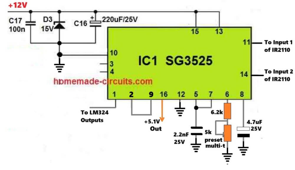
To get the absolute best efficiency out of our ferrite core without overheating our primary switching MOSFETs, we want our actual transformer switching frequency to sit right at 50 kHz. The internal oscillator of the SG3525 is controlled by the timing resistor on Pin 6, the timing capacitor on Pin 5, and the discharge resistor on Pin 7.
Because the chip toggles its dual output pins alternately every single cycle, the frequency seen by the main transformer primary winding is exactly half of the internal oscillator speed. Therefore, we target an internal clock speed of 100 kHz.
To set this up cleanly, we select a standard 2.2 nF ceramic capacitor for Pin 5 and skip the dead-time resistor completely by grounding Pin 7 directly. This leaves us needing a timing resistance of roughly 6.5 kOhm on Pin 6. Since you cannot buy that exact value off the shelf, so use a standard 6.2 kOhm fixed resistor in series with a 5 kOhm multi-turn trim-pot. This allows you to calibrate the clock precisely on your oscilloscope.
Now about bypassing that internal error amplifier....this is where most people go wrong. To let our external precision LM324 control loops govern the system without interference, we completely disable the internal amplifier inside the SG3525. All you have to do is take a small piece of jumper wire and solder it directly from Pin 2 to Pin 9. This fixes the internal amp into a passive unity-gain follower. We then feed our master external tracking signal straight into Pin 1.
Additionally because our new high-speed protection system cuts power directly at the gate drivers, then you must tie Pin 10 of the SG3525 straight to your clean analog ground plane to prevent stray electromagnetic noise from causing ghost shutdowns.
SECOND PART: THE GATE DRIVER AND FULL H-BRIDGE TOPOLOGY
For our high-power execution stage, we are using four N-channel power MOSFETs wired in a standard Full H-Bridge configuration. This topology is excellent because it allows the primary winding of our transformer to see the full potential of our rectified DC bus...which sits around +310V to +325V DC when running off standard filtered AC mains.
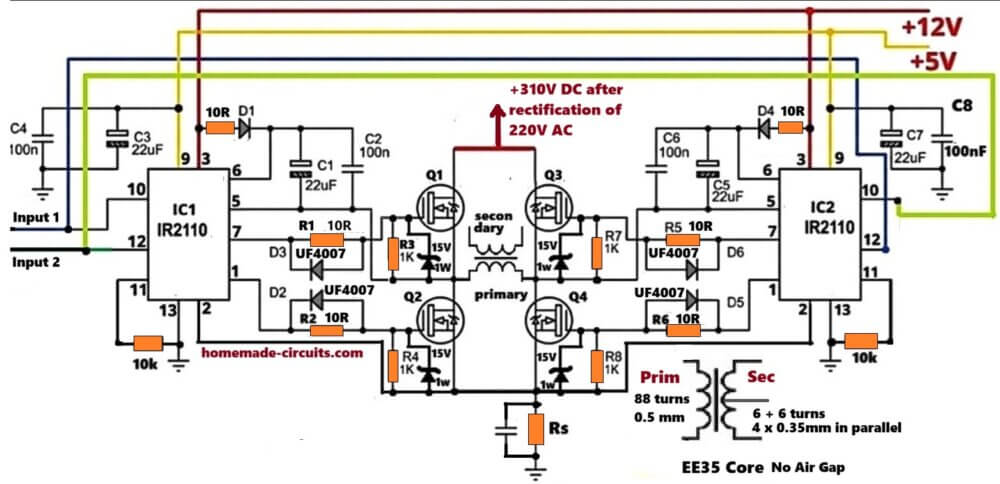
Driving the two high-side MOSFETs is a bit tricky because their gates need a floating voltage source that can swing significantly higher than the main DC power rail. To handle this effortlessly, we use two IR2110 high and low-side gate driver ICs.
For the high-side floating bootstrap supplies, we connect a fast-recovery 1N4007 or UF4007 diode from our +12V auxiliary housekeeping rail to Pin 7, paired with a 22 uF electrolytic capacitor in parallel with a 100nF ceramic capacitor placed directly between Pin 7 and Pin 5.
When the low-side MOSFET fires, Pin 5 is pulled hard to ground, then allowing the auxiliary rail to charge the bootstrap capacitors. When the high-side switch activates, then capacitor floats up and provides the necessary gate-to-source voltage to fully saturate the upper MOSFET channel.
To completely prevent high-frequency gate ringing and parasitic oscillations caused by layout trace inductance, make sure to add a 150 Ohm resistor directly in series with the gate pin of every single MOSFET. We also place a 1N4007 diode in parallel with each gate resistor to ensure an ultra-fast turn-off path, dumping the gate charge back into the driver instantly.
THIRD PART: THE PRECISION LM324 CV/CC ERROR MANAGER
To manage our smooth, continuous adjustments for both voltage and current, we utilize all four independent operational amplifiers inside a single LM324 quad op-amp package.
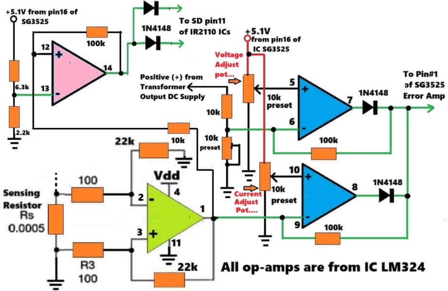
First up is the Shunt Instrumentation Amplifier. We measure the real-time return current on the low-side ground rail using a tiny 0.0005 Ohm sensing resistor. When running a full 10A load, the raw voltage drop across this shunt is incredibly small.....just 5 mV. To amplify this cleanly, the first stage of the LM324 is wired as a differential amplifier using a pair of 100 Ohm input resistors and matching 22 kOhm feedback resistors to ground. This gives us a precise differential gain of 220. At a full 10A load, Pin 1 outputs exactly 1.1V.
Next are our Constant Voltage and Constant Current tracking loops. They act as error amplifiers driving a shared, "highest voltage wins" diode OR network connected straight to Pin 1 of the SG3525.
- The Current Error Loop: Pin 10 connects to your front-panel 10k current preset pot, scaled with a padding resistor so its maximum voltage tops out at 1.1V. Pin 9 reads the live telemetry from our shunt amp. If your load tries to cross your preset threshold, Output Pin 8 swings high, then driving a 1N4148 diode to pinch the PWM duty cycle via Pin 1 of the SG3525.
- The Voltage Error Loop: Pin 5 connects to your front-panel 10k voltage adjust pot, sweeping from 0V to 5.1V using the stable reference rail from Pin 16 of the SG3525. Pin 6 samples the final output voltage rail through a divider network consisting of a 10 k,Ohm fixed resistor and a 10 kOhm multi-turn calibration trim-pot, Output Pin 7 drives a second 1N4148 diode to manage the master control line.
To completely eliminate the annoying 0.6V forward voltage drop variation of these 1N4148 diodes when your enclosure gets warm, we route a 100 kOhm feedback resistor from the shared cathodes back to the respective inverting input pins of each loop. This forms an "Ideal Diode" tracking loop that automatically auto-compensates for thermal drift... keeping your output values perfectly rock-solid regardless of temperature changes!
FOURTH PART: EMERGENCY SHORT-CIRCUIT OP-AMP SELF-LATCH
While our standard current loop handles slow, continuous overcurrent states by narrowing the duty cycle, a dead short-circuit on your workbench requires instant, hardware-level intervention to prevent your primary MOSFETs from blowing up. Instead of adding extra ICs or searching for finicky hardware SCR components, we use the 4th internal op-amp stage of our LM324 to build a high-speed electronic latch.
Here is how the latching mechanism operates: We set a fixed reference voltage of 1.32V on Inverting Input Pin 13 using a small two-resistor voltage divider running off our stable 5.1V reference. This 1.32V threshold represents our absolute emergency hazard limit of 12A. Non-Inverting Input Pin 12 continuously monitors our live shunt telemetry through a 10 kOhm resistor.
To create the lock-in action, we place a high-value 100 k Ohm positive feedback resistor directly from Output Pin 14 back to Non-Inverting Pin 12.
During normal running conditions, the telemetry voltage stays well below 1.32V, keeping our latch output on Pin 14 dead low at 0V. But the exact microsecond a short-circuit occurs and the shunt amp signal spikes past 1.32V, Pin 14 violently goes up to its positive rail at +10.5V. This high voltage travels back through our 100 kOhm feedback loop and clamps Pin 12 permanently high.
Even when the short-circuit is cleared and the shunt telemetry drops back to zero, the op-amp stays completely blinded by its own output, locking the system off safely.
To execute an immediate power cutoff, Output Pin 14 branches out into the anodes of two separate 1N4148 isolation diodes. The cathode of the first diode connects straight to Pin 11 (SD) of our left IR2110 driver, and the second connects to Pin 11 (SD) of our right IR2110 driver. This slams the gate drives down to 0V in less than two microseconds, completely isolating the power stage!
To reset the latch after clearing a fault, you can either power-cycle the unit or click a small, normally-open tactile push button wired from Pin 12 to ground to momentarily short the latch node.
FIFTH PART: MASTER TRANSFORMER AND LC FILTER SPECS
To tie everything together, here are the exact structural end results for your high-frequency magnetics and output filtering layout:
- Primary Winding:Solder a single, clean strand of 24 AWG (0.51 mm diameter) or 25 AWG (0.45 mm diameter) super-enamelled copper magnet wire for exactly 88 turns.
- Secondary Winding:Wind 6 turns plus 6 turns with a center-tap configuration. To easily carry 10A without suffering from high-frequency skin-depth power losses, bundle 4 parallel strands of 22 AWG (0.64 mm diameter) wire side-by-side like a flat ribbon and wind them simultaneously.
- Transformer Core Type:Use a standard EE35 or ETD39 ferrite core made of high-frequency PC40 manganese-zinc material. Assemble the core halves with an absolute 0 mm air gap (completely solid core with no gap).
- Output Inductor (L):Wrap 26 turns of 3 parallel strands of 20 AWG (0.81 mm diameter) magnet wire around a T106-26 iron powder toroid core (the classic yellow and white ring). Dimensions are 26.9 mm outer diameter, 14.5 mm inner diameter, and 11.1 mm height.
- Output Capacitor (C):Install a minimum of 2200 microfarads total capacity by placing two low-ESR high-frequency electrolytic capacitors of 1000 microfarads or 1200 microfarads in parallel, rated safely for 25V or 35V.
- High-Frequency Bypass:Solder a small 0.1 microfarad ceramic capacitor directly across the final positive and negative output terminal blocks to sponge up any remaining high-frequency switching ripple right at the source.
SIXTH PART: CRITICAL PCB LAYOUT RULES
When routing a high-gain analog tracking board right next to a noisy 50 kHz switching stage handling hundreds of volts, layout discipline is non-negotiable:
- Kelvin Current Sensing: Route two independent, thin signal traces directly from the pads of your 0.0005 Ohm shunt resistor all the way back to the input resistors of the LM324 shunt amp stage. Do not let these measurement tracks share copper with the heavy, pulsing ground return lines of the H-bridge.
- Star Ground Topology: Separate your noisy power ground plane from the quiet analog control ground plane. Tie these two planes together at only one single point...preferably right at the quiet ground pad of your current shunt resistor.
- Isolate the Driver Shutdown Pins: Never link Pin 11 of your two IR2110 chips directly together on a single copper trace without isolation! Tying them directly builds a high-frequency noise bridge that allows switching spikes from one side of your H-bridge to corrupt the logic gates of the opposite side, causing severe duty-cycle dropouts and blown MOSFETs. Always use those two separate 1N4148 isolation diodes!
- Local Decoupling Bypasses: Solder a 100 nF ceramic capacitor as physically close as possible between the VCC and GND pins of both the LM324 and the SG3525 to protect their logic from high-frequency EMI.
And there you have it guys! A highly sophisticated, heavy-duty adjustable bench supply utilizing smart analog routing to cram your entire control network into just one SG3525 chip, two IR2110 drivers and a single LM324 quad op-amp.
Drop a comment below if you are planning to build this or need help with your layout tracking, and happy building!


Need Help? Please Leave a Comment! We value your input—Kindly keep it relevant to the above topic!