In this post I have explained how an effective and efficient, yet very cheap, and stabilized bench power supply can be designed by any electronic hobbyist for safely testing all types electronic projects and prototypes.
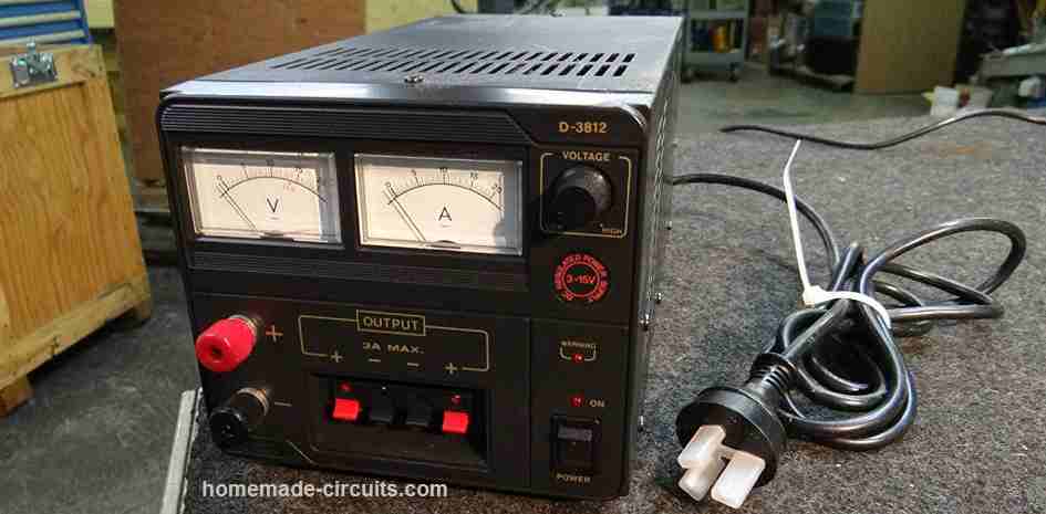
The main features that a bench power supply must have are:
- Should be built with cheap and easily available components
- Should be flexible with its voltage and current ranges, or simply must include the facility of a variable voltage and variable current outputs.
- Should be over-current and over-load protected.
- Should be easily reparable, in case a problem arises.
- Should be reasonably efficient with its power output.
- Should facilitate easily customization as per a desired specification.
Audio/Video Representation
General Description
The majority of the power supply designs thus far incorporate a linear series stabilizer. This bench power supply design uses a pass transistor which works like a variable resistor, regulated by a Zener diode.
The series power supply system is the more popular, possibly due to the fact that it is a lot more efficient. Except of some minor loss in the Zener and feed resistor, noticeable loss only happens in the series pass transistor during the period it is supplying current to the load.
However, one disadvantage of the series power supply system is that these do not provide any kind of output load short-circuit.
Meaning, during output fault conditions the pass transistor may allow a large current to flow through it, eventually destroying itself and possibly the connected load also.
That said, adding a short circuit protection to a series pass bench power supply can be quickly implemented through another transistors configured as a current controller stage.
The variable voltage controller is achieved through a simple transistor, potentiometer feedback.
The above two additions enables a series pass power supply to be highly versatile, rugged, cheap, universal, and virtually indestructible.
In the following paragraphs we will briefly learn the designing of the various stages involved in a standard stabilized bench power supply.
Easiest Transistor Voltage Regulator
A quick way of getting an adjustable output voltage is to hook up the base of the pass transistor with a potentiometer and Zener diode as shown in the figure below.
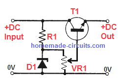
In this circuit the T1 is rigged as an emitter-follower BJT, where its base voltage VB decides its emitter side voltage VE. Both VE and VB will precisely correspond with each other, and will be almost equal, deducting its forward drop.
The forward drop voltage of any BJT is typically 0.7 V, which implies that the emitter side voltage will be:
VE = VB - 0.7
Using a Feedback Loop
Although the above design is easy to build and very cheap, this type of approach doesn't offer great regulation of power at the the lower voltage levels.
This is exactly why a feedback type control is normally employed to get an improved regulation throughout the entire voltage range, as demonstrated in the figure below.
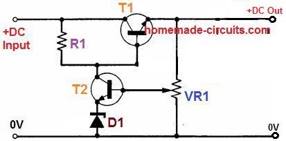
In this configuration, the base voltage of T1, and therefore output voltage, is controlled by the voltage drop across R1, mainly due to the current pulled by T2.
When the slider arm of the pot VR1 is at the ground side extreme end, T2 becomes cut off since now its base becomes grounded, allowing the only only voltage drop across R1 caused by the base current of T1.
In this situation the output voltage at the T1 emitter is going to be almost same as the collector voltage, and can be given as:
VE = Vin - 0.7, here VE is the emitter side voltage of T1, and 0.7 is the standard forward voltage drop value for BJT T1 base/emitter leads.
So if the input supply is 15 V, the output can be expected to be:
VE = 15 - 0.7 = 14.3 V
Now, when the pot VR1 slider arm is moved to the upper positive end, will cause T2 to access the whole emitter side voltage of T1, which will cause T2 to conduct very hard.
This action will directly connect the zener diode D1 with R1. Meaning, now the base voltage VB of the T1 will be simply equal to the zener voltage Vz. So the output will be:
VE = Vz - 0.7
Therefore, if the D1 value is 6 V, the output voltage can be expected to be just:
VE = 6 - 0.7 = 5.3 V, so the zener voltage decides the minimum possible output voltage that could be obtained from this series pass power supply when the pot is rotated at its lowest setting.
Although the above is easy and effective for making a bench power supply, it has a major disadvantage of not being short circuit proof.
That means, if the output terminals of the circuit is accidentally short circuited, or an over load current is applied, the T1 will quickly heat up and burn.
To avoid this situation, this circuit could be a simply upgraded by adding a current control feature as explained in the following section.
Adding Overload Short Circuit Protection
A simple inclusion of T3 and R2 enables the bench power supply circuit design to be 100% short-circuit proof and current controlled. With this design even an intentional shorting at the output will not cause any harm to the T1.
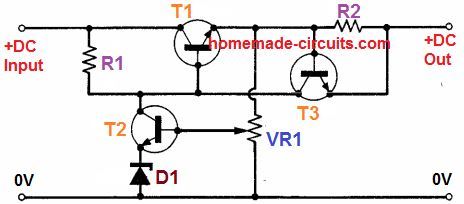
The working of this stage could be understood as follows:
As soon as the output current tends to go beyond the set safe value, a proportional amount of potential difference across R2 is developed, enough to switch ON transistor T3 hard.
With T3 switched ON causes T1 base to be joined with its emitter line, which instantly disables the T1 conduction, and this situation is maintained until the output short or overload is removed.
In this way T1 is safeguarded from any undesired output situation.
Adding a Variable Current Feature
In the above design, the current sensor resistor R2 can be a fixed value if the output is required to be a constant current output.
However, a good bench power supply is supposed to have a variable range for both voltage and current.
Considering this demand, the current limiter could be made adjustable simply by adding a variable resistor with the base of T3, as shown below:
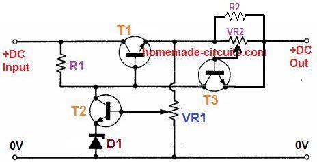
VR2 divides the voltage drop across R2 and thus allows the T3 to switch ON at a specific desired output current.
Finalized Design of a Basic Bench Power Supply Circuit
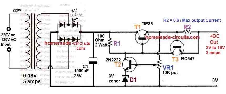
Calculating the Part Values
Let's start with the resistors, R1 can be calculated with the following formula:
R1 = (Vin - MaxVE)hFE / Output Current
Here, since MaxVE = Vin - 0.7
Therefore, we an simplify the first equation as R1 = 0.7hFE / Output Current
VR1 can be a 10 k pot for voltages up to 60 V
Current limiter R2 can be calculated as given below:
R2 = 0.7 / Max Output Current
Max output current should be selected 5 times lower than T1 maximum Id, if T1 is required to work without an heatsink. With a large heatsink installed on T1, the output current can be 3/4th of T1 Id.
VR2 can be simply a 1k pot or preset.
T1 should be selected as per the output current requirement. T1 Id rating should be 5 times more than the required output current, if it is to be operated without a heatsink.
With a large heatsink installed, the T1 Id rating should be at least 1.33 times more than the required output current.
The maximum collector/emitter or VCE for T1 should be ideally twice the value of the maximum output voltage specification.
The value of zener diode D1 can be selected depending on the lowest or the minimum voltage output requirement from the bench power supply.
The T2 rating will depend on the R1 value. Since the voltage at collector of T2 will be always equal to Vin, the VCE of T2 should be higher than the Vin or the input supply.
The Id of T2 should be such it is able to handle the base current of T1, as determined by the value of R1
The same rules apply for T3 also.
In general T2, and T3 can be any small signal general purpose transistor such as BC547 or maybe a 2N2222.
Practical CV, CC Bench Power Supply Circuit Design
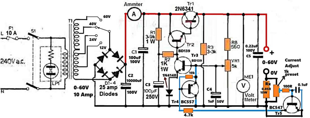
Having understood all the parameters for designing a customized bench power supply, it's time to implement the data in a practical prototype, as shown below:
How it Works
So mains comes in, 220VAC, and transformer steps it down. We have multi tap secondary, 12V, 24V, 40V, 60V, so now you can choose. If you select higher tap, then you get higher max output, but transistor suffers more heat. If you select lower tap, then dissipation drops, heat becomes less, survival improves.
This part is mainly for thermal safety, otherwise 2N6341 bjt will fry quickly.
Now rectifier stage.
D1…D4 bridge, which converts AC into pulsating DC. After bridge, DC roughly Vac into 1.414, so if 60V AC, then around 84V DC no load.
Then comes the 10,000uF capacitor which smooths 100Hz ripple, gives peak current when load suddenly pulls, and reduces regulator stress. Ripple is roughly I upon f into C. If current is high and C small, then ripple is big, simple. This capacitor decides how raw or dirty the DC is before regulation, hmm.
Next, heart of the circuit is BJT 2N6341.
This transistor runs in linear mode, not switching. It drops extra voltage. Power dissipation = (Vin − Vout) into I load. If Vin high and Vout low and current high, then heat becomes huge. Therefore big heatsink is mandatory. It behaves like variable resistor, which is controlled by BD139 stage.
Now Tr2 BD139 is like middle muscle. It amplifies control current and drives base of 2N6341. If control loop pushes more base current here, then pass transistor conducts more. If control loop pulls it down, then output reduces.
Now in this Voltage control loop now, there is NPN voltage adjust transistor. It watches output voltage through divider and preset. If output rises above set value, then this transistor reduces drive to BD139, so 2N6341 conducts less, output comes down. If output falls, then drive increases, output climbs. This is Classic negative feedback, nothing exotic.
Next comes the crucial current sensing, or the over current, over load protection, or the constant current CV feature.
Resistor Rx, let's say is 0.05Ω or 0.1Ω, having at least 10 watts. All load current flows through it. So Vsense = Iload into Rx. If Rx = 0.05Ω and current 10Amps, then 0.5V appears across it. That voltage gives the current information.
BC547 watches this.
Emitter on load side of Rx, base on supply side through 100Ω. If Vsense approaches 0.6V, then BC547 turns on. Then I_limit ≈ 0.6 upon Rx. So if Rx 0.05Ω, then limit around 12 Amps. If preset adjusts base voltage fraction, then limit shifts accordingly.
Now lets' check the BC557 role.
When BC547 turns on, then BC557 also turns on strongly. BC557 pulls down base of voltage adjust transistor. If that base gets pulled hard, then output voltage collapses quickly.
So instead of soft limiting, it clamps firmly. That gives proper CC behavior to this bench power supply circuit.
We also added 1N4148 in emitter of voltage adjust transistor.
That diode compensates Vbe, improves shut off symmetry, makes CC transition sharper, reduces leakage when limiting.
There is also small capacitor across base emitter of BC547.
If multi transistor chain exists and no cap used, then oscillation can happen. If cap is added, then CC transition smooths, high frequency hunting reduces. Stability improves.
Now how both CV, CC, modes work together, let us see.
If load is light, then current is small, voltage across Rx is small, BC547 is off, BC557 is off, voltage loop is fully in control. so Supply behaves in CV mode.
If load gets heavy or short circuit happens, then current rises, Vsense increases. If it crosses the set threshold, then BC547 becomes on, then BC557 is also turned on, causing the voltage adjust BJT Tr3 transistor base to get clamped. so Drive to 2N6341 reduces, causing output voltage to fall. Due to this
Current then stabilizes around the set limit. Here, the Supply enters CC mode.
So what does this lab power supply or the bench power supply circuit design achieve?
Its gives you True CV, true CC, low side sensing which is clean, improved clamping through PNP stage, compensation for stability, adjustable voltage and current, multi tap helps thermal handling. For fully discrete transistor lab supply, this is strong build.
However, still a few practical things remain.
Rx must handle high wattage, otherwise it burns. Heatsink must be very large, if not then transistor dies. No crowbar OVP is added yet, no thermal shutdown can be seen in this design.
Current accuracy depends on Vbe stability, which drifts with temperature, so those are the few things that needs to be improved further…
Functionally though, yes, it behaves like proper lab power supply. Not the enhanced IC type, but still a good solid discrete type of design.
Very Simple Bench Power Supply Circuit with Constant Current Output
This benchtop power supply circuit shown below is a simple and inexpensive option for hobbyists, yet is able to provide a continuously adjustable DC output with a constant current.
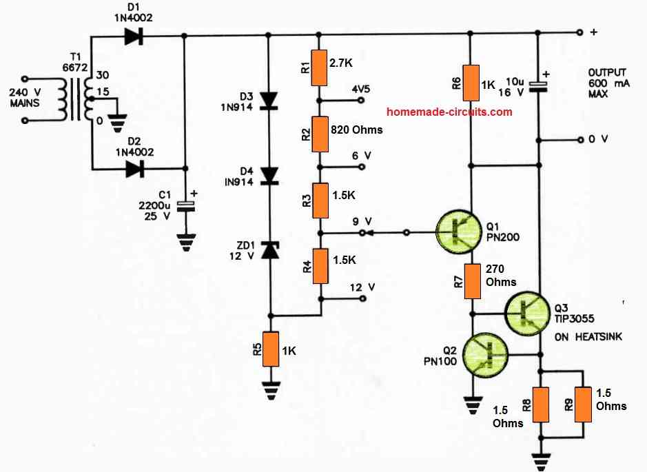
All of the components are readily available at electronics retailers. The simple 15V step down transformer is used which allows it to deliver up to one amp of output current.
A full-wave rectifier converts the AC input voltage to unregulated DC. A zener diode and two other diodes provide a regulated reference voltage for the regulator circuit.
Resistors R1 through R4 are connected to the reference voltage to produce output voltages of 4.5, 6, 9, and 12 volts. Resistor R5 provides bias current for the zener diode.
Three transistors, Q1 and Q3, form a conventional series regulator. A 10uF capacitor across the output terminals helps to reduce the AC impedance of the power supply.
Q2 along with the resistors R8 and R9 constitute the current control circuit stage which enables a constant current output.
Resistors R8 and R9 determine the output current limit, or simply the constant current value.
Op Amp Controlled Precision Bench Power Supply
The working procedure of the opamp controlled bench power supply circuit is fairly basic uncomplicated, since regulated power supplies can be simply as particular forms of feedback amplifier.
In this concept, the R1 and R2 generate a refernce sample signal from the output supply, which is by another reference voltage created by D2.
The resulting correction signal is supplied back through the 741 on the series pass transistor Q1.
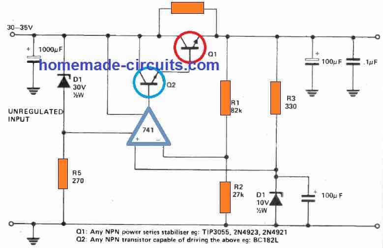
Observe that the circuit stability has been enhanced by providing the reference source R3 -D2 through the stabilized output rather than from the unstabilised input as is usually done inother bench power supplies.
To ensure that the circuit initiates as soon as switched on, a leakage resistance R4 is placed in parallel with the series pass device.
This means that the feedback loop begins to run as soon as power is switched ON.
Absolutely no regulation is sacrificed because of R4, since it is the general output which is sampled by R1 -R2, therefore, the impact of the ripple current moving through R4 gets adjusted through the feedback.
Making the Output Adjustable
The output may well be made adjustable by changing R1-R2 with a potentiometer, however in its existing layout, the circuit can't be forced to regulate under the zener voltage value of D2.
When uninterrupted adjustment of the output voltage is necessary, the reference source R3-D2 should be furnished through the unregulated input, with accompanying minor lack of stability.
The quantity of power the circuit is able to offer will be limited primarily by the current handling capacity of Q1 and the maximum power capacity of the unregulated supply.
More Elaborate Bench Power Supply Circuit
A regulated bench Power supply are normally a useful gadget for any hobbyists or engineer.
Despite the truth that IC based voltage regulators have become very easily accessible, a circuit only employing ordinary discrete components can be appealing.
In order to save power, and to restrict the dissipation across the series regulator, the entire 0-30 V control range is further divided into 3 scaled-down voltage ranges.
All the 3 ranges matches with a suitable secondary supply voltage (determined by the position of S1a) and a proper reference voltage (determined by S1b).
So that you can get a consistent control of the output voltage to a minimum of0 V, a negative auxiliary supply needs to be added.
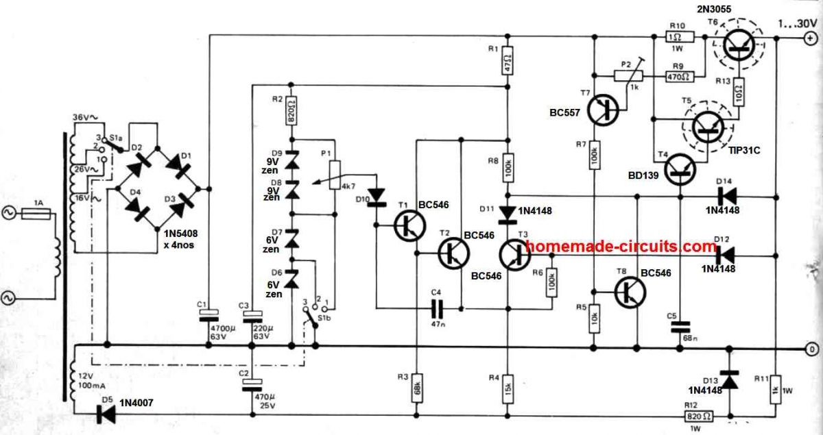
In this bench power supply circuit, this is extracted (by means of D5 and C2) via a different 12 V winding over the mains transformer. A different option could be to incorporate an additional separate mains transformer.
The final results tested on the bench prototype are pretty decent: ±35 V mains voltage swing induced just ±25 mV swing of the output voltage, with full load 1 amp load attached to the output. The A.C. ripples of the output (hum) had been lower than 15 mV.
How it Works
The circuit functions in the following manner.
A reference voltage, extracted through the zener diode(s) D6 -D9 and fixed using pot P1, is directed to the transistor T2 base by means of D10 and TI.
T2 and T3 work like a differential amplifier; wherein the base of T3 receives the output voltage by means of DI2. This differential amplifier's output is applied, through D11, on the base of the combined series regulator made up of transistors T4, T5 and T6.
Although the configuration might look a bit complex, it works like a typical regulator circuit; it maintains the output voltage virtually fixed over an extensive range of output currents.
Transistors T7 and T8 along with connected parts form the current limiter stage. As soon as the voltage over R10 gets to a particular value (as fixed by P2) T7 begins conducting.
This, consequently, causes transistor T8 to get biased and starts conducting; which reduces the base drive to transistor T4, and the situation decreases the output voltage hence the output current continues to be inside the predetermined boundary.
When S1 is selected at position 1, that compares to an output range of 0-10 V, setting at 2 allows 10-20 V and adjusting at position 3 provides an output range of 20-30 V. P1 is used for tweaking the range as fixed by S1.
The highest amount of output current can be established using pot P2. This P2 pot could be either pre-programmed to supply a highest output current of 1 A or employed like a variable output current control.


Questions & Answers
Hello
I have assembled Practical CV, CC Bench Power Supply Circuit Design.
I have a problem at voltage section which is the voltage dont come under 9v.
The input is 30v.
Hi, Please disconnect BC557 stage from base of TR3, and check whether the issue is still there or not…
Max output current in first circuit? If lower than 3A, how to increase the current to 3A?
Please adjust the current limiting resistor value accordingly…
Also, is C2 in finalized design 10000µF or 1000µF?
In the first finalized design it is 1000uF, and in the second it is 10,000uF due to difference in current.
Can I use 15V normal transformer in the second circuit? (One that has only two output wires)
Yes, you can use 15V transformer..
I do want to make another module in compact form. Similar to bench power supply but multiple fixed output.
Like I’m giving input of 20v upto 100w. Using a pd trigger. Now i want fixed voltage of 5v, 9v, 12v, 15v, and 24v. (Maybe 20v too if not much work) How can I pull it off? I want it to be compact too. Max 4 amp is ample for the use. As it will be a emergency power supply for me so I can use my wifi mobiles and even other small electronics when no electricity is there.
I will plug it in my powerbank and run the appliances
You can try the following buck converter design, and get 5V,9V,12V,15V,20V by making either R2 or R1 variable. But 24V is not possible from 20V input unless another boost converter module is hooked up:
Can the voltage of the finalized design be increased by any means
It can be increased by upgrading the transistors accordingly.
Good evening Sir,
thanks once more thus circuit is really really good. I am enjoying it
Thank you Ngang, I am glad you are enjoying the bench power supply design, all the best to you!
Mr. Swagatam, my name is ed. I sometimes see a resistor identified as say 4R immediately followed by a number say 5 shown as 4R5. what does the 5 mean?
Please respond to my email address. Thank you very much
for your effort and work in this area, regards, Ed
Hi Ed,
4R refers to 4 Ω, or 4 ohms.
And 4R5 refers to 4.5 Ω, or 4.5 Ohms.
Let me know if you have any further questions.
Ref. Practical Design.
Hi Swagatam,
I have build this Power Supply, but I am not sure if it perform correctly. I have rebuild it 3 times just to make sure that every thing is correct, but I get the same results every time. I have replaced all the transistors with new ones. I have taken some voltage measurements and they are as follows by adjusting the 5k pot to its min. & Max. Position.
Input V = 16.34DC
Output V = Max 6.9 – Min 1.73
Q1(Tip3055) B = Max 7.4 – Min 2.3
E = Max 6.8 – Min 1.74
C = 16.34
Q2(2N2222) B = Max 8.0 – Min 2.9
E = Max 7.4 – Min 2.3
C = 16.34
Q3(BC639) B = Max 1.43 – Min 0V
E = Max 8.0 – Min 2.91
C = Max 0.77
Q4(BC639) B = Max 6.8 – Min 1.74
E = Max 6.8 – Min 1.75
C = Max 8.0 – Min 1.74
I have removed R9 & replaced with a jumper to GND.
Replaced Zener diode(D5) with 1N4148.
The fact that the cct is adjusting the output voltage indicates to me that it works OK, except I thought that the output voltage should be higher?
Your advice will be much appreciated.
Regards
Jan
Hi Swagatam,
If I disconnect the base of Q3 the output is 5.55V.
If I ground the base the output is 6.8v.
Hi Jan,

In that case something may be wrong with your circuit somewhere, because when you disable the TR3 BC547 then the 2N3055 and the 2N2222 Darlington pair have no restrictions and conduct fully, which means its collector voltage will fully appear at its emitter, except the 1.2V drop.
Please check again by connecting a dummy load of 1k resistor across the output of the circuit, or parallel to your meter probes and check the response.
Alternatively, you can also try the following basic design to test your transistor response, you can remove the zener diode, it is not required:
Make sure to connect a dummy load resistor of 1k across the output of the circuit.
Good Day Sir,
Thanks very much for this circuit.
I am done constructing it. And it is varying perfectly. But I have the same issue Jan is raising. I have a max. output of dc 7.1V . When I ground the base of Tr.3 I have my full dc out of 24V.
What should I do?
Thanks
Hello NGang,
The problem faced by Mr.Jan was due to a connection fault in his design, and it was solved by him after the necessary correction was made.
However, if you are getting the full 24V on grounding the base of TR3 that means your circuit is working alright.
Please remove the R9 resistor and the D5 diode, and replace them with jumpers and check the response…
Let me know how it goes.
Thanks very much Sir.
l have done so and it’s working perfectly. can I couple it ?
Thanks Ngang. Glad to know it is solved now!
Sorry, I could not understand what to meant by “can I couple it?”
Kindly elaborate…
Hi Swagatam,
Thank you very much. Your analysis was correct. I made a PCB track error. I corrected it and the cct works 100%. I guess we learn by our mistakes, well at least I did.
Once again thank you for your assistance and a great site.
Regards
Jan
You’re most welcome, Jan!
Great to hear that the problem is solved!
Yes, indeed, we learn from our mistakes and that’s how we move towards perfection…
All the best to you!
Good morning Sir.
I was asking if I should allow the jumpers there permanently?
Good Morning Ngang, yes, definitely, you can keep the jumpers permanently connected for the specified results…
Hi Jan, please disconnect the TR3 base from the pot and manually ground the base of the TR3 by shorting its base with the ground line and check the output voltage.
This will completely turn OFF the TR3 and allow the full output voltage of 16.34 – 1.2 = 15.14 Volts. 1.2V is the internal drop across TR1/TR2.
Please check this and let me know, then we will know who is the culprit in your circuit.
Good day Sir,
Why is the Ammeter on the practical circuit above positioned immediately after rectifier instead of at the out put. So that it is in series with the load.?
Hi NGANG,
The ammeter must be always in series with the load, so yes here the ammeter is in series with the load and also the entire circuit.
It means, in this position the ammeter will not only indicate the load current but also the current consumed by the circuit itself, if any.
hello Mr Swagatam;
My batteries group are : 6 x 12V= 72V and 80 A each.
But I have only the charger with 2,5 A capacity. When I measure the current I read about 6 A
on the multimeter while charging.
This may be harmfull to the charger or no problem?
Hello Suat,
For a 80 Ah lead acid battery, the minimum recommended charging current is 8 amps, so 6 amp will not cause any harm.
I see 6 amp would be not cause any arm. Charger unit is also safe? since it is only 2,5 amp. Thanks
Yes, but a 2.5V charger should not produce 6 amp current.
that was the problem so I had written for your comment then maybe my multimeter is wrong or I used AC current side I will check again
OK no problem…
Hello Mr Swagatam I am Oklama, I have been reading through your work and testing some of your circuits I must say this is good work and thanks for putting it out here for us to see. I have built a LPS before but now I am tasked to build a SMPS, I have a multi output transformer which will be connected to the outlet, it has a maximum current output of 1A and maximum output voltage of 18V AC. my power supply is suppose to have a back up battery which should be charging when the main power supply is on. it is a 12V rechargeable lithium battery, I need at least 4 output voltages some of which have to be negative, if you do not mind sir could you please provide me with the list of components with specifications together with a possible circuitry I can get in order to accomplish this task. I would really appreciate your response if you need more information about this please let me know. Thanks a lot Sir.
Hello Oklama, I appreciate your question, and I really wish I could help you, however I am sorry, I don’t think the specific SMPS that that you have asked is available with me. Therefore I am unable to solve your requirement. Moreover a readymade transformer cannot be used for an SMPS, the transformer has to be specifically calculated and designed for an SMPS circuit.