In this article I will comprehensively discuss how to make customized transistorized voltage regulator circuits in fixed modes and also variable modes.
All linear power supply circuits which are designed to produce a stabilized, constant voltage and current output fundamentally incorporate transistor and zener diode stages for getting the required regulated outputs.
These circuit projects using discrete parts can be in the form of of permanently fixed or constant voltage, or stabilized adjustable output voltage.
What is a Voltage Regulator
The main function of a DC voltage regulator circuit is to generate a voltage and current that is fixed and constant at a certain specified levels.
Thus, a regulator is used in a power supply to keep the output voltage or current within certain fixed limits.
Simplest Voltage Regulator
Probably the simplest type of voltage regulator is the zener shunt stabilizer, which works by using a basic zener diode for the regulation, as demonstrated in Figure below.
The zener diodes have a voltage rating equivalent to the intended output voltage, that may be closely match the desired output value.
As long as the supply voltage is below the rated value of the zener voltage, it exhibits maximum resistance in the range of many megohms, allowing the supply to pass without restrictions.
However, the moment the supply voltage increases over the rated value of 'zener voltage', triggers a significant drop in its resistance, causing the over voltage to get shunted to ground through it, until the supply drops or reaches the zener voltage level.
Due to this sudden shunting the supply voltage drops and reaches the zener value, which causes the zener resistance to increases again.
The cycle then continues rapidly ensuring the supply remains stabilized at the rated zener value and is never allowed to go above this value.
To get the above stabilization, the input supply needs to be a little higher than the required stabilized output voltage.
The excess voltage above the zener value causes the internal "avalanche" characteristics of the zener to trigger, causing an instant shunting effect and dropping of the supply until it reaches the zener rating.
This action continues infinitely ensuring a fixed stabilized output voltage equivalent to the zener rating.
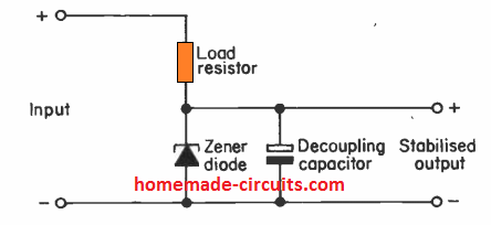
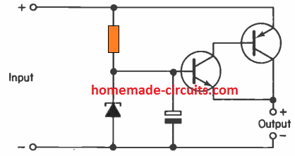
Practical Simplest Zener Regulator
The most basic regulator employs a two-terminal device such as a zener diode with the characteristic of keeping a constant voltage across it. Figure 1 below depicts the basic circuit.
Zener diodes could be connected in series in any configuration for achieving even higher voltages.
A current-limiting (ballast) resistor must be incorporated, as these devices would try to retain constant terminal voltage by pulling whatsoever current is available from the power source.
Efficiency is essential.
The regulating device's impedance might be quite low, and it could rapidly drain catastrophic quantities of current in the absence of a limiting resistor, and get damaged.
Therefore a limiting resistor becomes necessary for a zener diode. Because the regulating component is shunted across the load, this type of zener circuit (Fig. 1) is often called a shunt-type regulator.
This method works extremely well for low-power applications when just a few milliamperes of current are needed and regulation (% change of voltage or current under different loads) of just few percent is enough.
Since the entire current flowing through the limiting resistor is the sum of the load current plus the regulator current required to maintain the voltage, efficiency is often poor, particularly at low loads.
High amounts of current is able to pass through the regulator when the load is disconnected or changed. While this is not an issue for tiny circuits such as an oscillator circuit that draws only a few milliamperes, it can be an issue in a circuit like a tiny digital device that might require around 1 amp at 5 volts.
In some circumstances (LED lights, on-off switches), the system may use less than 50 milliamps in standby mode and 1 amp in active mode.
A zener-diode regulator would be highly ineffective in such cases as it will have to pass roughly 1 amp through the zener while the system were idle and therefore not consuming its operational current.
In such scenario if the input voltage was 12 volts, the efficiency of the 12V to 5V regulator might be extremely low due to the presence of a constant load of above 1 amp on the 12 volt supply, even if the load on the 5 volt supply side was small.
This equates to 12 watts or even more heat creation, which is an extremely inefficient condition.
An easy remedy is to employ an active regulator which might not demand so much current to operate.
It should be noted, however, that there will always be some voltage loss across the regulator. Because the regulator circuit is an amplifier, it will itself require some voltage to function.
The pass transistor's base-emitter voltage is 0.6 to 0.7 volts, and there will be some voltage loss in the bias resistors.
The input voltage must be consistently at least 2 to 5 volts higher than the highest anticipated output voltage; it must never go below this level or else the output control will be affected.
This minimum voltage must always be maintained under minimal-input-line-voltage situations at full load.
Below this threshold, instantaneous changes owing to input-supply ripple, load transients, and so on will result in a loss of regulation ( "drop-out ").
Advantages of Zener Voltage Stabilizer
Zener diodes are very handy where low current, constant voltage regulation is required.
Zener diodes are easy to configure and can be used to get a reasonably accurate stabilized output under all circumstances.
It only requires a single resistor for configuring a zener diode based voltage regulator stage, and can be quickly added to any circuit for the intended results.
Disadvantages of Zener Stabilized Regulators
Although a zener stabilized power supply is a quick, easy and effective method of achieving a stabilized output, it includes a few serious drawbacks.
- The output current is low, which may support high current loads at the output.
- The stabilization can happen only for low input/output differentials. Meaning the input supply cannot be too high than the required output voltage. Otherwise the load resistance may dissipate huge amount of power making the system very inefficient.
- Zener diode operation is generally associated with the generation of noise, which may critically affect the performance of sensitive circuits, such as hi-fi amplifier designs, and other similar vulnerable applications.
Using "Amplified Zener Diode"
This is an amplified zener version which makes use of a BJT for creating a variable zener with enhanced power handling capability.
Let's imagine R1 and R2 are of the same value., which would create sufficient biasing level to the BJT base, and allow the BJT to conduct optimally.
Since the minimum base emitter forward voltage requirement is 0.7V, the BJT will conduct and shunt any value that's above 0.7V or at the most 1V depending on the specific characteristics of the BJT used.
So the output will be stabilized at 1 V approximately. The power output from this "amplified variable zener" will depend on the BJT power rating and the load resistor value.
However this value can be easily changed or adjusted to some other desired level, simply by changing the R2 value. Or more simply by replacing R2 with a pot.
The range of both the R1 and R2 Pot can be anything between 1K and 47K, to get a smoothly variable output from 1V to the supply level (24V max).
For more accuracy, you can apply the following voltage divider formula:
Output Voltage = 0.65 (R1 + R2)/R2
Drawback of Zener Amplifier
Yet again, the drawback of this design is a high dissipation which increases proportionately as the input and the output difference is increased.
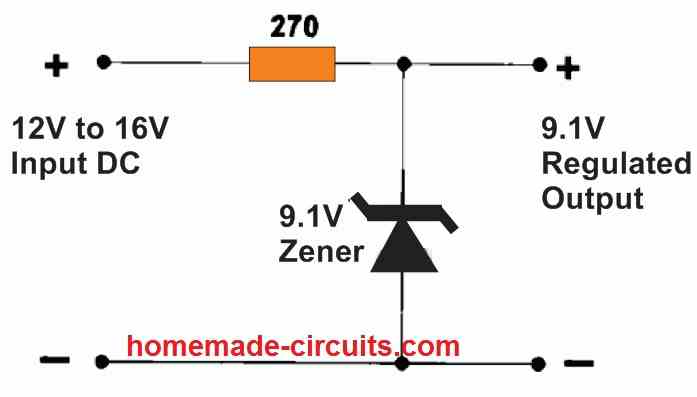
To correctly set the load resistor value depending on the output current and the input supply, the following data can be applied appropriately.
Suppose the required output voltage is 5V, the required current is 20 mA, and the supply input is 12 V. Then using Ohms law we have:
Load Resistor = (12 - 5) / 0.02 = 350 ohms
wattage = (12 - 5) x 0.02 = 0.14 watts or simply 1/4 watt will do.
Series Transistor Regulator Circuit
Essentially, a series regulator which is also called series pass transistor is a variable resistance created using a transistor attached in series with one of the supply lines and the load.
The resistance of the transistor to current automatically adjusts depending on the output load, such that the output voltage remains constant at the desired level.
In a series regulator circuit the input current has to be slightly more than the output current. This small difference is the only magnitude of current that is utilized by the regulator circuit on its own.
Advantages of Series Regulator
The primary advantage of a series regulator circuit compared to a shunt type regulator is its better efficiency.
This results in minimal dissipation of power and wastage through heat. Because of this great advantage, series transistor regulators are very popular in high power voltage regulator applications.
However, this may be avoided where the power requirement is very low, or where efficiency and heat generation are not among the critical issues.
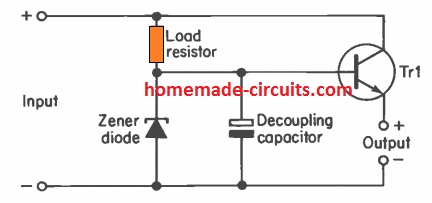
Basically a series regulator could simply incorporate a zener shunt regulator, loading an emitter follower buffer circuit, as indicated above.
You may find unity voltage gain whenever an emitter follower stage is employed. This means when a stabilized input is applied to its base, we will generally achieve a stabilized output from the emitter as well.
Because we are able to get a higher current gain from the emitter follower, the output current can be expected to be a lot higher in comparison to the applied base current.
Therefore, even while the base current is around 1 or 2 mA in the zener shunt stage, which also becomes the quiescent current consumption of the design, the output current of 100 mA could be made available at the output.
The input current is add up to the output current together with 1 or 2 mA utilized by the zener stabilizer, and for that reason the efficiency achieved reaches to an outstanding level.
Given that, the input supply to the circuit is sufficiently rated to achieve the expected output voltage, the output may be practically independent of the input supply level, since this is directly regulated by the base potential of Tr1.
The zener diode and decoupling capacitor develop a perfectly clean voltage at the base of the transistor, which is replicated at the output generating a virtually noise free volatge.
This allows this type of circuits with the ability to deliver outputs with surprisingly low ripple and noise without including huge smoothing capacitors, and with a range of current that may be as high as 1 amp or even more.
As far as the output voltage level is concerned, this may not be exactly equal to the connected zener voltage.
This is because there exists a voltage drop of approximately 0.65 volts between the base and emitter leads of the transistor.
This drop consequently needs to be deducted from the zener voltage value to be able to achieve the minimal output voltage of the circuit.
Meaning if the zener value is 12.7V, then the output at the emitter of the transistor could be around 12 V, or conversely, if the desired output voltage is 12 V, then the zener volatge must be seleced to be 12.7 V.
The regulation of this series regulator circuit will never be identical to the regulation of the zener circuit, because the emitter follower simply cannot possess zero output impedance.
And the voltage drop through the stage has to rise marginally in response to increasing output current.
On the other hand, good regulation could be expected when the zener current multiplied by the current gain of the transistor reaches minimum 100 times the expected highest output current.
A Practical Voltage Regulator Project using Transistor Emitter Follower
In the following practical voltage regulator project, an emitter follower transistor is employed to minimize the current used by the regulator device.
The zener diode is receiving 10 or 20 mA. This voltage is applied to the base of the transistor, which is referred to as the "pass" transistor since it is positioned to pass the load current.
This could be a high-power transistor rated to handle many amps of current.
The load current is made up of the collector current, which makes up the bulk of the current, and the base current.
The base current is equal to the collector current divided by the transistor's DC gain (or beta, which is normally equal to 50).
Assuming the transistor has a current gain β of 50 and a load current of 1 amp, the collector current can be calculated as given below
Collector current = β/(β+1) = 1 amp or 50/51 amps.
Base current can be calculated using the following formula:
Base Current = 1 /(β +1) or 1/51 amp.
This is somewhat less than 20 milliamperes. Figure 2 above depicts the basic regulator design.
High Current Series Regulator using Darlington Transistors
To precisely achieve this this often implies that a few transistors, may be 2 or 3 should be used so that we are able to attain satisfactory gain at the output.
A fundamental two transistor circuit project applying an emitter follower Darlington pair is indicated in the following figures exhibits the technique of applying 3 BJTs in a Darlington, emitter follower configuration.
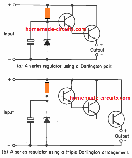
Observe that, by incorporating a pair of transistors results in a higher voltage drop at the output of approximately 1.3 volts, through the base of the 1st transistor to the output.
This is due to the fact that roughly 0.65 volts is shaved off from across each of the transistors.
If a three transistor circuit is considered, this could mean a voltage drop of slightly below 2 volts across base of the 1st transistor and the output, and so on.
Practical Circuit Using a Darlington with Pass Transistor
The following voltage regulator circuit project illustrates how an auxiliary transistor could be used as an intermediate stage if the pass transistor happens to be a very high current, low hFE device.
The intermediate transistor is configured as a Darlington pair with the pass transistor significantly increase its current gain and also enhance its current transfer ability.
It should be noted that when there is no load, the only current consumed by the circuit is that of the zener diode only.
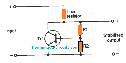
Creating an Adjustable Regulator
It is also possible to attach a variable resistor or a pot across the zener diode and if you connect the wiper of the pot to the base of the transistor, you can achieve a variable output voltage as depicted in Fig. 4 below.
The issue with this circuit is that it is no better (in fact, somewhat worse) than a zener diode as a regulator. There is no system in place to ensure that the output voltage to the load remains constant.
Furthermore, the base-emitter drop in the pass transistor causes a tiny reduction in output voltage (0.6 to 0.7 volts per transistor typically).
If the potentiometer is being used to change the output voltage, you may find an extra loss due to the pot resistance.
This resistance results in a decrease in regulation. The regulator has no way of knowing if the output voltage has dropped.
What's truly needed is a means to sense the output voltage, compare it to a set reference, and change the output voltage to the appropriate value automatically.
This necessitates the use of a feedback mechanism to regulate the output voltage. With a few more elements, we'll show you a really simple approach to achieve this.
Common Emitter Voltage Regulator with Negative Feedback
A nice configuration is at times seen in specific linear voltage regulator projects having a couple of common emitter amplifiers, featuring a 100 percent net negative feedback.
This set up is demonstrated in the following Figure.
Despite the fact that common emitter stages ordinarily have a substantial degree of voltage gain, this may not be the situation in this case.
It is because of the 100% negative feedback that is placed across the output transistor collector and the emitter of the driver transistor. This facilitates the amplifier to attain a gain of an exact unity.
Practical Voltage Regulator Project with Feedback for Enhancing Output Accuracy
The figure below depicts a very basic feedback regulator project wherein the output voltage has some control over its exact level. R1 and R2 form a voltage divider that samples the output voltage and sends it to transistor Q1's base.
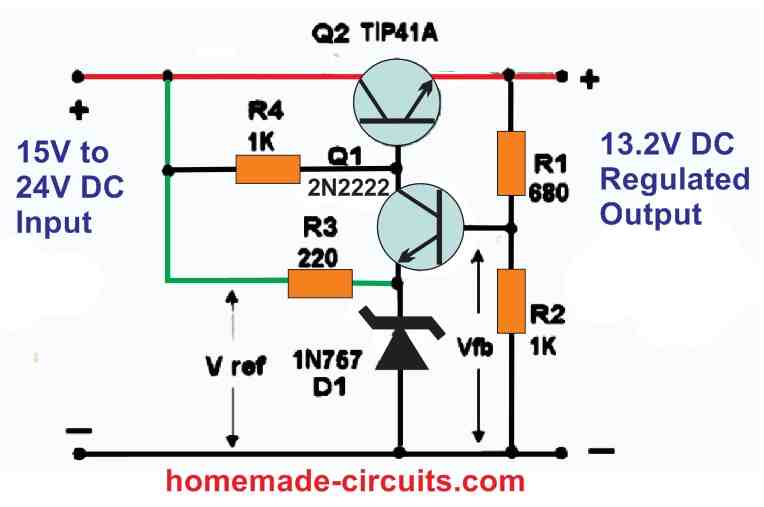
The drop across zener diode D1 holds the emitter of Q1 at a set and regulated voltage. The bias current from R3 and the emitter current from Q1 cause this dip.
This drop is generated by R3's bias current and Q1's emitter current.
If the output voltage drops, Q1 would be switched off, allowing less current to flow via bias resistor R4.
The collector voltage will increase, enhancing the voltage at the base of pass transistor Q2 and, hence, the emitter of Q2, that tends to be the power supply regulator's output terminal.
This voltage increase will be sent to the base of Q1, compensating for the original dip. The total impact will result in an increased output voltage stability.
100% Perfection is not Possible
This adjustment, however, is not the ideal one. The regulator circuit is a limited gain feedback amplifier.
Because the voltage gain is mostly provided by Q1, the circuit could have a net open-loop voltage gain of may be around 20-100, depending on Q1 gain, power supply load, zener diode impedance, and other parameters.
Loop gain can be defined as the product of total gain multiplied by the feedback factor.
In this situation, the feedback factor is the ratio R2 /(R1 + R2). Everything else being equal, the greater the loop gain, the better the regulation.
In reality, this circuit will offer a 10X or greater enhancement in regulation compared to the earlier circuits. However, t his circuit has certain restrictions, a few of which are as follows:
- In Q1, the output voltage cannot be lower than the zener voltage + the base-emitter loss.
- There is no current limiting or short-circuit protection. Since there will always be a voltage loss across R4, the maximum regulated output voltage is restricted.
- Because the feedback factor R2 /(R1 + R2) declines with increasing output voltage, regulation becomes gradually worse.
- Because part of the bias currents (via R3 and R4) originate from the unregulated side, the output would be impacted by fluctuations in the input voltage, worsening regulation.
These issues could be resolved with circuit adjustments and with the installation of a few additional components.
The first problem can be solved by using a low voltage zener diode, even though the best reliable zeners are approximately 5 to 8 volts.
It is feasible to utilize a secondary floating power supply circuit to deliver voltages below (negative) ground and transfer R2 to a negative voltage rather than ground.
Connect a resistance to the input, and the voltage drop across it can work as a function of load current which can influence the regulator output.
Extra open-loop gain could be obtained by using additional transistors or an op-amp.
Advantages of Common Emitter Regulator with Feedback
This configuration works better compared to a Darlington Pair emitter follower based regulators due to its reduced voltage drop across the input/output terminals.
The voltage drop attained from these designs is barely around 0.65 volts, which contributes to greater efficiency, and empowers the circuit to work effectively regardless whether or not the un-stabilized input voltage is only some hundred millivolts above the expected output voltage.
Battery Eliminator using Series Regulator Circuit
The indicated battery eliminator circuit is a functional illustration of a design built using a basic series regulator.
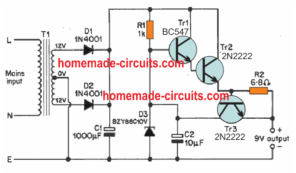
The model is developed for all applications working with 9 volt DC with a maximum current not exceeding 100 mA. It isn't appropriate for devices that demand a relatively higher amount of current.
T1 is a 12 -0 - 12 volt 100 mA transformer which supplies isolated protection isolation and a voltage step-down, while its center tapped secondary winding operates a basic push-pull rectifier with a filter capacitor.
With no load the output will be around 18 volts DC, which may drop to approximately 12 volts at full load.
The circuit that works like a voltage stabilizer is actually a basic series type design incorporating R1, D3 and C2 in order to get a regulated 10 V nominal output.
The zener current ranges through around 8 mA without load, and down to about 3 mA at full load. The dissipation generated from R1 and D3 asa result is minimal.
A Darlington pair emitter follower formed by TR1 and TR2 can be seen configured as the output buffer amplifier delivers a current gain of about 30,000 at full output, while the minimum gain being 10,000.
At this gain level whn the unit operates using 3 mA under full load current, and a minimum gain i exhibits almost no deviation in the voltage drop across the amplifier even while the load current fluctuates.
The real voltage drop from the output amplifier is approximately 1.3 volts, and with a moderate 10 volt input this offers an output of roughly 8.7 volts.
This looks almost equal to the specified 9 V, considering the fact that even the real a 9 volt battery may show variations from 9.5 V to 7.5 V during its operational period.
Adding a Current Limit to a Series Regulator
For regulators explained above it normally becomes important to add an output short circuit protection.
This may be necessary so that the design is able to deliver a good regulation along with a low output impedance. Since the supply source is very low impedance a very high output current can pass in the situation of an accidental output short circuit.
This might cause the output transistor, along with a few of the other parts to get immediately burned.
A typical fuse may simply fail to offer sufficient protection because the harm would likely occur quickly even before the fuse could possibly react and blow.
The easiest way to implement this perhaps by adding a current limiter to the circuit. This involves supplemental circuitry without any direct impact to the performance of the design under normal working conditions.
However the current limiter might cause the output voltage to drop quickly if the connected load tries to draw substantial amounts of current.
Actually the output voltage lowers so quickly, that despite having a short circuit placed across the output the current available from the circuit is a bit more than its specified maximum rating.
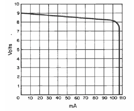
The outcome of a current limiting circuit is proven in the data below which displays the output voltage and current with regard to a progressively lowering load impedance, as attained from the proposed Battery Eliminator unit.
The current limiting circuitry works by using only a couple of elements; R2 and Tr3. Its response is actually so quick that it simply eliminates all possible risks of short circuit at the output thereby providing a fail proof protection to the output devices. The working of the current limiting can be understood as I have explained below.
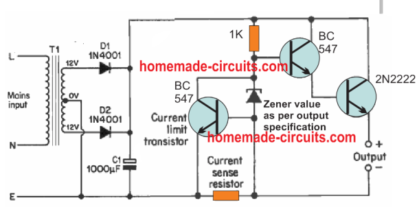
R2 is wired in series with the output, which causes the voltage developed across R2 to be proportionate to the output current.
At output consumptions reaching 100 mA the voltage produced across R2 won't be enough to trigger on Tr3, since it is a silicon transistor requiring a minimum potential of 0.65 V to switch ON.
However when the output load exceeds the 100 mA limit, it geneartes enough potential across T2 to adequately switch ON Tr3 into conduction.
TR3 in turn causes some current fto flow towards Trl across the negative supply rail through the load.
This results in some reduction of the output voltage. If the load increases further results in a proportionate rise in potential across R2 to rise, forcing Tr3 to switch ON even harder.
This consequently allows higher amounts current being shifted towards Tr1 and the negative line through Tr3 and the load. This action further leads to a proportionately rising voltage drop of the output voltage.
Even in case of an output short circuit, Tr3 will likely be biased hard into conduction, forcing the output voltage to drop to zero, ensuring that the output current is never allowed to exceed the 100 mA mark.
Another Voltage Regulator Circuit Project with Current Limiting
The next figure below depicts one way for incorporating current limiting with a voltage regulator circuit. Resistor R4 is connected in series with a PNP transistor, Q1, which serves as a current source.
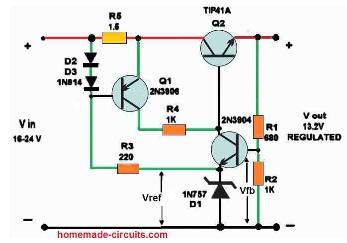
This resistor is required to restrict the current sent to D1. At the base of Q1, diodes D2 and D3 generate a very constant voltage which is 1.4 volts lower than the regulator input voltage.
Q1 conducts so long as the voltage drop caused by the pass -transistor collector current is less than around 0.7 volts across sampling resistor R5. As the load current builds, the drop over R5 rises to the extent where it begins to cut off Q1.
R4 can now force the base voltage of pass transistor Q2 to drop, causing the regulator output voltage to decrease.
Because this current also biases reference zener diode D1, the reference voltage falls, lowering the output voltage. The current taken from the regulator could thus be limited in this manner.
A 0.7 volt drop across R5 will initiate current limiting, hence R5 should have a value of 0.7 /(Current Limit), or around 0.7 ohms for 1 amp, 0.35 ohms for 2 amps, and so on.
Precision Voltage Regulator Using an Op Amp
The figure below shows how an op-amp can be introduced in a linear voltage regulator circuit to enhance control.
Take note that the gain will now increase drastically.
Nevertheless, frequency correction will almost certainly be required in certain circumstances, as loop phase shift may produce oscillation under some or all stages of loading.
Although the bias for the op-amp can be supplied from the regulator directly, an additional auxiliary low-power supply is usually desirable.
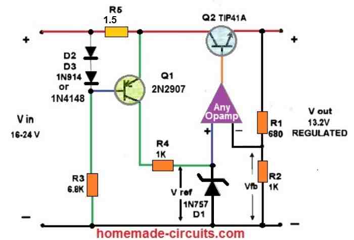
A negative source may be required for the op-amp, particularly in case the regulator is intended to be adjustable or to swing down to zero volts output, as in a laboratory power supply.
Simple Switchable Voltage Regulator Circuit
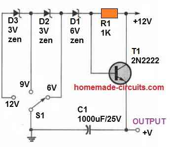
Referring to the figure above, it is possible to build a three-step voltage controlled supply by combining three Zener diodes in series with a switch and with a few other readily accessible components.
The power supply can be a 12V or a 15 volts DC.
When switch S1 is set to the 6 volt mode, the 6V DC from the supply source passing via resistor R1 biases input transistor T1. The same 6V is replicated at the circuit output.
Since T1 is configured as an emitter follower, the forward voltage of the transistor base/emitter leads which is 0.6 V will be deducted from the 6V, and the final output will be 6 - 0.6 =5.4 V.
The output is increased by 3 volts when a 3-volt Zener (D2) is introduced to the circuit when the switch S1 is moved to the 9-volt position.
By including a second 3 volt Zener, the transistor will be biased at 12 volts when the switch is pushed to the 12 volt position. The circuit's output is filtered by capacitor C1.
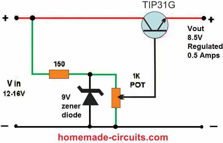
Variable Regulated Bench Power Supply Circuit Project
Variable voltage stabilized power supplies work with similar principle like the fixed voltage regulator types, but they feature a potentiometer control which facilitates a stabilized output with a variable voltage range.
These circuits are best suited as bench and workshop power supplies, although they can also be used in applications that demand different adjustable inputs for the analysis.
For such jobs the power supply potentiometer acts like a preset control that can be used to tailor the output voltage of the supply to the desired regulated voltage levels.
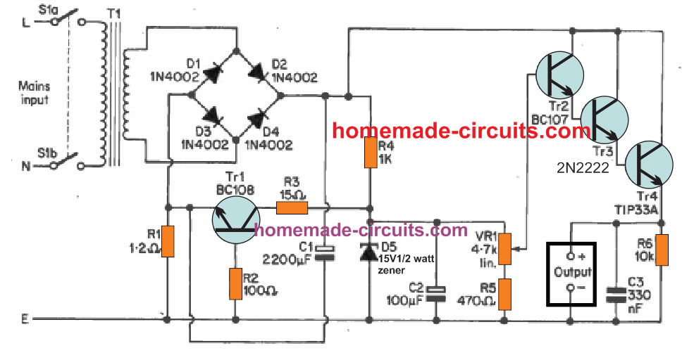
The figure above shows a classic example of a variable voltage regulator circuit which will provide a continuously variable stabilized output from 0 to 12V.
Main Features
- The current range is limited to a maximum of 500 mA, although this can increased to higher levels by suitably upgrading the transistors and the transformer.
- The design provides a very good noise and ripple regulation, which may be less than 1 mV.
- The maximum difference between the input supply and the regulated output is not more than 0.3 V even at full output loading.
- The regulated variable power supply can be ideally used for testing almost all types of electronic projects with require high quality regulated supplies.
How it Works
In this design we can see a potential divider circuit included between the output zener stabilizer stage and the input buffer amplifier.
This potential divider is created by VR1 and R5. This enables the VR1's slider arm to be adjusted from a minimum 1.4 volts when it is near the base of its track, up to 15 V zener level while it is at the highest point of the of its adjustment range.
There exists roughly 2 volts dropped over the output buffer stage, allowing an output voltage range from from 0 V to around 13 V.
Having said that, the upper voltage range is susceptible to part tolerances, like the 5% tolerance on the zener voltage. Therefore the optimum output voltage might be a shade higher than 12 volts.
A few types of efficient overload protection circuit can be very important for any bench power supply. This may be essential since the output may be vulnerable to random overloads and short circuits.
We employ a rather straightforward current limiting in the present design, determined by Trl and its linked elements.
When the unit is operated with normal conditions the voltage produced across R1, which is attached in series with the supply uotput, is too little to trigger Trl into conduction.
In this scenario the circuit works normally, besides a small voltage drop genearted by R1. This produces hardly any effect on the regulation efficiency of the unit.
This is because, the R1 stage comes before regulator circuitry. In an event of an overload situation, the potential induced across R1 shoots up to around 0.65 volts, which forces Tr1 to switch ON, on account of the base current acquired from the potential difference generated across the resistor R2.
This causes R3 and Tr 1 to draw a significant amount of curent, causing the voltage drop across R4 to increase substantially, and the output voltage to be reduced.
This action instantly restricts the output current to a maximum of 550 to 600 mA despite of the short circuit on the output.
Since the current limiting feature restricts the output voltage to practically 0 V.
R6 is rigged like a load resistor which basically prevents the output current from getting too low and the buffer amplifier unable to work normally. C3 allows the device to achieve an excellent transient response.
Drawbacks
Just like any typical linear regulator, the power dissipation in Tr4 is determined by the output voltage and current and is at a maximum with pot adjusted for lower output voltages and higher output loads.
In most severe circumstance there may be possibly 20 V induced across Tr4, causing a current of around 600 mA to flow through it. This results in a power dissipation of around 12 watts in the transistor.
To be able to tolerate this for long durations the device must be installed on a rather big heatsink. VR1 could be installed with a sizeable control knob facilatating a scale calibrated displaying the output voltage markings.
Parts List
- Resistors. (All 1/3 watt 5%).
- R1 1.2 ohms
- R2 100 ohms
- R3 15 ohms
- R4 1k
- R5 470 ohms
- R6 10k
- VR1 4.7k linear carbon
- Capacitors
- C1 2200 µF 40V
- C2 100 µF 25V
- C3 330 nF
- Semiconductors
- Tr1 BC108
- Tr2 BC107
- Tr3 BFY51
- Tr4 TIP33A
- DI to D4 1N4002 (4 off)
- D5 BZY88C15V (15 volt, 400 mW zener)
- Transformer
- T1 Standard mains primary, 17 or 18 volt, 1 amp
- secondary
- Switch
- S1 D.P.S.T. rotary mains or toggle type
- Miscellaneous
- Case, output sockets, circuit board, mains lead, wire,
- solder etc.
3.3V, 5V Voltage Regulator Circuit with Diodes and Transistors
A quick and a clean way to derive a 3.3V or 5V regulation or any other desired value from a given higher voltage source is to use series diodes as shown in the following diagram.
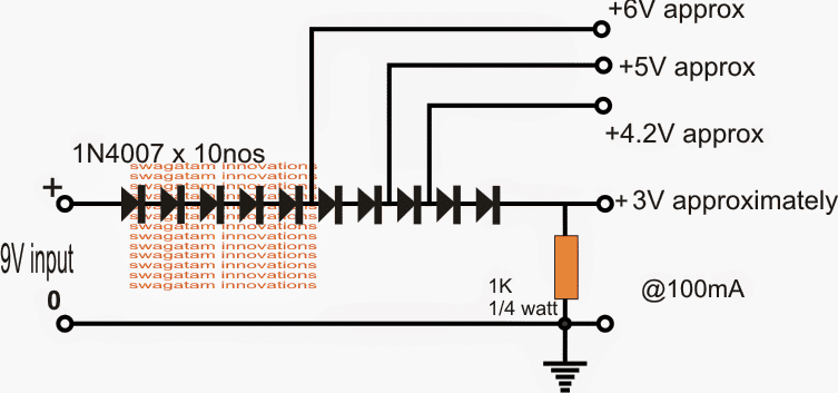
Using Rectifier Diodes for Dropping Voltage
In the above diagram we can see about 10 diodes being used for acquiring a 3V output at the extreme end, while other corresponding values can also be seen in the form of 4.2v, 5v and 6V levels across the relevant dropping diodes.
We know that typically a rectifier diode is characterized to drop around 0.6V across itself, meaning any potential fed at a diode's anode will generate an output at its cathode which would be normally approximately 0.6V less than the input at its anode.
We take the advantage of the above feature in order to achieve the indicated lower voltage potentials from a given higher supply.
Using 1N4007 Diode for 1 Amp Current
In the diagram 1N4007 diodes are shown which might yield not more than 100mA, although 1N4007 diodes are rated to handle upto 1amp, it needs to be ensured that the diodes do not begin warming up, otherwise that would result in higher voltages being allowed to pass.
Because as the diode heats up the rated drop across it begins receding towards zero, that's why not more than a 100mA max should be expected from the above design for preventing over heating and enabling an optimal response from the design.
For higher currents one may opt for higher rated diodes such as 1N5408 (0.5amp max) or 6A4(2amp max) etc.
The drawback of the above design is that it does not produce accurate potential values at the output and therefore might not be suitable for applications where customized voltage references may be needed or for applications where the load parameter could be crucial in terms of its voltage specs.
For such applications the following configuration could become very desirable and useful:
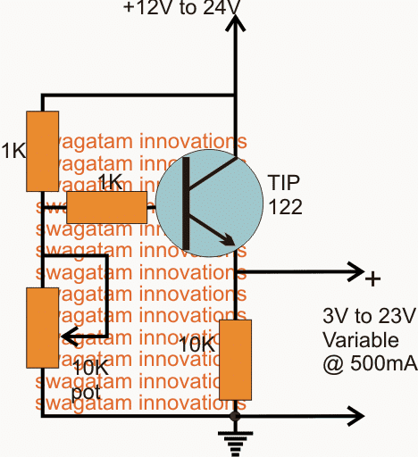
Using an Emitter Follower BJT
The diagram above shows a simple emitter follower configuration using a BJT and a few resistors.
The idea is self explanatory, here the pot is used for adjusting the output to any desired level right from 3V or lower to the maximum fed input level, although the maximum available output would be always less than 0.6V than the applied input voltage.
The advantage of incorporating a BJT for making 3.3V or 5V regulator circuit is that it enables you to achieve any desired voltage using minimum number of components.
It also allows higher current loads to be used at the outputs, moreover the input voltage has no restrictions and may be increased as per the BJT's handling capacity and by some minor tweaks in the resistor values.
In the given example, an input of 12V to 24V can be seen, which can be tailored to any desired level such as to 3.3V, 6V, 9V, 12V, 15V, 18V, 20V or to any other intermediate value simply by flicking the knob of the included potentiometer.
5V Stabilized Regulator
The working of the 5V transistor regulator circuit is as follows.
The 1k resistor attached between the collector/base of transistor BD131 typically means that the BD131 always stays in the conducting mode.
However the 4.3 V zener diode ZD1 clamps the base voltage of the transistor 2N697 to approximately 4.3 volts lower than the emitter voltage of the BJT BD131.
The 2N697 begins turning ON as soon as its base voltage reaches around 0.6 V positive with respect to its emitter voltage, and at this point the BD131 emitter reaches a potential of around 4.9 V positive.
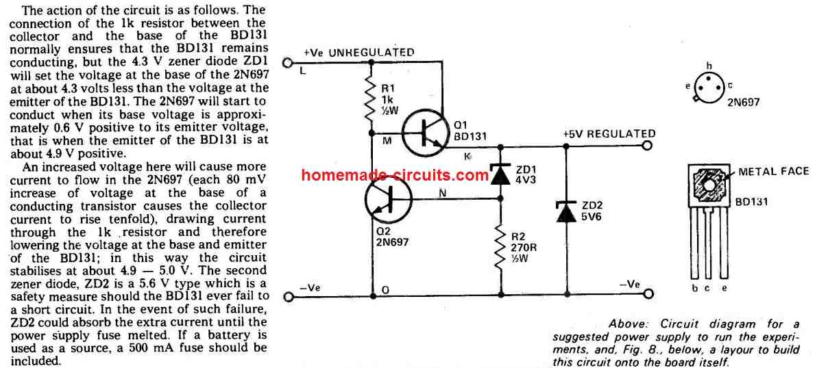
An elevated voltage at this point allows higher amount of current to flow through the 2N697 (every 80 mV rise at the base of a conducting transistor enables the collector current to increase by 10 times value), causing the transistor to pull more current by means of the lk resistor which consequently decreases the base/emitter voltage of the BD131.
By doing this the circuit ensures proper stabilization at approximately 4.9 V - 5.0 V. Another zener diode, ZD2 has a value of 5.6 V positioned for the safety in case the BD131 malfunctions causing a short circuit.
In that situation, ZD2 may possibly absorb the excess current until the attached fuse blows. If the circuit is operated with a battery, a 500 mA fuse should be just fine.
How to Stop Transistor Overheating at Higher input/Output Differentials
The pass transistor type regulators as explained above usually encounters the situation of experiencing extremely high dissipation appearing from the series regulator transistor whenever the output voltage is a lot lower than the input supply..
Each time a high output current is driven at low voltage (TTL) it might possibly be crucial to employ a cooling fan on the heatsink.
Possibly an severe illustration may be the scenario of a source unit specified of providing 5 amps through 5 and 50 volts.
This type of unit could have normally a 60 volt unregulated supply. Imagine this particular device is to source TTL circuits in its entire rated current. The series element in the circuit will have to in this situation dissipate 275 watts!
The expense of delivering sufficient cooling appears to be realized only by the price of the series transistor.
In case the voltage drop over the regulator transistor could possibly be limited to 5.5 volts, without depending on the preferred output voltage, the dissipation could be substantially decreased in the above illustration this may be 10% of its initial value.
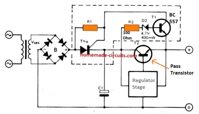
This could be accomplished by employing three semiconductor parts and a couple of resistors (figure 1). Here's how exactly this works: thyristor Thy is allowed to be conductive normally through R1.
Nevertheless, once the voltage drop across T2 - the series regulator goes beyond 5.5 volts, T1 begins to conduct, resulting in the thyristor to `open' at the subsequent zero-crossing of the bridge rectifier output.
This specific working sequence constantly controls the charge fed across C1 - the filter capacitor - in order that the unregulated supply is fixed at 5.5 volts over the regulated output voltage. The resistance value necessary for R1 is determined as follows:
R1 = 1.4 x Vsec - (Vmin + 5) / 50 (result will be in k Ohm)
where Vsec indicates the secondary RMS voltage of the transformer and Vmin signifies the minimum value of the regulated output.
The thyristor has to be competent at withstanding the peak ripple current, and its functioning voltage should be a minimum of 1.5 Vsec.
The series regulator transistor should be specified to support the highest output current, Imax, and should be mounted on a heatsink where it may dissipate 5.5 x Isec watts.
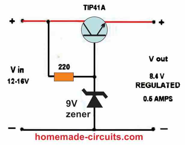
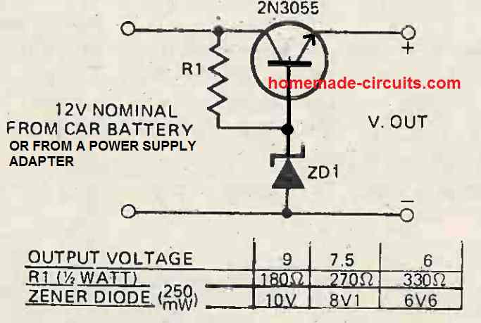
Getting Fixed Voltage from Transistor Regulator
Using just a single transistor and few zener diodes, you can get different voltages ranging from 5 V to 10 V from a supply input of 12 V.
The below shown diagram, and the chart shows how the transistor, the zener diode, and the biasing resistor can be configured for implementing the simple transistor regulator circuit.
Conclusion
In this post I have explained how to build simple linear voltage regulator circuits using series pass transistor and zener diode.
Linear stabilized power supplies provide us with fairly easy options for creating fixed stabilized outputs using minimum number of components.
In such designs, basically an NPN transistor is configured in series with positive input supply line in a common emitter mode. The stabilized output is obtained across the emitter of the transistor and the negative supply line.
The base of the transistor is configured with a zener clamp circuit or a adjustable voltage divider which ensures that the emitter side voltage of the transistor closely replicates the base potential at the emitter output of the transistor.
If the load is a high current load, the transistor regulates the voltage to the load by causing an increase in its resistance and thus ensures that the voltage to the load does not exceed the specified fixed value as set by its base configuration.
This concludes our article on simple voltage regulator circuits and projects. If you have any queries or modifications related to the above concepts please feel free to comment below for quick replies.


Comments (28)
Hi
I need info please. Its for a voltage regulator where the input do vary between 12v dc and 100v dc. but the out put must be regulated to 24 volts.
I know the 12v input part is a bit low, but its not a problem for me. Its just the part above 24v dc that needed to be regulated.
I don’t know if you can help me with a link, a schematic or even an ignore, all will help.
Thanks
Abdul, if you want to use a linear regulator then it will heat up a lot when the input is 100V. Here’s a simple linear design. Here ZX should be 24V rated to keep the output fixed at 24V, as long as input is above 24V.
Hi Swagatam, I am looking for a circuit to regulate 13.8 V DC, from a power supply, down to 12.5 V DC at 7 A. This is to supply a VHF RF power module. Thanks for any help.
Hi Joy,
If your source 13.8V is rated to provide 7 amps, then you can drop the voltage using just a couple of 10 amp diodes in series….
Thank you for your reply. However, I was thinking of a more robust linear circuit, like an LDO voltage regulator with a pass transistor. Of course an LM117 won’t work because it needs a 3 V overhead and I have only a 1.3 V differential to work with. The 13.8 V power supply is capable of 25 A. I know more modern day LDO voltage regulators need only 0.9 V differential, but I am not sure of the lash up needed. Thanks again for any suggestions.
Sure, in that case you can try one of the circuits from this article:
https://www.homemade-circuits.com/low-dropout-5v-12v-regulator-circuits-using-transistors/
Hi Swagatam, I have a circuit similar to the very last schematic with the 2n3055, except it has a resistor in place of ZD1, how do I calculate both resistor values or can you recommend a tutorial, many thanks, Mike.
Hi Mike,
You can use the following voltage divider formula for getting the values of both the resistors:
https://www.homemade-circuits.com/voltage-divider-calculator-software-potential-divider-calculator/
For the output voltage make sure to add +1V extra in the field, to compensate the forward drop of the transistor.
For example if the desired output voltage is 12V, then use 12 + 1 = 13 for the output voltage field.
hi swagatam

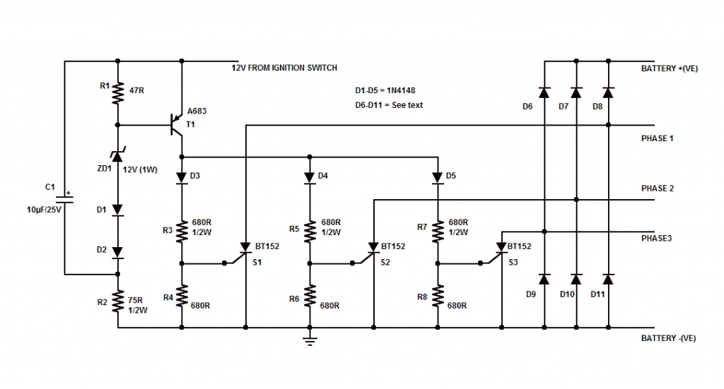
i found this series 3 phase regulator for motorcycle
is this scheme reasonable and safe to implement?
Do you have any corrections to this scheme?
greetings from indonesia
Hi ghozheider, the circuit looks good but it can be simplified using lesser number of parts as shown in the following diagram:
Hi Swagatam, I have some questions about Voltage Regulator from 12V to 9.0 Volts, for currents up to 2000 mA.
Could we connect via Zoom, so that I can pick your brains on this?
Hi Neri,
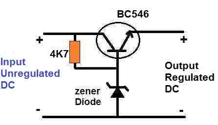
You can try the following circuit for getting a 9V from a 12V input:
Please replace the BC546 with a TIP142 transistor, and the zener diode with a 10V zener diode.
Please feel free to discuss your queries through this blog, i will be most happy to help!
Load resistor=(12-5)/0.02 =35ohms/wattage=(12-5)=0.14wattage or 1/4amps
I decided to give this page a look and build a discrete linear regulator using the schematic for the BD131 and the 2N697 with the 4.3v Zener which would give me a solid +5v supply for a project. Now I could have just gone and used an LM340T-5 and a limited list of other pieces but what fun is that? So, it took a little digging and a really neat cross reference page I just found, on it, it wasn’t a direct cross over to get here but instead of the BD131 I’m going to use a TIP31C and for the 2N697, the good old 2N2222 comes in and by going from the 2N607 to another number and from that number it goes to another which matches my 2N2222. How about that? Let me give it a whirl. I only need a circuit that will supply 600 or less milliamps as far as I can see, and at the moment I’m including a 600 mA poly fuse on the input line. I’m going to add in the 5.6 V Zener on the output for added safety along with some smoothing caps and such along with a few other components to give me some indication of how the circuit is working in the project. I got to say this Swagatam, your pages are AWSOME. They give me so many ideas and information. This Vreg will be included in an Inverter circuit I’m working on using the EGS002 Sinewave generator to drive some converter boards, hopefully I can make this setup as an expandable hot swap modular system. It will be using a few double sided proto boards for the first run along with some PCB’s found on Ebay. This is going to be interesting and I sure hope it works as I want to set myself up so I can go back off the grid without spending as much money as I did the first time, aside from building my Battery bank. I’m hoping I can do that with a combination of wet cells and LiPo’s. That may not be a good idea though in the end. Any input is welcome.
Thank you Bret, Glad the article helped! Yes, the mentioned transistors can definitely work for the designs explained above. The only issue with these linear regulators is the high dissipation rate in response to an increasing input/output voltage difference.
I hope you are able to succeed with the project. All the best to you!
Yes pretty much any type of Vreg is going to have its loses as heat as current requirements increase. Using components that have higher capacity and gain is about the only thing a person can do to limit loses, then keeping component count down so as not to have each one reducing efficiencies. Resistance is a key factor in the complete circuit. One needs transistors thapt have minimal impedance.
You are absolutely right, thanks for your feedback!
Hello, good afternoon, my name is Carlos. I need a circuit to test all kinds of zener diodes and be able to know their value….. Would you have that circuit? Thank you very much.
You can find a schematic for building a Zener tester online by searching that topic easily enough. I used that have a tester that would work for about anything up to around ~60v depending on how fresh the 9v bat was. It had a button switch for checking the Zener voltage and also the loaded voltage, used a 10k and a 22k R, a 555 with associated components for the timer as a 100k freq gen feeding a diode to make a half wave pulse to a small audio impedance X-former. I added an LCD meter for reading the Z voltage instead of using a multi meter. Since that tester used a meter with an isolated supply it needed 2 9v’s but there are meters out there that can use a common supply so that would reduce cost and complexity some. One way would use a Double pole switch obviously. That circuit is online but finding an X-former with the 8 ohm x 10k is getting pretty tough these days and they are pricey when you do find them. Last time I found a listing for one of these was from a place in Australia but they were currently out of stock which was a bummer because I don’t have the tester anymore, I want to build it again, I have most of the circuit on a board but that X-former is my hold up now. I have another tester I started building that uses a buck boost board from a source online( Ebay) a DC/DC unit that converts battery V to and adjustable output that would be great for basically the same type and works up to around the same voltage maybe a bit more. This circuit uses an ATtiny85 to run an OLED display I think, I’ve had it put away for so long now unfinished, I forget a some things about that project. Either way, circuits for this are out there and I’m pretty Swagatam has a posting on this topic.
Thank you Bret,
I think the 555 based circuit which can be found online is the easiest zener diode tester circuit you can build at home:
Hello Carlos,
You can build the first circuit from the above article. You can use 4k7 for the load resistor, and upto 24V as the input voltage. For the zener diode you can connect any unknown zener diode and then measure the output voltage with a voltmeter. The meter reading will provide the direct value of the zener diode.
Hi, Swagatam! Thanks for the great circuit explanations, as always!
Question: In the “Variable Regulated Bench Power Supply” circuit, the TR2 transistor (BC107) is a pretty old component that is hard to get here in the USA. The TR3 transistor (2N2222 or BFY51) is also hard to get in the USA. These two transistors are older style transistors in a TO-39 metal can case. TR2 and TR3 should not have to handle a lot of current. These two transistors just increase the gain of TR4. The TIP33A power transistor is the “pass” transistor that has to handle the majority of the current in the circuit. Can I safely use a 2N3904 transistor for TR2 and TR3? The 2N3904 has good gain (about 200) and is easy to obtain here in the USA. Two of them, in the “triple Darlington” configuration of this circuit, ought to increase the gain A LOT before the gain is further multiplied by the TIP33A.
Thanks in advance!
– Brock
Thank you, Brock, you are right, you can replace those with any small signal, general purpose NPN transistor of your choice, without any issues.
which regulator circuit is best for use in tube equipment. i need a 125 vdc reg output w/a max of 150 vdc on the input. current draw is 200 ma or less
barry
Here’s a nifty little constant-current circuit snippet. It’ll keep pumping the same amount of current as downstream voltage rises, until the current naturally just can’t flow that fast.
It uses one NPN transistor, one PNP transistor, one n-jfet and one p-jfet. That’s it!
The top circuit snippet in the link below is the old-style (adjustable) current limiter I was using. The bottom one is described above. The top circuit snippet has been set to the same starting current as the bottom one, for comparison purposes.
http://tinyurl.com/y2y4ln5o
Hey, just wondering if you are trying to promote falstad website?
Is any voltage regulator ckt without zenor diode
You can replace the zener with a of 78L05 IC