In this post I have explained some basic facts about DC to DC buck converters and also learn how to build a simple buck converter circuit. A buck converter is also popularly known as a step-down converter, since its basic function is to step down a higher input voltage level to a lower output voltage level, with high efficiency.
The practical buck converter circuit explained here uses only 3 transistors and is extremely easy to build. Even though the circuit is simple, it has a high efficiency.
The circuit can be used to drive 3.3 V LEDs from a higher input supplies such as from 12 V, or 9 V supply inputs.
The buck converter design can be also easily upgraded to operate higher rated loads instead of an LED.
Advantages of Buck Converters Compared to Linear Regulators
The main advantage of a DC to DC buck converter compared to a linear regulator is that buck converters are hugely efficient than linear regulators.
Linear regulators such as IC 7812, IC 7805, LM317, LM338 waste a lot of energy through heat dissipation, whereas heat dissipation in buck converters is minimal.
Due to minimal heat dissipation, a heatsink may not be required in buck converters, or this may be very small in size.
The efficiency of linear regulators may range between 25% and 50%, the efficiency of buck converters is mostly around 90%.
Basic Working of a Buck Converter Topology
Referring to the figure below, let's try to understand how a 'buck' or a 'step-down' converter works. With a buck converter circuit, a higher input voltage can be transformed into a lower output voltage. Its basic mode of operation is described as follows.
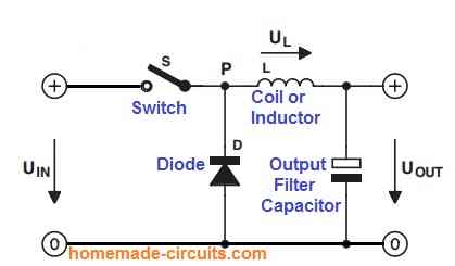
As soon as switch S is pressed, a positive voltage develops across the inductor L. This is because UIN is higher than Uout. The coil initially tries to resist the instantaneous current flow. As a result, the current in the coil increases linearly, and energy begins storing in the coil.
Next, as soon as switch S is opened, the stored current flows through the coil into the output capacitor through diode D.
Since the voltage UL across the coil is now negative, the current through the coil reduces linearly. The output receives the energy that was captured and stored in the coil. Now, if Switch S is closed once again, the procedure begins afresh and keeps repeating as the switch is operated ON/OFF.
Modes of Operation
The voltage that appears at the output is determined by how the switch S is operated. According to figure below, there are three basic types of current flow.
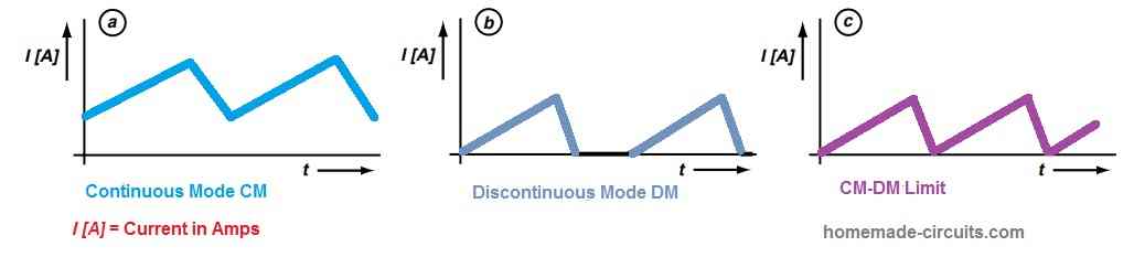
- Referring to the figure (a) above suppose, the switch S is closed and opened such that the current flowing inside the coil isn't able to reach zero. In this situation a constant flow of current will be experienced through the coil. This is referred to as "continuous mode" (CM).
- Now let's imagine the switch S is closed and opened such that current is able to reach zero for part of the cycle, as illustrated in Figure (b). Then the circuit can be assumed to be operating in 'discontinuous mode' (DM).
- In the third scenario if suppose the switch is closed and opened such that the coil current is able to exactly reach zero as shown in figure (c), then we call this as CM/DM limit operation.
This means that, in a buck converter both the output voltage and power could be varied by adjusting the "on" periods of the switch. This is also called the mark-space ratio.
That's enough theory; now let's examine a straightforward real-world circuit.
Making a Practical Buck Converter Design
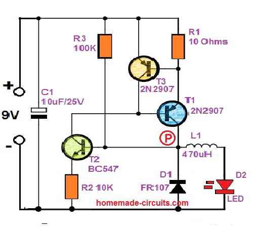
The following figure shows a simple practical DC to DC buck converter circuit using only 3 transistors and a few other passive elements.
It works in the following manner:
Switch S in this circuit is represented by transistor T1. The other components of the step-down converter are diode D1 and coil L1.
As soon as the circuit is powered, R3 supplies a base current to T2 (because D2's forward voltage spec is larger than 0.7 V) and T2 is switched ON.
With T2 conducting, T1 gets a base bias and it also begins conducting. In this situation, point P experiences an increase in voltage, which causes T2 to conduct even harder.
Now as point P's voltage reaches 9 V, the current through L1 starts to increase. The voltage across the coil and its inductance both influence how quickly the current inside it increases.
As the current across the coil increases, the voltage across R1 decreases. As soon as this potential hits 0.7 V (about 70 mA) causes T3 to turn ON. This quickly removes the base current of T1.
Since the current in L1 can now no longer increase, the voltage at point P starts to decrease. T2 as a result is switched off, followed by T1.
The current via L1 now travels via D1 until it drops to zero. This causes the voltage on T2 to increase again, and the process repeats afresh.
The transistors work as a thyristor with positive feedback, resulting in an oscillation. T3 makes sure that T1 is shut off at the predetermined current and that the circuit operates in CM/DM limit mode.
Upgrading the Circuit for Higher Loads
Instead of illuminating an LED, you could employ this circuit to operate a higher rated load. But with a higher load you will find the buck converter not oscillating.
This is due to the load preventing R3 from turning on T2 at startup.
This issue may be avoided by placing a capacitor (0.1uF) between point P and the base of T2.
Another smart move would be to smooth the voltage by connecting a 10 F electrolytic capacitor across the output.
The buck converter functions as a current source instead of a voltage source and is unregulated. However, for most straightforward applications, this will be more than sufficient.
Simple Two Transistor Buck Converter Circuit
Parts List
- All resistors are 1/4 watt 5%
- R1 = 470 Ohms
- R2, R4 = 100 Ohms
- R3, R5 = 2.2 K
- Capacitors
- C1, C3 = 1000 uF/ 25 V
- C2 = 220 uF / 25 V
- Semiconductors
- D1 = FR107
- D2 = 12 V 1 watt Zener diode
- T1 = 2N2907
- T2 = BC547
- L1 = 120 uH
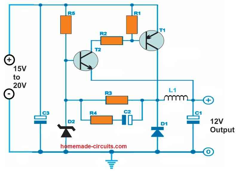
We can make the above design much simpler using just two transistors? Referring to the circuit diagram above, we can see a regulated step-down converter, which can generate 12 V DC from a 20 V DC. The main components of this design are transistor T1, diode D1 and coil L1.
The circuit works using the feedback between a combination of the PNP/NPN transistors. Here, the working of T1 is not dependent on the maximum coil current. Instead it is determined by the RC network of R4/C2.
The voltage regulation for this simple buck converter circuit is determined by the zener diode D2, associated with the emitter of T2.
This DC to DC buck converter design is highly efficient, which may be as high as 90%.
How to Build
- Step#1: Take 20 mm by 20 mm general purpose strip board.
- Spep#2: Clean the copper side with a sand paper.
- Step#3: Take the resistors and the diodes and bend their leads leaving 1 mm distance between their body and the leads.
- Step#4: Insert the resistors into the PCB and solder them. Cut the excess lead lengths.
- Step#5: Insert the transistors as per the same layout position as indicated in the schematic. Solder their leads, and trim the extended leads.
- Step#6: Now, insert the inductor, solder it, and trim its leads.
- Step#7: Finally insert, the capacitor and the LED, solder the leads. Cut the excess leads
Once the above assembly is done carefully interconnect the leads of the various components by referring to the schematic diagram. Do this using the pieces of the trimmed lead wires, previously cut.
If you are unable to connect the leads directly from the copper side, you can use jumper wire from the component side of the PCB.
How to Test
- Keep the LED disconnected at the start.
- Apply 9 V DC to the circuit.
- Measure the voltage across the points where the LED is supposed to be connected.
- It must be around 3 V to 4 V.
- This will confirm that you have build the buck converter correctly, and it is working correctly.
- You can switch OFF power and connect the LED back in its position.
- Now switch ON the DC again, you will find the LED illuminated brightly from the 9 V DC input with maximum efficiency.
How to Measure the Efficiency
To measure the efficiency you can connect an ammeter in series with the positive line of the 9 V DC.
Then you can multiply the current reading with the voltage (9 V).
The result could be somewhere around 20% higher than the watt specification of the LED.
This might prove an 80% efficiency for the buck converter circuit, and likewise.
Adjustable PWM Buck Converter Circuit
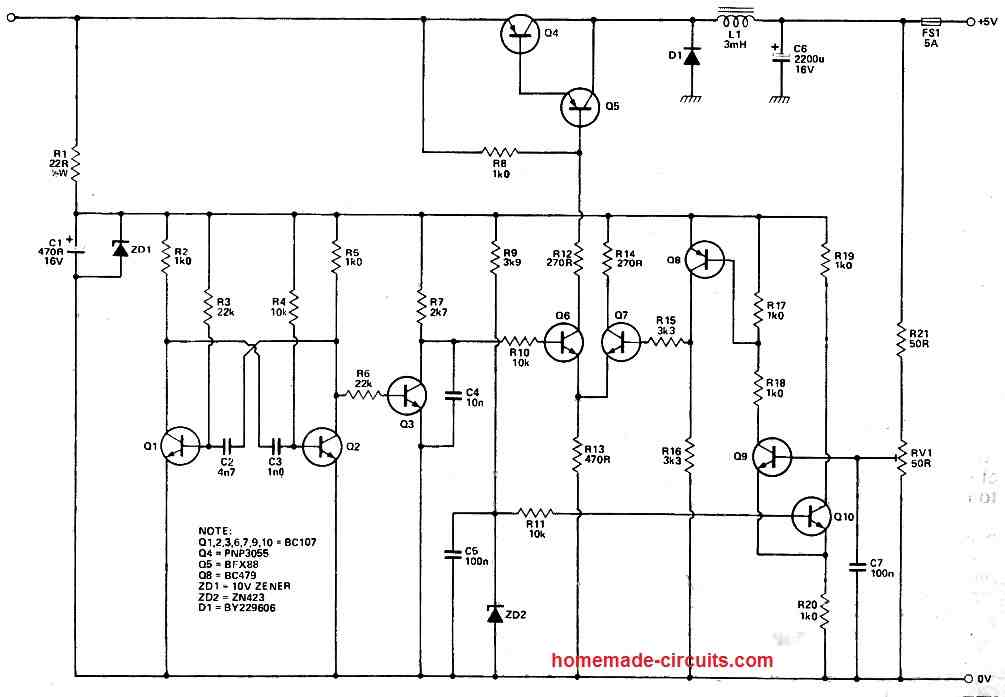
This circuit was initially designed with the purpose of generating a 5V power supply from a car battery to operate a BBC microcomputer.
Notably, the design refrains from employing integrated circuits (ICs), utilizing instead readily available discrete semiconductors salvaged from miscellaneous parts.
Efficiency Considerations
Achieving efficiencies surpassing 80%, this circuit outperforms linear regulators which generally exhibit maximum efficiencies ranging from 33% to 42%.
Astable Multivibrator and Pulse Generation
The operation commences with transistors Q1 and Q2 configured in an astable multivibrator arrangement.
This configuration yields a brief positive pulse at the base of Q3 at intervals of 50µs.
Consequently, the capacitor C4 discharges, subsequently recharging through the 2.7 kΩ resistor. This process delivers a gradually ascending voltage to the base of Q6.
Voltage Comparison and Regulation
Transistors Q9 and Q10 undertake a voltage comparison task, juxtaposing the reference voltage from the ZN423 with a segment of the regulator's output voltage.
This voltage slice derives from a potentiometer serving as the output voltage adjustment feature.
It's crucial to avoid substituting a zener diode for the ZN423, as the former's slope resistance reacts adversely to fluctuating battery voltages.
Adjustable Voltage Control and Pulse Width Modulation
As the potentiometer wiper voltage exceeds the reference voltage, Q8 activates.
Consequently, the ascending ramp at the base of Q6 must escalate to align with the voltage at the base of Q7.
This delay in activating the Darlington pair (Q4 and Q5) results in a narrower power output pulse to the choke.
This mechanism, known as pulse width modulation (PWM), in turn reduces the output voltage.
The nominal operating frequency is 20kHz, although it can vary considerably due to battery voltage fluctuations.
Output Stage and Energy Dissipation
The BY229-600 diode is specified for the catch diode, but in the prototype, a high-current rectifier proved effective.
The frequency of 20kHz seems manageable for these components.
Most wasted energy dissipates as heat in Q4, necessitating a suitable heat sink.
Output Voltage Feedback and Stability
The output voltage feedback attenuator incorporates 50Ω resistors to draw a minimum of 50mA from the output, essential for maintaining stability.
Alternatively, a 100Ω resistor could be shunted across the output, alongside a resistor and potentiometer (up to approximately 10kΩ each) to establish the correct feedback voltage.
When drawing 5A, a drop of 200mV in output voltage corresponds to an output resistance of 40 milliohms.
Grounding and Wiring
Designating the ground points with bold lines signifies their role as conduits for substantial currents.
These points necessitate robust connections, such as thick wiring or PCB tracks, tied back to a location proximate to the incoming battery's negative terminal.
This adherence to high-current grounding practices is a standard convention.
Output Regulation Strategies
The circuit does not currently encompass mechanisms for current limitation or crowbar protection.
Implementing a crowbar mechanism is straightforward, and current limiting can be achieved by manipulating Q9's base, thereby altering the power pulse's mark-space ratio.


Questions & Answers
Hi Swagatam,
I am so sorry to bother you with another of my questions as I am sure that you are very busy but I do not have anyone else that I can ask.
Some years ago I built a variable power supply from a kit, 0-30 volts 3 amps and it has served me well for a long time now. However I have always been disappointed with the coarsness of the voltage adjustment. The pots used are 10KA on both the voltage and current adjustments. When I need an accurate adjustment eg 3.3 volts I can never get closer that 1/10th of a volt each side of the target.
So I had an idea to replace the pots with 10 turn pots so I ordered a couple of 10K multi turn pots and fitted them both. It didn’t work how I expected it to. On the voltage pot I now go from 0 volts to 34 volts in less than a 1/2 a turn and the other 91/2 turns do nothing. I am now very puzzled.
Could you please try and explain where I have made a mistake and perhaps offer me a solution to my requirement?
Again I am very sorry to trouble you with my problem but I do hope that you can help me.
Thank you very much
Best regards.
Patrick
No problem Patrick,
I will try to help you!
If you are getting 0 to 34V in less than half a turn that means your pot range is not matching with the power supply circuit. It means 10K is a high value pot. To rectify this you can try using a 4.7K pot or a 2.2K pot. An ordinary linear pot should also work.
You can also try adding a 1K pot pot in series with the main pot. This additional pot can be used to make the coarse adjustments.
Hope this works for you.
Hi Swatam,
Thank you for your words of encouragement regarding the LM2576t-adj switching regulator. I will try and design a suitable PC board for an adjustable power suppl and see if I can get it to work. If you have the time and inclination then perhaps you could also design a 0-30 volt 3 amp adjustable power supply using this regulator and post it on your site. I am sure that it will be better and more efficient than mine. Slso I am certain that many people out there that frequent your site will have a great time building a laboratory grade power supply using this regulator as it looks much easier and a lot cheaper than a standard supply.
One more question if I may, For many years I have been receiving an email on my gmail account which informs me when you post a new circuit. Recently these emails have stopped coming. Have you stopped supplying this very valuable service or have I done something wrong? I would really like to continue to receive these notifications if at all possible. Please let me know when you can. Also when you reply to me it show on my gmail but it will not let me reply to you so I never know where to go to reply to you. Please help if you can.
Keep well and best regards
Patrick
It’s my pleasure Patrick, I will certainly think about writing an article describing how to build a 0-30V 0-50V power supply using the IC LM2576.
Presently my website is hosted on a shared hosting plan, which does not allow sending bulk emails to subscribers. That is why unfortunately I had to remove the subscribe feature and stop sending bulk emails whenever a new post is posted. I even had to delete all my 2000 subscribers because of this restriction. Earlier my site was hosted on a VPS account which allowed me to send bulk emails but since I could not manage my VPS account I migrated to a shared hosting plan with the above restrictions.
Regarding the email reply feature for the comments I will check the issue, and if possible try to find a solution, presently I seem to be clueless, but I will surely look into it and try to solve it soon.
Hi Swagatam,
Again I could not reply to you on my gmail and I had to come to your site to reply. I look forward to you possibly finding a solution to this issue.
I now understand why I do not receive notifications as I used to and that is OK. I will visit your site regularly to see what is new.
I will be very interested to see what your LM2577t -adj looks like asc I think this will make a very up to date efficient variable power supply.
Look at Aliexpress LM2596 CC/CV board for a very cheap price. I have ordered a couple of them to see what they are like. I will change the trim pots for 10k conventional pots and see how it goes.
Instant variable power supply with adjustable current with next to no work. I don,t know what the middle trim pot is for so if you have a look at it then perhaps you could explain it to me.
Thanks again, always a pleasure to communicate with you.
Stay well
Best regards
Patrick
Hi Patrick,
I checked the comment reply system by commenting as an external user to my gmail and outlook accounts, and I could see the reply button available for the both the email notifications. So it seems the comment reply is working perfectly in my computer.
Unfortunately Aliexpress does not open in India so I am not able to open view this website.
No issues, the LM2576 circuit which you referred earlier can be also built into a very compact unit.
I am working on it, will try to finish it soon…
Hi Swagatam,
I am sorry to have troubled you with this comment reply system issue and wasted your time. Thank you for checking into it for me. Now that you have informed me that it is working I have taken another look at it and at the very bottom of the email is a reply button. When I use this button to reply I get a notification that tells me that the reply did not go through. Slightly further up is a blue message that say “click here to reply” and I am using that now. Being 68 years old I can tell you that I am not an expert with my computer (not an excuse) so occasionally I need to be pointed in the right direction.
The LM2576t board is also available on Banggood and ebay so I don’t know if that helps.
Going through my box of bits, I have found a CC/CV board with an LM2596 chip on it. It is complete with capacitors and an inductor and will handle an input voltage of 45V and 3 amps. Apparently this chip is an upgrade on the LM2576 but looking at the data sheet I think that you would use one or the other depending on your requirement. The frequency is different and the accuracy and ripple and noise is slightly different but all of these values are better than my old Smartkit 1138 supply.
Also it is tiny. The board measures 48mm x 23 mm with a total height of 12.25 mm. I will be removing the trim pots from the board and adding some wires and adding 2 10k panel mount pots. It is through hole construction so this will be quite simple. I will also use a 10 amp 100 volt block type rectifier and add a small heat sink. Later if I am happy I will put a 10 turn pot on the voltage adjustment. The board also has surface mount LED’s which indicates whether it is in CC or CV mode and a third one which I think shows when it is balanced between the two. I will find that out when I test it. The whole thing goes in a box less than a quarter of the size of my existing supply obviously with the transformer externally mounted. When I have finished I would like to send you a picture but I don’t know how to do that so perhaps one day you could walk me through that.
Stay well and have a nice weekend
Best regards
Patrick
Not a problem at all, Patrick! Glad you could figure out the reply button for the comments.
I checked the LM2576 module on Banggood, it is indeed very neatly built and very compact.
The trimpots should be actually replaced with a potentiometer for enabling easy control of the parameters.
I hope you are able to implement the modifications correctly and achieve the intended results.
For sending the pics would you able to upload it to a free image hosting site and provide me the link here? I will check it out quickly. Here’s one of those sites where you can upload the images:
https://imgur.com/upload
All the best to you!
Hi Swagatam,
When I have finished I will try and send you some pictures. I will be using the LM2596 for this experiment. There is also an XL4015 module CC CV PWM module which I have been using for the last year to charge 12 volt 5ah lead acid batteries for when we have load shedding here. (usually twice a day and sometimes more) and it works really well and that module would also work well as a power supply. It requires 7 to 35 volt supply and it delivers 3 amps. I wish I had thought of this sooner. I don’t know what the benefits are between PWM and a switching regulator so maybe one day you can explain that to me so that I can make a more informed decision as to which is best in this application.
If I struggle to upload picture then I will enlist the help of my daughter, she is much smarter than I am.
Stay well
Best regards
Patrick
Thank you Patrick,
I appreciate your valuable feedback.
Yes, the XL4015 is also an efficient buck converter power supply, that can handle upto 5 amps.
In a PWM power supply the average output can be adjusted to lower values as desired but the problem is that, the peak voltage will be always equal to the input supply, which can be bad for sensitive electronic circuits. Another problem with PWM power supply is that the output will be in a pulsed form and not a constant DC. In a switching power supply such as a buck converter the peak voltage is also reduced to the desired value and the output DC will be without any ripples….so switching regulators are the most efficient. However, a PWM is also invariably used in switching regulators to control the inductive voltage of the inductor. So basically PWM is a tool which is most efficient when used with a switching (inductive) power supply regulator circuit.
Hi Swagatam,
I could not reply to your last message so this one might be out of sequence. I hope that it finds toy OK.
So the XL4015 I will use as a lead acid battery charger and the LM2596 I will try as a variable power supply. That should keep my sensitive aircraft instruments safe from damage.
I really appreciate you sharing your valuable knowledge with me, I have learned so much from you aver the years so thank you.
I have removed the trim pots from the LM 2596 module already which was quite easy to do and I am busy replacing them with 10k panel mount pots. I will let you know later how it turns out.
Keep well
Best regards
Patrick.
That sounds great Patrick! Glad you found my suggestions helpful.
And thanks for updating the progress! I hope you will be able to finish the project soon and get the best results from it.
In the meantime I will try to finish the LM2576 (1.2V to 50V) power supply circuit article.
Hi Swagatam,
Again no reply button on your last message so it seems that there is still a problem. I had to reply to an earlier message which has a reply button. All of my messages to you have a reply button but I don’t really want to reply to myself.
I have made good progress on this project and I am now just putting together the transformer/rectifier/smoothing circuit so I will report back to you soon.
Best regards
Patrick
Hi Patrick,
As per the settings, each comment thread can have upto 10 comments. After 10 comments the reply button is no longer available, then you will have to start a new comment thread.
Sure, do let me know when you have finished.
Thanks for updating the information.
Good day Swag, please can this buck converter work for 100v, 500mA to 14V system? How Sir? Likely modifications.
What will be likely current output?
Thanks Sir.
Hello Dayo, the above circuit cannot be modified to convert 100 V to 14 V, and unfortunately I do not have any other alternative circuit to do this.
Thank you!
Dear Swagatam.
Firstly thank you for this website and the depth of explanations it provides. It has boosted my confidence to try projects of my own. I would like to build a circuit to deliver a steady 5v upto 2a for a USB charging port using Lifepo4 battery 3.2v either single or 6.4v in parallel. The aim of the project is to build these for developing communities using as many sustainable or recyclable materials where possible and allow for field maintenance and a long life span. Recharging the battery is a another project as we would like the modules to be separate and plug able to make replacement easy. I have looked at the LM7805 IC but believe the input voltage would be to low?
Any advice would be very welcome.
Kind regards
Warren
Thank you so much Warren,
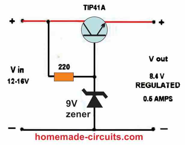
I would be glad to help you.
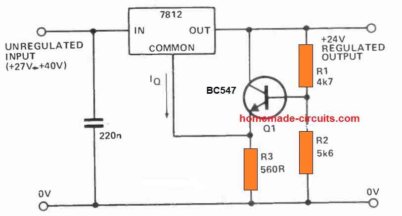
Did you consider using a transistor emitter follower configuration for converting your 6.4V into a regulated 5 V output?
Here’s the diagram which you can try:
You can replace the zener diode with a 5.6V zener diode for getting approximately 5V at the emitter side of the transistor.
That is fantastic thank you. Could I ask what wattage the zener / resistor should be for safe handling of 2amp possibly more?
Thank you in advance.
Warren
Both, the zener and the resistor can be rated at 1 watt each. The transistor will require a heatsink for maintaining an optimal working temperature.
If you want to avoid the heatsink you can perhaps replace the transistor with a TIP3055 or a TIP35
Amazing, your help has made a huge difference.
Thank you
The pleasure is all mine!
Dear Swagatam.
I have built the circuit provided using the 220 resistor and ran into a problem. Under higher loads (1amp) the circuit drops to much voltage. As I am using a 5.6v zener I wonder if the 220 resistor is to high for my purpose? I have done some very basic calculations. Could you give them your professional eye please?
1w rated zener so max power is 1w/5.6v = 0.178amps
using 7.4 power pack resistor needs to handle the remaining 7.4-5.6 = 1.8v
So 1.8v/0.178a = 10ohms minimum without any margin of error / tolerances in components.
Thank you in advance.
Warren
Hi Warren,
I think the base resistor can be calculated using the following formula:
R = (Supply – 0.7) x hFE / Load current
= (5.6 – 0.7) 30 / 1 = 147 ohms
For the exact value of the resistance, the hFE of the transistor will need to be known accurately.
The zener diode calculation is much more complicated. It is provided in the following article
https://www.homemade-circuits.com/how-to-calculate-zener-diode-resistor/
Dear Swagatam.
Thank you very much for pointing me in the right direction. I think the drain is more from the rapid prototype board I am using rather than your excellent diagram and values. I will construct a soldered version and test again. Many thanks.
Warren
No problem Warren! Thank you for updating the info. I hope the problem is solved once you build the soldered version of the circuit. All the best to you.
I need some way of keeping power to my Internet router to 12v when the alternator on my boat is charging the battery bank at 14.6v.
Possibly using a zener? I have searched in vain for other solutions….any ideas? Thanks, Paul.
You can simply use a 7812 IC regulator to regulate the voltage to 12V DC.
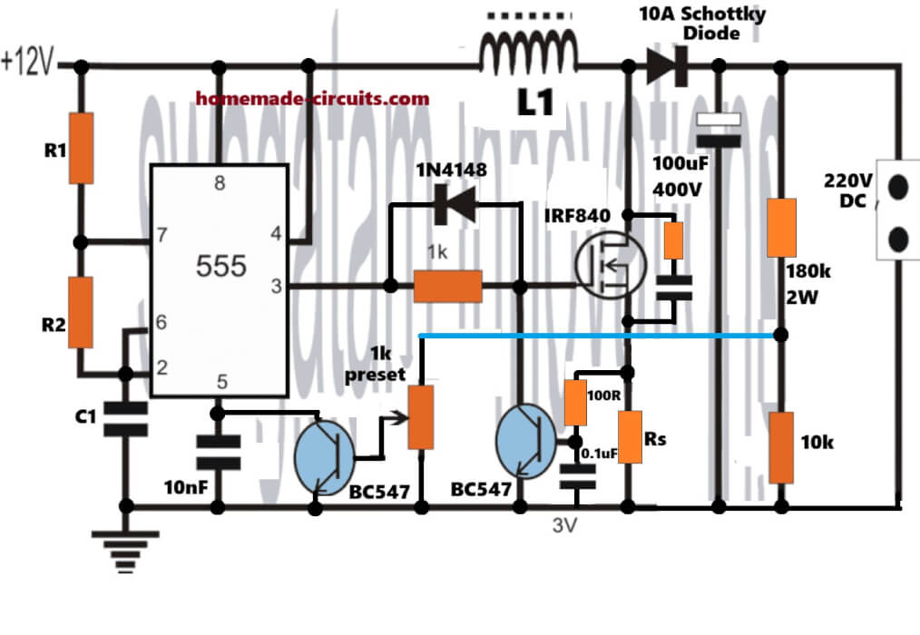
I’m having a hard time figuring out how to adjust the design you have. I need a DC-DC converter with a wide 40-60 volt input to a 12-14 volt 10A output. How I got my Amatuer Extra license I don’t know. I do not understand the math and the simulators have to many variables that I am getting no where. Do you have any suggestions?
The above circuits cannot be adjusted for 40 to 60V inputs. For 40 to 60 V you can probably try the following design:
https://www.homemade-circuits.com/lm317-variable-switch-mode-power-supply/
Hi Mr Swagatam;
On my SMPS circuit primer input side, after the rectifier bridge there are serial one resistor 220K and a capacitor (50V 100uF). The positive pole of this capacitor is also being fed by one leg of the transformer after a diode. And this capacitor is for the UC3548 PWM IC. The voltage here is about 17V. My question is the voltage as the 17V is OK or slighly higher for the IC?
And also could you please share your comment about that what kind of step down topology this is (300V DC to 17V DC)?
Hi Suat,
The max input supply voltage for UC3548 is 22V, so 17V looks fine to me…
If the SMPS has a transformer with primary/secondary winding then the topology is flyback converter topology…
hey sir can you tell me more about mp4560dn stepdown module !
Salman, all the details are given in the datasheet.
Please go through it. If you have any difficulty understanding it, let me know, i will try to solve it:
https://www.monolithicpower.com/en/documentview/productdocument/index/version/2/document_type/Datasheet/lang/en/sku/MP4560/document_id/305/
Do you have a dc-dc converter circuit with isolation without a transformer?
Isolation without a transformer looks impossible….sorry, currently I don’t have this type of circuit in this website…
I don’t know the details, but they have been around for some time now, and they use inductors (only 1 winding, not too many turns on it, and are made for a fast frequency oscillation made from the DC input) instead of the transformers.
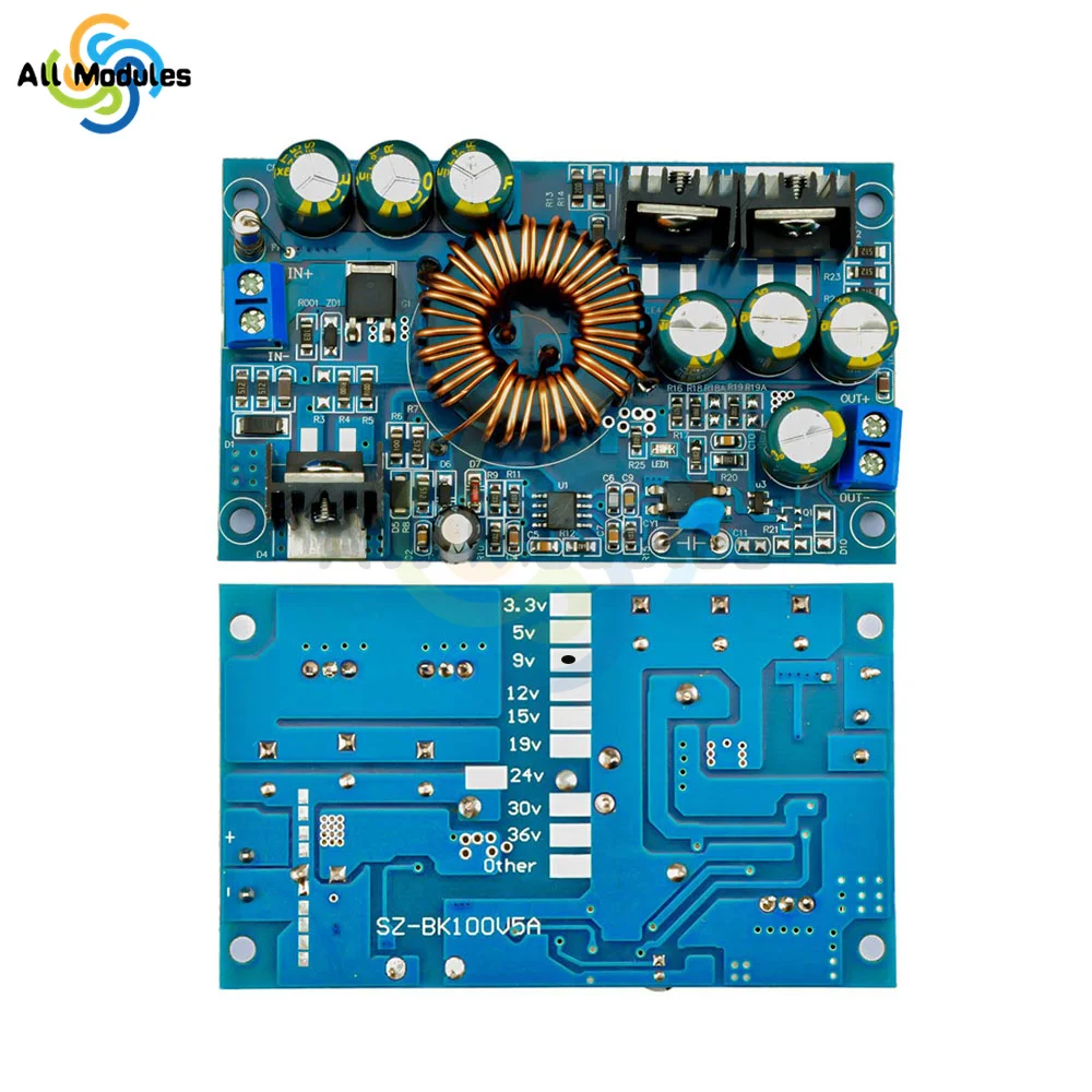
Example:
Will you investigate?
The ring inductor is the transformer which is providing all the isolation between the input and the output voltages..
I’m sorry I missed that. (The 2 windings looked indistinct.)
Do you have a circuit like it?
No problem, you can try the following example design, and calculate the transformer using this SMPS calculator:
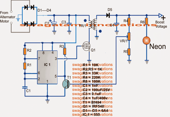
https://www.homemade-circuits.com/smps-transformer-calculator-2/
How should the component selection change based on input and output voltage and current? How do I know how much voltage and current to attempt and what it will do to efficiency and component damage? What is the voltage range(s) at which Bf494, IRF540 and 555 are best? What is “Boost Voltage?” (I don’t understand.) I assume the grounds on opposite parts of the circuit across the transformer have separate grounds, but doesn’t the connection between T1 and VR/1 mess up the isolation? How do I know the appropriate range for VR/1? What is “Neon?” (a load or indicator?)
If you can tell me the full specifications of the converter required by you, then I can customize the design according to your needs.
The exact voltage and current don’t matter too much, as I can use any fixed, adjustable, or unregulated voltages up to 40V, but I want to know the voltages, it needs to have good efficiency, low cost per watt, and a low number of turns on the transformer.
You can use the buck, boost, SMPS, 555 astable calculators from the following link, to calculate any desired parameter for your converter:
https://www.homemade-circuits.com/online-calculators/
Regarding what I just sent you, a happy medium might be 24V to 24V 3A.
You want to convert 24V back to 24V?
What is the greatest voltage that can be converted without inefficient SiC transistors? (I’m interested in using the most efficient type of isolated power conversion.)
I don’t know about that, you will need to find it by checking datasheets.
Awesome article ty.
>“ As the current across the coil increases, the voltage across R1 decreases”
I think you meant *increases*.
> 10 F electrolytic cap?
You mean 1000 uF ?
Thank you, glad you liked the article.
Actually, it “decreases” with respect to ground, but increases with respect to the positive line, because the transistors are PNP..
“deceases” indicates getting more and more negative, causing T3 to conduct harder ON.
Yes, you can use a zener diode with an opto coupler, but using a preset is more customizable than zener diode alone..
I really don’t need to change the voltage while it’s running for my application. If needed to make a voltage source or if it would be more efficient, please make a diagram with a zener diode and opto-coupler. If not, please tell how to find R5 and VR/1.
Can you make a diagram / specify values?
You just have to remove the R4, VR1 and put a 24V zener 1W diode between the positive rail and R5, cathode of the zener diode going to the positive rail, and anode to the R5, then connect the optocoupler’s LED anode with the zener/R5 junction. R5 can be a 2.2k resistor.
Thanks!
If I put a heatsink on Q1, the input is 24V, and TR/1 is adequate, how much input current should I allow to prevent burning?
You will have to calculate TR/1 using the following calculator:
https://www.homemade-circuits.com/smps-flyback-boost-converter-calculator/
Input current is not important, it can have any value. It is the load current that matters cannot exceed the MOSFET Q1 rating, and the transformer wire rating.
Limiting input current with fixed voltage limits wattage (both in & out) and therefore output current.
For your low current application you can use your input current limiting method. I basically meant to say that input current is immaterial, it will have no impact on the circuit, unless and until the load specification is wrongly selected.
The calculator doesn’t take load current and doesn’t give input current (peak nor RMS).
Note: This calculator is focused on giving basic SMPS design values like inductor size, frequency, number of turns, and output voltage. It does not include full electrical stress analysis like input RMS current, switch peak current, or efficiency estimation. For that you can use simulation tools like LTspice or detailed datasheet formulas.
The open-circuit voltage doesn’t seem like a very practical overall design figure to me. I want to power loads that draw current.
Sure, you can draw your own version and send it to me…
I wanted something of the same type of power conversion transformer/core and approximate number of turns as the S0230b5723c7e401f98d6d9af240b5789F.jpg I indicated earlier, with similar ampacity (e.g. 3A or 5A), including the relatively high efficiency available for this technology, as well as the isolation [which you suggested a 4-pin optocoupler could help provide], but I don’t want all of the automatic features built-in and I don’t know how to design it myself, so I’m asking for your help. I don’t need it to buck and would like an equal or, if not equal, higher, output voltage than input voltage without straying too far from the input voltage when the input voltage is close to the fixed value, but I’m interested in controlling it with the 24V zener and, although I didn’t exactly mention it earlier, it would be best if it normally kept its voltage up near that [as we discussed] with the zener, but preferably without maintaining output voltage when the current would otherwise overload the transistor, and if it had a low quiescent current. The input voltage will be limited to the 24V [or another fixed value] except at high input current draw, when it would help to lower output voltage to prevent overload. Short windings of big-diameter wire on TR/1 will prevent overload of TR/1, as well as reducing ohmic losses.
In that case, you can try the following tool, and apply it with my earlier 555 flyback circuit:
https://www.homemade-circuits.com/smps-calculator-using-toroidal-ferrite-transformer/
Are those or something needed to shut down the oscillator when it is about to cause overcurrent? How do we set up the minimum overcurrent protection?
When you are already limiting the input current, then no such protections are required…
only an RC snubber is needed across Q1…
When current is flowing through the primary coil of TR/1 and Q1 shuts off, it appears Q1 will be subject to very high voltage.
That voltage will be absorbed on the secondary side by the filter capacitor and the load…
Q1 is shown on the primary side. (The primary and secondary sides of a transformer have different phases.)
The energy stored inside the primary winding is thrown into the secondary winding which is then stored inside the filter capacitor. That is how a flyback system works. Q1 gets no high voltage, it only gets the Vinput voltage across it, for which it is rated appropriately.
There is no Vinput. The energy stored inside the primary winding is suddenly thrown into Q1 when Q1 attempts to turn off.
Please read this article:
https://www.homemade-circuits.com/do-we-need-a-freewheeling-diode-across-the-inductor-in-boost-converter/
No, there is no conductive path from the primary winding through the secondary coil.
You are right, so you can add a calculated snubber network across the primary winding.
Add a snubber network across the primary.
How about putting a capacitor in series with the primary and connecting the combination to an h-bridge connected to vin & ground?
That would be an overkill, it is simply not required, the standard design is the best!
I prefer the cool and energy-efficient way.
There is no need for energy-wasting resistorized circuitry like snubbers if the transistors are turned on and off at the right times. Can you make up a design for that to input power into a 2-transformer application for me? (I don’t know how to turn 8 transistors on & off at the right times, just that it is possible but tricky without resistors/snubbers to do in a way that won’t burn anything and it doesn’t even require any heatsinks. I can detail my application a little more.)
Even I don’t know how to do that, that is why i prefer the standard design as explained in the above article.
You can’t figure a way to switch the transistors when their corresponding capacitors reach peak charge and current through their corresponding coils is ready to cross zero?
Can you draw your concept and let me see it, then maybe I can try figuring it out…
Thanks! I’ll do that.
Here:

Why did you use two H-bridges and transformers?
I wanted both loads to be powered from the current source Vin. I don’t know the voltage of Vin, but I thought we might be able to calculate it and maybe the current from the specification of the model of the components T1-T8. I forgot an inlet capacitor, but power draw will be steadied some by the 1/4-wave offset too. It would also be nice if a driver for Vin could have a wide-range input or overvoltage protection without giving up much peak efficiency at substantial power draw or having much quiescent current. If not, or there was an unexpected delay between the cycling of the transformer-primary & capacitor pair timings, all of the h-bridge on the fast side could be temporarily turned off instead of immediately making the next step. The normal switching timing for bringing up the voltage should be: 1st T1 & T2 on with nothing else, next T1, T2, T3, & T4 on with the rest off, next T3, T4, T5, & T6 on with the rest off, next T5, T6, T7, & T8 on with the rest off, next T1, T2, T7, & T8 on with the rest off, and after all of that, it should repeat, each step made when the corresponding coil current is about to cross zero and the corresponding capacitor is at peak voltage.
I am finding it difficult to mentally simulate the entire setup, so I am unable to clearly understand the switching behavior of the design. It would be better if you could try testing it in some simulation software.
That 1st step is not part of the repetitive cycle.
At the time of each step, a capacitor’s charge is at a peak and the current through it, its transformer, and its H-bridge is 0. At this time, the H-bridge can reverse polarity to increase the later charge, by transferring power. That is what the cycle timings are for.
Please tell, what kind of PWM are you looking for and with what timing?
Not exactly PWM unless it’s feeding an inlet capacitor [through an inlet, iron-core high-current inductor, which could have a diode to ground]: the steps need to shut off the primary exactly when the energy is in the capacitor and the secondary coil and not in the primary coil. The back-on part of the steps could be delayed based on feedback/preset(s), but that would make some output noise. We could add a T9 between C1 and T1 and a T10 between C2 and T3, to reduce the noise, by filling-in for the H-bridges when an H-bridge is off, for an even number of steps. T9 and T10 would then supply TR1 and TR2 with only power already in C1 and C2, for more stability / clean output.
Let’s call an inlet transistor T0, an iron-core inductor L1, and inlet diode D0, for any future reference.
This will require a microcontroller or an Arduino operation, cannot be done with discrete components.
Can you write and specify what’s needed for RP2040 or RP2350 (generic versions of the Pico and Pico 2) microcontrollers? (I have an Uno, but I think it would be too slow.)
Can 1 or 2 0-6V 16-way MUX modules handle the task with 5-6 microcontroller pins (4 pins for a 4-bit address, and the pin(s) for input and output) while the microcontroller is also doing other things (e.g. running my 3D printer and/or more instances of my design)?
Can the microcontroller sleep when my loads are off / while voltage of stored energy remains adequate, or until a voltage or current could be about to be excessive (e.g. based on the fixed maximum possible increase over the latest value or last peak, perhaps via zener diode, capacitor with filter, optocoupler, etc. – discrete components)? (The sleep is intended to reduce quiescent power consumption. The voltage or current fixed at Vin by modulating T0, as we discussed earlier, by discrete components with regular PWM (or with PFM), fixes or limits some aspects/properties of everything downstream in the circuit and thereby allows the microcontroller to be able to sleep if coded and wired for it.)
That looks difficult, because I can only create basic Arduino codes not complex ones like this…
If it’s just a matter of getting the value from a mathematical formula you have into a variable, then, regardless of how complicated it is, if you send/post the formula, which other variables have which inputs, and which language, I can readily make a try at a statement, which try we could debug together in case it had error(s).
There are plenty of online free softwares which you can try…
Any spyware-free ones for Android?
Sorry, I have no idea about that.
You can add all the applicable protections explained in the following article, for Q1:
https://www.homemade-circuits.com/mosfet-protection-basics-explained-is/