In this article I will explain how we can build an Arduino-controlled H-Bridge sine wave inverter circuit using some easy parts. So this thing will basically convert DC into AC but in a way that looks like a sine wave, right? We are using an Arduino to generate PWM signals and these signals will drive an H-Bridge circuit made using IR2110 MOSFET driver ICs and power MOSFETs. This setup will allow us to switch MOSFETs in a controlled manner and create an AC output from our DC supply.
Understanding the Circuit Design
If you don't want to read the whole explanation, you can watch this video instead:
Now let us see the circuit diagram below and learn how this thing is actually working. We see the following main parts in the circuit:
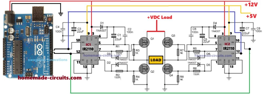
Note: Please make sure to replace all the 1N4007 diode with a UF4007 or any other fast diode like FR107 or BA159
Arduino Board – This is our brain. It gives out SPWM pulses that decide how our circuit will run.
IR2110 MOSFET Driver ICs (IC1 and IC2) – These devices take the standard SPWM signals from Arduino and make them compatible to switch the 4 N-channel H-bridge MOSFETs properly, using bootstrapping method.
MOSFETs (Q1, Q2, Q3, Q4) – These are the power switches. They turn the DC power ON and OFF in a specific way to create AC at the output.
Diodes (1N4007) and capacitors – These are for enabling the correct working of the bootstrapping network of the ICs for perfect switching of the 4 MOSFETs.
Other Capacitors and Resistors – These are small but very important because they keep everything running smoothly.
Power Supply – We need +12V and +5V for Arduino and the IR2110 ICs, and a high DC voltage for the MOSFETs, as per the load specifications.
What is Happening in the Circuit?
Now let us see how this works step by step:
Arduino generates SPWM signals at two output pins (Pin 8 and Pin 9). These signals keep changing width to create a shape equivalent to a AC sine wave.
IR2110 ICs receive these PWM signals and use them to switch the MOSFETs ON and OFF in a very specific way.
The H-Bridge made using four MOSFETs converts the DC bus supply into AC-like output by switching the current direction through the load using the SPWM switching.
At the output we get a sine wave approximation which means it looks like a sine wave but is actually made of fast-switching pulses.
If we add a filter circuit at the output then we can smooth these pulses and get a more perfect sine wave.
UPDATE: Get this Improved Arduino SPWM Code
Our Arduino Code for Sine Wave PWM
So now let us see the code. This is what the Arduino will run to generate the SPWM signals.
// By Swagatam
void setup() {
    pinMode(8, OUTPUT);
    pinMode(9, OUTPUT);
}

void loop() {
    // First half of the sine wave
    digitalWrite(8, HIGH);
    delayMicroseconds(500);
    digitalWrite(8, LOW);
    delayMicroseconds(500);

    digitalWrite(8, HIGH);
    delayMicroseconds(750);
    digitalWrite(8, LOW);
    delayMicroseconds(500);

    digitalWrite(8, HIGH);
    delayMicroseconds(1250);
    digitalWrite(8, LOW);
    delayMicroseconds(500);

    digitalWrite(8, HIGH);
    delayMicroseconds(2000);
    digitalWrite(8, LOW);
    delayMicroseconds(500);

    digitalWrite(8, HIGH);
    delayMicroseconds(1250);
    digitalWrite(8, LOW);
    delayMicroseconds(500);

    digitalWrite(8, HIGH);
    delayMicroseconds(750);
    digitalWrite(8, LOW);
    delayMicroseconds(500);

    digitalWrite(8, HIGH);
    delayMicroseconds(500);
    digitalWrite(8, LOW);

    // Second half of the sine wave
    digitalWrite(9, HIGH);
    delayMicroseconds(500);
    digitalWrite(9, LOW);
    delayMicroseconds(500);

    digitalWrite(9, HIGH);
    delayMicroseconds(750);
    digitalWrite(9, LOW);
    delayMicroseconds(500);

    digitalWrite(9, HIGH);
    delayMicroseconds(1250);
    digitalWrite(9, LOW);
    delayMicroseconds(500);

    digitalWrite(9, HIGH);
    delayMicroseconds(2000);
    digitalWrite(9, LOW);
    delayMicroseconds(500);

    digitalWrite(9, HIGH);
    delayMicroseconds(1250);
    digitalWrite(9, LOW);
    delayMicroseconds(500);

    digitalWrite(9, HIGH);
    delayMicroseconds(750);
    digitalWrite(9, LOW);
    delayMicroseconds(500);

    digitalWrite(9, HIGH);
    delayMicroseconds(500);
    digitalWrite(9, LOW);
}
What is Going On in This Code?
First we set up two output pins (Pin 8 and Pin 9). These will send out our PWM signals.
Then in the loop we turn the pin ON and OFF in a special pattern.
We start with narrow pulses and gradually increase the pulse width and then we reduce it back down. This creates a stepped sine wave PWM pattern.
After the first half cycle is done then we repeat the same thing on the other pin (Pin 9) for the next cycle.
This way our H-Bridge switches the MOSFETs in a proper sinusoidal wave like fashion.
What is Good about this Design
The design is actually very simple. We are using just an Arduino and some common components.
We do not need a sine wave generator here, right. The Arduino itself is making the sine shape using SPWM.
The H-Bridge works efficiently using the IR2110 ICs to make sure the MOSFETs switch correctly without overheating.
We can fine tune the SPWM easily, in case we want a different sine wave frequency, then we just modify the code a little.
How We Should Handle the Arduino Booting Delay
Now one very important thing that we must understand is that Arduino takes some time to start after we switch ON the power.
This happens because when we power ON the Arduino then it first runs its internal bootloader which takes a few seconds.
So during this time the IR2110 gate driver ICs and MOSFETs may not receive any proper signals from Arduino.
If that happens then the MOSFETs may turn ON randomly which can damage the ICs instantly, or cause a short circuit or explosion.
In order to make sure that the above booting delay does not burn the ICs and the MOSFETs during the initial power ON, we need to modify the above code as shown below:
// By Swagatam - Full Bridge Sine Wave Inverter Code with Delay

void setup() {
    pinMode(8, OUTPUT);
    pinMode(9, OUTPUT);

    delay(3000); // Booting delay (wait for 3 seconds before starting)
}

void loop() {
    // First pin (8) switching pattern
    digitalWrite(8, HIGH);
    delayMicroseconds(500);
    digitalWrite(8, LOW);
    delayMicroseconds(500);
    digitalWrite(8, HIGH);
    delayMicroseconds(750);
    digitalWrite(8, LOW);
    delayMicroseconds(500);
    digitalWrite(8, HIGH);
    delayMicroseconds(1250);
    digitalWrite(8, LOW);
    delayMicroseconds(500);
    digitalWrite(8, HIGH);
    delayMicroseconds(2000);
    digitalWrite(8, LOW);
    delayMicroseconds(500);
    digitalWrite(8, HIGH);
    delayMicroseconds(1250);
    digitalWrite(8, LOW);
    delayMicroseconds(500);
    digitalWrite(8, HIGH);
    delayMicroseconds(750);
    digitalWrite(8, LOW);
    delayMicroseconds(500);
    digitalWrite(8, HIGH);
    delayMicroseconds(500);
    digitalWrite(8, LOW);

    // Second pin (9) switching pattern
    digitalWrite(9, HIGH);
    delayMicroseconds(500);
    digitalWrite(9, LOW);
    delayMicroseconds(500);
    digitalWrite(9, HIGH);
    delayMicroseconds(750);
    digitalWrite(9, LOW);
    delayMicroseconds(500);
    digitalWrite(9, HIGH);
    delayMicroseconds(1250);
    digitalWrite(9, LOW);
    delayMicroseconds(500);
    digitalWrite(9, HIGH);
    delayMicroseconds(2000);
    digitalWrite(9, LOW);
    delayMicroseconds(500);
    digitalWrite(9, HIGH);
    delayMicroseconds(1250);
    digitalWrite(9, LOW);
    delayMicroseconds(500);
    digitalWrite(9, HIGH);
    delayMicroseconds(750);
    digitalWrite(9, LOW);
    delayMicroseconds(500);
    digitalWrite(9, HIGH);
    delayMicroseconds(500);
    digitalWrite(9, LOW);
}
Parts list
| Part | Specification | Quantity |
|---|---|---|
| Arduino Board | Arduino Uno (or any compatible board) | 1 |
| MOSFET Driver IC | IR2110 High & Low Side Driver | 2 |
| MOSFETs | IRF3205 (or similar N-channel) | 4 |
| Diodes | 1N4007 (for bootstrap & protection) | 4 |
| Resistors | 1KΩ 1/4W (MOSFET gate pull-down) | 4 |
| Resistors | 150Ω 1/4W (MOSFET gate series resistor) | 4 |
| Capacitors | 100nF (bootstrap capacitor) | 2 |
| Capacitors | 22uF 25V (power supply filter) | 2 |
| Load | Any resistive or inductive load | 1 |
| Power Supply | +12V DC (for MOSFETs) & +5V DC (for Arduino) | 1 |
| Wires & Connectors | Suitable for circuit connections | As needed |
Construction Tips
Now when we actually build this thing we have to be very careful about a few important things. Otherwise it may not work or worse, something may burn out right? So here are some super important construction tips that we must follow:
How We Should Arrange the Parts on the Board
If we use a breadboard then this circuit may not work well because high-power MOSFETs and drivers need strong, solid connections.
So we should use a PCB (Printed Circuit Board) or at least a perf board and solder the parts properly.
If we make a PCB then we must keep the MOSFETs and IR2110 ICs close together so that signals do not become weak or delayed.
The thick wires should go for high current paths like from the power supply to the MOSFETs and from the MOSFETs to the load.
The thin wires can be used only for signal connections like from Arduino to the IR2110 ICs.
How We Should Place the MOSFETs
The four MOSFETs should be placed in a proper H-Bridge shape so that the wiring does not become messy.
Each MOSFET should have short and thick connections to the IR2110 IC.
If we place the MOSFETs too far from the IR2110 then the signals may become weak and the MOSFETs may not switch properly.
If that happens then the MOSFETs can get hot and even burn out.
How We Should Fix the Heat Issue
If we use high current IRF3205 MOSFETs or similar ones, then they will heat up if we do not give them a heatsink.
So we must fix a big aluminum heatsink to the MOSFETs to keep them cool.
If we are making a high-power inverter (more than 1000 W) then we should also attach a cooling fan on the heatsink.
If the MOSFETs get too hot to touch then it means there is some issue and we need to check the circuit again.
How We Should Power the Circuit
The Arduino part runs on 5V and the MOSFETs need 12V or more to work.
So we must never connect 12V to Arduino, or it will burn instantly!
The IR2110 ICs need two power supplies:
12V for the high-side MOSFETs
5V for the logic section
If we mix up these power lines then the circuit will not work properly and the MOSFETs will not switch correctly.
How We Should Connect the Wires
The ground (GND) connection is super important. If the ground wiring is weak or long, then the circuit may behave weirdly.
We should use a common ground for all parts, meaning the Arduino ground, IR2110 ground and MOSFET source ground must be connected together.
If we see the circuit behaving strangely (like the output flickering or MOSFETs getting warm without a load), then we should check the ground connections first.
How We Should Check the Circuit Before Powering It Up
Before we switch ON the power we must double-check all connections to see if everything is correct.
If we have a multimeter then we should use it to check the voltages at different points before inserting the MOSFETs.
We will strictly need an oscilloscope so that we can check the SPWM signals coming from Arduino to see if they look correct.
How We Should Test the Circuit Carefully
The best way to test this circuit safely is by starting with a low voltage.
Instead of 12V we can first try with 6V or 9V to see if the MOSFETs are switching correctly.
If the circuit works well at low voltage then we can slowly increase to 12V and finally to the full voltage.
If we suddenly apply full voltage and something is wrong then something may burn out instantly!
So we must test step by step and keep checking for overheating or wrong behavior.
How We Can Add a Filter for a Smoother Output
This circuit makes an AC output using PWM but it is still made of fast pulses.
If we want a clean sine wave then we must add an LC filter at the output.
This LC filter is just a big inductor and a capacitor connected to the output.
The inductor removes the fast switching pulses and the capacitor smooths out the waveform.
If we do this properly then we can get a pure sine wave that is safe for appliances.
How We Should Protect the Circuit from Damage
We should always add a fuse in series with the power supply.
If something shorts or a MOSFET fails then the fuse will break first and save the circuit from burning.
If the MOSFETs fail then sometimes they fail shorted (meaning they always stay ON).
If that happens then huge current can flow and damage the transformer or other parts.
So it is always good to check the MOSFETs using a multimeter before applying high power.
Conclusion
So here we saw how we can make a sine wave inverter using just Arduino and an H-Bridge MOSFET circuit. We used IR2110 MOSFET drivers to properly switch the MOSFETs and PWM control from Arduino to generate our sine-modulated AC.
Now one thing to remember is that this output is still made of fast-switching pulses so if we need a pure sine wave then we must add a LC filter at the output to smooth it out.
But overall this is a very practical and easy way to make a sine wave inverter at home!


Questions & Answers
This circuit comes in handy since I have a 220vac toroidal transformer at 12 x 8A with no center tap. Then I would like to assemble it. But as I am not with arduino, I want to know if you can replace the arduino by another circuit? Thank you very much.
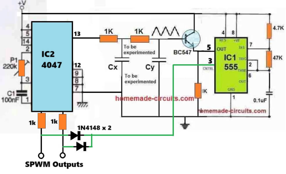
Sure, you can just remove the Arduino and replace it with any standard astable oscillator such as using IC 4047, or a BJT astable, or an 555, opamp, CMOS IC based astable oscillator etc….but in that case the output will be a square wave AC output….
Thank you very much for your quick reply , yes I understand but I meant that the circuit is the same in all aspects but without arduino ….
Sure, no problem! To get a reasonably ok sine wave output without using Arduino, you can replace the Arduino with the following circuit:
how do you calculate the L and C values for the circuit? for the lc filter
Just add a 3uF/400V capacitor at the output AC side of the H-bridge, that’s all is needed for smoothing the output AC into an almost pure sine wave.
Hello, I’m Jun Balista from the Philippines.
How come you did not mention the load voltage output anywhere in your article? It’s not even shown in your circuit diagrams. And the DC supply to the H-bridge was omitted, too! You should include both of them in the your next update perhaps? I believe those are very important things that you missed, sir.
Thanks.
Balista, I did not miss them, I did not mention them because they are not fixed values, and depends on the user application needs.
The LOAD voltage output will depend on the +VDC across the MOSFET drains, which can be any desired value depending on the load specifications.
The delay in the program does not mean anything because the program is executed after the bootloader. It is better to put some pullup or pulldown resistors. It’s even better to tie the SD pin to a pullup resistor, and later at the beginning of the program pull it down with arduino.
Hello brother wanna make solar inverter which get 300vdc directly from panels and convert it to 220vac 50hz sine wave but without transformer load is approximately 2000watt i have igbts 25n120,25t120,60t65,40t65 which one should i use and how to modify this circuit to achieve desired results i also have uno nano laying arround kindly help me
Hi Happie, yes you have opted for the right circuit design for your application. For 2000 watt at 220V, the current will need to be around 2000/220 = 9 amps, so you can actually use any of those mentioned IGBTs, but I would recommend 40t65 since it seems to be closest in terms of voltage and current to your application specifications…
Thanks sir..😊
definately I’ll change mosfets with igbt 40t60..
but having some question in my mind will this works with induction load like motors fans?
or do i need to add LC filter at the output to get modified sinewave ?
How much load can i use with this inverter maximum? if used 40t60 igbts
You are welcome Happie!
You can use any and all types of AC loads with the above inverter circuit.
Yes, an LC filter will be required to convert the SPWM into an pure sine waveform, so the output will be a pure sinewave not a modified sinewave.
The IGBT seems to be rated at 600V, 40 amps, so technically you can use any load rated at below 600V and current below 40 amps, and multiply the two parameters to get the maximum load that you can use.
Hey I’m here again with new request..
i don’t wanna use gate driver ic’s instead I’m gonna use optocupler to drive totem pole of bd139-140 for low side this totem pole okey but for high side 2 igbts+totem pole do i also need bootstrap circuit?
if yes can you guide me or can you give any diagram for reference 😊
Happie, totem pole can be used only at the low side of an H-bridge, i am not sure how it can be used at the high side because of the bootstrapping network which can be hooked up only with the high impedance gates of an IGBT or MOSFET.
If you know how to configure totem pole with High side of the driver then please let me know…
By the way, the half bridge drivers already have totem pole inside the chip built in…
NPN Transistor:
Collector → Gate of IGBT
Emitter → GND.
Base → Connected to the PNP transistor base
PNP Transistor:
Collector → Gate of IGBT.
Emitter → Vcc
Base → Connected to the NPN transistor base
after making this totem pole I’ll use bootstrap circuit..
from vcc I’ll add diode which is connected on the + side of capacitor and capacitor – on high side igbt’s source ..
the + side of capacitor will be connected on totem pole’s pnp transistor emitter to provide charged voltage to totem pole..
i hope you’ll understand I just trying it i don’t know it’ll work or not that’s why I’m here to get your help is this setup correct? kindly help me 😊
I am finding it difficult to interpret it in my mind, it is better to show it in schematic format.
However, please try it only if you are 100% sure that it will work, otherwise don’t try it…
But don’t worry I am working on it and will write an article soon on this topic…
i don’t wanna use driver ic’s bcz i found most of the ic’s are fake or not work properly…
😊
OK, no problem…
yep why make fake chips, to make things difficult.
you boys are on to something, have to find the right recipe. opti idolators have to be it for high wattage. have not tried it. there is a igbt driver board, tiring to fined the right one.
No need for any external driver boards, the IR2110 itself is able to provide up to 2 amps for driving the output devices, that means you can create all types of extremely high power inverters with the above configuration.
hello i used g50t65d these are beasts, but have not figure out the gate voltage to put them fully on. one things is for sure i have not blown one up like the mosfets, i don’t mine when they explode but when they catch fire, that’s when i freak out !!!!
You can use 15V as the gate supply for most of the IGBTs.
Just make sure to add snubbers for MOSFETs and also for IGBTs, to make them 100% fail proof:
https://www.homemade-circuits.com/explained-snubber-circuit-for-mosfet-h-bridge/
Hello brother
The battery size is 12 volts. What is the appropriate current? 9?
Yes brother, You can use 12V battery for the above sine wave inverter circuit, the Ah or the current capacity of the battery will depend on the maximum power of the load…
Hi. I get a square voltage waveform. What should I do to make a sine wave from this? I used a 3.3uf capacitor but it doesn’t change much. I know that an LC filter is needed but I don’t know what values to choose.
Hi, the above circuit should give a good sine wave output waveform. Please show me the waveform image, I will try to sort it out…
It’s not possible to send here photo of my oscilloscope. Please send me your e-mail. I’m using IRF3205 and the rest of components is exactly the same as yours.
Sure, you can send it to my email ID.
homemadecircuits
@gmail.com
Please send the waveform of the Arduino output also…
Sorry, Its of course 5V peak, my probe was not set correctly. But the shape is the same.
You should get the same waveform across the MOSFET output also, otherwise something may be wrong with the IR2110 circuit.
You sent me the following two images. The first one is the correct SPWM waveform which you are supposed to get across the MOSFETs also.
And why is the SPPWM waveform showing in mV? If it is from Arduino it should be 5V peak.
greetings to you sir, please can you help me with a push pull configuration of this circuit using two ir2110 MOSFETs driver. since I want to use a center tap transformer.
Enwongho, for a center tap transformer IR2110 is not required, you can use the following configuration instead:
https://www.homemade-circuits.com/arduino-h-bridge-sine-wave-inverter-circuit/
Goodday mr. Swagatam
i work on this inverter circuit today according to instruction, it work but i have some challenge with the frequency and output voltage
ON VOLTAGE AND FREQUENCY
-on 12v system output voltage was 255vac /49.9hz, no load,
when connected load, voltage drop to 156vac and frequency over-shoot to 5.4khz
– on 24v system output voltage was 330vac /4.5khz, no load,
when connected load, voltage drop to303vac and frequency over-shoot to 2.4khz
pls is there any way to control the output voltage with potentiometer and
stabilized the frequency
Hi Samuel, the frequency can never change because it is controlled by an Arduino, what you are seeing could be a false interpretation by your meter. You must use an oscilloscope if you want to verify the actual results.
The voltage drop is happening because your transformer is not correctly rated.
To get the exact transformer, check the average voltage between the two outputs of the Arduino, without connecting anything across these two outputs, except a voltmeter. This average voltage will give you the exact value of your transformer primary voltage rating. Next, make sure the power rating of your transformer is always higher than the load wattage, or vice versa. Transformer wattage = primary V * primary I. Here, primary refers to the low voltage DC side of the transformer.
For the feedback, you can try implementing the procedures explained in the following article:
https://www.homemade-circuits.com/making-an-egs002-equivalent-board-using-arduino/
ok engr, Swagatam
from output of my ardunio am getting
GND TO ardunio out A = 1.721VDC
GND TO ardunio out B =1.721VDC
out A & B = 4.02 VAC
FREQUENCY = 49.5HZ
according to what u said
“To get the exact transformer, check the average voltage between the two outputs of the Arduino, without connecting anything across these two outputs, except a voltmeter. ”
deos that mean this code meant for 12v system alone,
pls sir if there is loop to adjust in the code to work with 24v system kindly put me through
thanks
Samuel, I am not sure why you are seeing the voltage across ground as 1.72, and across the two outputs as 4.02V, because while one output is generating the PWM, the other Arduino output is supposed to be at ground potential, so in that case here also you should have got 1.721, or alternatively, you should have seen 4.02 across the common ground line also…
Anyhow, 1.72V is not making sense and seems incorrect. 4.02 V looks somewhat OK, but actually, since the Arduino is using 5V, the output average voltage should be equal to the RMS value of 5V…which is 5 / 1.41 = 3.54…this can be used with any transformer, whether 12V or 24V, that does not matter. Actually, to get the transformer primary value, you can simply use the same trick, divide battery voltage with 1.41…that’s all. So for 12V battery, the transformer primary can be 8.5V, for 24V it should be around 17V. Please use the code given in the following calculator and check the results:
https://www.homemade-circuits.com/sine-table-calculator-for-spwm-arduino-code/
….I think 1.72 is correct, because that’s the value of a single half cycle, so for a full cycle 1.72 + 1.72 = 3.44V, which looks close to 3.54V RMS value of 5V..
Jut divide you battery voltage with 1.41, and that would give you the approximate value of the transformer primary…
pls mr. Swagatam
base on this LC filter, is the series of capacitor and inductor will be connected to output of transformer or output of MOSFET stage .??????
(How We Can Add a Filter for a Smoother Output
This circuit makes an AC output using PWM but it is still made of fast pulses.
If we want a clean sine wave then we must add an LC filter at the output.
This LC filter is just a big inductor and a capacitor connected to the output.
The inductor removes the fast switching pulses and the capacitor smooths out the waveform.
If we do this properly then we can get a pure sine wave that is safe for appliances.)
Hi Samuel,
Yes, using an LC filter at the output of the inverter will certainly make the SPWM cleaner and almost identical to the mains 220V AC sine waveform. You can use the following calculator, to design your LC filter:
https://www.homemade-circuits.com/inverter-lc-filter-calculator/
hey how should we power the circuit ?? can i power directly with 12v dc battery??
Yes, you can use 12V battery directly to power the 12V supply of the ICs. For the 5V supply make sure to use 7805 IC with the 12V input from the battery.
Hey as i posted earlier how should i power the circuit i meant to say how do i power the dc input to convert in ac should i use 12v ??? directly or i have to use any other circuit before injecting the voltage in the drain of mosfet plz reply ?
Hi, If you want to use 12V-220V transformer at the “load” side then you can supply 12V DC from the battery to the drains of the MOSFETs. If you want to get 220V at the “load” side without a transformer, then you must use a 220V DC across the drains of the MOSFETs.
-heyy
25uf 25v cap is elctrolite and 100nf is ceramic right??
Yes, that’s correct…
wow great that you have this one all over the web, don’t tell no one but you are going to give the other people a run for your money. just looking at i know its great. i have three projects in the works because of your web site, thanks you are a god.
Thanks for your amazing words, glad you are finding the concepts helpful…please keep up the good work!
in the US we use 120 output. but the dc voltage is in my case is 260 volts. how dose it keep the the 120 at the output. yea as the battery’s run down it still keeps the 120 until it goes below 170 dc and at 145 it shuts down. it must be in the code of the the microconntroler. can you help with this, hope you under stand this.
You can simply do it by configuring a feedback network from the output AC of the inverter to the SD pins of the IR2110, through an opto-coupler. I will try to update the design soon…
Hi Swagatam. Thanks for sharing your project and making it available to everyone. I know very well the effort that goes into any type of project like this. I also love to do projects like this, and I’ve been thinking about making a 12 DC to 220 VA converter for a while. It’s been a while. At work, I’ve worked with circuits using the IR2110 and IRPF460 MOSFETs that can withstand up to 500 V. They worked with voltages of 340 V DC and everything went very well. The circuits worked very well because the consumption was constant. They lasted for years. But if there was any instability in the consumption, everything would explode. Please don’t take this the wrong way, these are just suggestions for your project. The Arduino is powered with 12 V. I think it would be with the yellow +5 V line. It occurs to me that to perhaps improve the project, a small 220/12V transformer could be used to output a sample that, once rectified, would then be fed to pin A0 of the Arduino. This would attempt to block the MOSFET gate voltage as quickly as possible. This would also provide a reference for increasing or decreasing the MOSFET pulse width based on the power consumption variation. Perhaps an optocoupler connected to the load output would be faster, acting very quickly on the MOSFET gates, blocking them, or on the IR2110s, which would then block the MOSFETs quickly. My experience is that if this isn’t done quickly, the MOSFETs will eventually blow. These are just a few ideas; I hope you don’t find this intrusive to your project. Thanks for everything, Swagatam.
Thank you very much Angel,
I appreciate your kind efforts to provide the useful safety suggestions for ensuring a long lasting sine wave inverter design.
I am sure the other readers will find the information very helpful…
Additional, please also consider putting snubbers across each of the MOSFETs:
https://www.homemade-circuits.com/explained-snubber-circuit-for-mosfet-h-bridge/
Thanks, Swagatam, installing snubbers could be a great solution. I’m currently quite busy with two projects I’m working on. I hope I can find a time to build your project; it’s sparked a lot of interest. Thank you so much for sharing your information. You have a very interesting blog. Best regards, and thank you.
You are most welcome Angel,
I am very glad that you liked the project and found it interesting.
Yes, snubbers can be really helpful in improving stability.
All the best with your projects, and let me know if you need any help later.
Hello Mr Swagatm Good day I am a great fan of your page and have been on many many of your projects in inverter design. Sir I build a 1kva 12v inverter with sg3525 and this Mos H drive but I got 9V spwm pure sign wave signal from sg3525 and ne555 and fed it to the ir2110 Mos H driver then the output from ir2110 driver is 7v which is connected as above circuit to the MOSFET 3205 but what am getting at the out put is 7vdc niit AC and it cannot drive the 12v- 220v AC transformer connected to the out out please what could be the issue
Thank you Samuel for your kind words, it is much appreciated!!
Yes, when an SPWM is used, it chops the 50 Hz frequency into narrow/wide sequencing blocks causing the average voltage of the pulses to drop, but the peak of these SPWM pulses remains always the same as the MOSFET drain voltage, which is 12V in your case.
To confirm this please check the output with an oscilloscope and check if the peak level is 12V.
Once you confirm this and also the SPWM waveform, then you must replace the 0-12V transformer with a 0-6V transformer and check the results further…
Hi, I saw your diagram. If I size the components, can it be used for 5kW? I look forward to hearing from you.
Best regards.
Yes, definitely, the inverter can be upgraded to any higher power level, by modifying the MOSFET/IGBTs accordingly and by adding suitably selected the snubber values…
https://www.homemade-circuits.com/rc-snubber-calculator-for-mosfets-relay-contacts-and-triacs/
How to know the switching frequency of the PWM from the code you used and how to increase it.
I’m trying to design an LC filter
Output voltage (rms) = 8.46
Output power = 10W
Output frequency = 50Hz
And I put 300Hz cut off frequency
I’m getting 3.8mH and 72uF which is large
If I increased the switching frequency to 20kHz
Then I can select a cut off frequency of 5000 so the filter will be smaller
If you add up the microseconds for each cycle, it gives 10ms, and for both cycles it is 20ms, so the frequency becomes 50Hz…
Sorry I meant the switching frequency of the triangle wave that’s being compared with a sine wave to produce the pwm waves
There’s no triangle wave comparison in Arduino, the SPWM is generated directly by the Arduino. If you want to change the number of blocks inside each SPWM waveformm, then you can use the following code concept instead…
https://www.homemade-circuits.com/sine-table-calculator-for-spwm-arduino-code/
Hi, thank you so much for your efforts.
There is something I don’t understand about the IR2110 IC. I saw that VIL is about 6V and VIH is about 9.5V, and I thought these values are not compatible with Arduino. So how did it work for you? I believe that VIL and VIH values correspond to the logic levels coming from the Arduino PWM output. Can you explain if I misunderstood something? Thanks in advance.
Hi, the 6V is used for the internal working of the IC, and the 9.5V or 12V supply to the IR2110 is meant for driving the MOSFETs, they do not interfere with the Arduino 5V
The job of Arduino is to feed the 5V logic signals to the IR2110 which then responds to these signals by switching the MOSFETs accordingly. The IR2110 HIN and LIN inputs are TTL compatible so they accept the 5V signals without any issues and drives the H bridge MOSFETs….
what if I wanna do it with esp32 (which is 3.3v pwm) can you give me some information?thanks in advance
Yes, you can use ESP32 directly because its 3.3V PWM is compatible with IR2110 logic input. Just make sure the ESP32 ground is common with the driver stage, while IR2110 keeps using the 12V supply for gate driving. ESP32 is actually better because it provides precise hardware PWM and dead-time control through MCPWM which makes sine-wave inverter operation more stable than Arduino.
THANKS SO MUCH SIR , FOR YOUR WELL FAVOUEBLE CONCERN ON CIRCUITHOME MADEINVENTION..
PLEASE, USING PROTUSE TO RUN THIS TEAST IS IT RECOMENDABELE.. WILL IT GIVE AN EFFICIENT TEST RUNNING CONFIRMATION BEFORE TRANSITIONING TO THE REAL HARDWARE ASSEMBLY.
Obinna, You can simulate the circuit on any suitable software to confirm the results…
hi sir
If I use an isolated DC-DC converter to supply the IR2110 through the VB and VS pins in order to eliminate the bootstrap circuit for very low-frequency operation, and if I use two IR2110 ICs for a full-bridge application, do I need two isolated DC-DC converters or is one sufficient to supply both IR2110 drivers?
Hi Ali, you will need two separate DC DC converters for the two high side MOSFETs of the two H bridge ICs…
Hi sir,
Sorry for the many questions, and thank you very much for your patience.
I noticed that during dead-time
(when both HIN and LIN are LOW), the VS node still shows a small fluctuating voltage.
This causes my load to receive a small voltage even though both MOSFETs are OFF.
Is this normal? If not, what could cause it and how can I fix it I searched the whole internet and couldnt find answer ?
Hi Ali,
That doesn’t look possible to me, because if all the MOSFETs are turned OFF, then the load cannot get any voltage. I think what you are seeing is parasitic voltage, and can be eliminated with a capacitor across the load terminals…
I hope you have connected the 1k resistors directly across the MOSFET gate/source terminals…
So now, please connect a capacitor across the load, having voltage rating higher than the max load voltage rating, and then check the response.
Hi, thanks for your suggestion.
The issue is that I already checked those points (gate pull-down resistors, wiring, and I also tried adding a capacitor across the load). However, I noticed something important: VS seems to remain floating, and as soon as I connect the diode between VB and VCC, I start measuring a small voltage appearing on VS.
This voltage looks like a parasitic/leakage voltage because it drops when the load resistance decreases, but I’m not 100% sure yet.
What confuses me is that I tested the circuit in a very simplified setup: I removed all MOSFETs, load wiring, and other components, and kept only the IR2110 with VB connected to VCC through a diode. Even in this case, I still see that VS itself is the source of that small voltage, not the MOSFETs and not any parasitic conduction through the power stage.
So my question is:
Is it normal for VS to float in idle mode?
And is it normal that VS can provide a very small voltage to the load (for example, I tested it with an LED and it still shows a small effect)?
Also, I’m using a Half-Bridge configuration (not a full bridge).
If this behavior is expected, what is the proper solution for sensitive loads where we need 0V at the output during IR2110 idle state, without any small residual/parasitic voltage coming from VS?
Yes this is normal. In IR2110, the VS is a floating node and will remain un-defined in idle when no MOSFET or load path is present. The small voltage you see is due to internal leakage and capacitive coupling inside the IC, not the real output power, just a high impedance effect.
To fix this, you can add a pull-down resistor (around 47k–100k) from VS to ground so that the node stays at 0V during idle and eliminates the residual voltage.
in the Application Note AN-978, there is a statement referring to parasitic voltages on the switching node. I will write the quote here
“2.3 High-Side Channel
This channel has been built into an “isolation tub” (Figure 3) capable of floating from 500 V or
1200 V to -5 V with respect to power ground (COM). The tub “floats” at the potential of VS.
Typically this pin is connected to the source of the high-side device, as shown in Figure 2 and
swings with it between the two rails”
Could you confirm if my understanding is correct .
My understanding is that VS is a floating node, and therefore in idle or dead-time conditions the output is not necessarily 0V. Instead, VS can show a small voltage (for example 2V, 10V, or 12V), depending on parasitic effects.
This voltage is not a real driven output from the IC, but rather caused by parasitic capacitances and leakage currents.
Also, when a load is connected, this voltage drops significantly, but it does not behave like a solid regulated output.
Is this interpretation correct?
Yes, that’s correct!
since the IR2110 already provides proper gate charging and discharging current for the MOSFETs, what is the actual purpose of placing a 1k resistor between the gate and source?
It is to ensure the MOSFET never remains floating even for a microsecond during the transitions, or under any any other circumstances…it provides the MOSFFET gate a guaranteed 0V, under no voltage condition at its gate.
Sir please I need help to generate a pwm inverter signal with a pic16f877a
Hi Julius,
I will try to update the code for you soon….please keep in touch…
Hello, sir Swagatam. I tried doing your circuit but it didn’t work when I tried it exactly on the proteus 9. I tried running the simulation, I used the AC voltmeter and no voltage. Also, I tried using the oscilloscope, but there is no sine wave.
Hello Umar, the above circuit has no problems…everything is correct in the concept, and it will work if you build it practically.
If your proteus is not working, please try to find out why the software is unable to simulate this correctly designed circuit…
I’m very sorry, sir. I tried it again and it actually work, but the problem is on the Proteus itself where the timestep has its limit, this is due because of my laptop cpu core is at 100%, so the simulation itself is not running in real-time and its delayed. Also, if I change the Load into LC filter and then use trafo will it work sir? Sir, sorry for asking too many I also want to know if you have a paper for this or any reference paper for this circuit. Thank you very much, sir.
Thank you Umar, I understand your problem, but I am not so sure about proteus results, since i have not used it for this circuit so far…if you are using a transformer, ten LC filter will not be required…you can connect the trafo primary directly in place of the load..
This circuit was designed by me so I don’t have any reference paper, but i can answer any question you have and solve all you doubts, if you have any…so you can feel free to ask them here…
Hello, sir swagatam. Thank you very much for your answer, right now I’m building the circuit. I was thinking using the LC filter to make the sine wave more smooth when check on oscilloscope. What do you think, will it work fine?
Also, before I test it I want to make sure, about the +VDC in the circuit. Is the Input just a positive VDC through both drain of the mosfet (Q1 and Q3)?
Thank you very much, sir swagatam.
No problem at all Umar, you can definitely try the circuit and let me know if you have any issues with the circuit.
Yes, +VDC is the DC load voltage which is applied only to the drains of the upper two high side MOSFETs, this voltage can be +220V DC, +300V DC, or +600V DC, whatever is applicable for the load.
But remember the ground line is common for all the 3 supply voltages, ground is common for +5, +12 and the +VDC MOSFET supply. Initially you can use +12V for the +VDC and use a transformer in place of the load, to confirm the working of the circuit.
Yes, an LC filter can be used for improved sine wave outcome. You can use the following calculator for dimensioning the LC filter:
https://www.homemade-circuits.com/inverter-lc-filter-calculator/
I’ve tried connecting all the components, which you can see here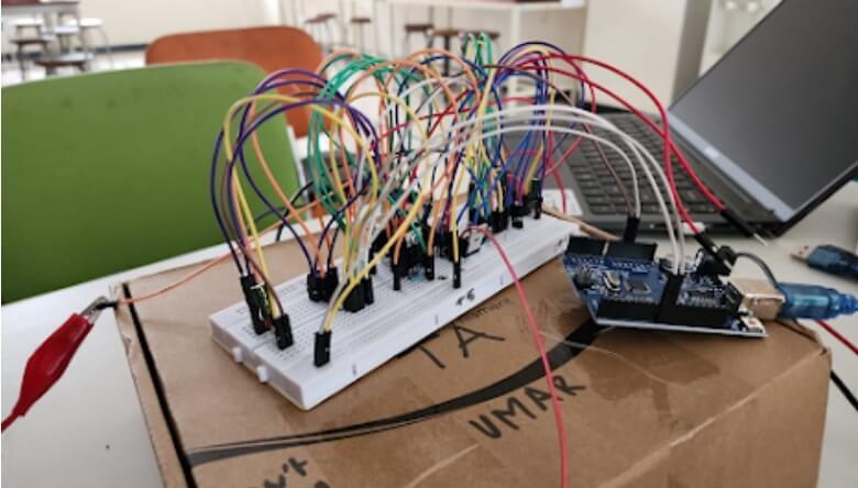
But, when I tried it, I used multimeter to check the voltage of the load output by putting a sliding variable/variable resistor as the load and parallel for the voltmeter, because right now I don’t have Trafo. I wanted to check just the voltage AC. I set for the VDC for 12 VDC, but the outcome is not 12 VAC. I turned it on just for a moment so it won’t fried the components. Do you have any idea what is wrong with the circuit? Thank you very much.
I think breadboard is not the right way to test this complex circuit.
You must build it on a perf-board by soldering the components, with IC sockets, and test the circuit step wise, not altogether.
First check the waveform from the Arduino output, and confirm it is correct SPWM. Then build only half bridge section of the IR2110, and check the waveform at the MOSFET output, and confirm it is same as the Arduino but only half cycle.
Next, build the other side of the H-bridge and do the same…
And finally integrate all the stages together, by soldering.
In this way you can complete the project successfully…
Thank you very much sir for the directions. I will try again and change it to perf-board. I would like to ask for the +12V, do you get it from the adaptor or power supply DC, if it is from the adaptor how do you do it? Because I used 2 powersupply DC for testing the circuit.
Also, I would like to ask if I can contact you with social media, so it is easy for us to discuss about this. Thank you very much for you help, sir.
Hi Umar, 12V DC from adapter is also a DC power supply, so it does not matter from which source it is. It just needs to be 12V DC.
So in the circuit you just need two DC supplies 5V and 12V. 5V and 12V for the IR2110, and the same 12V for the MOSFET drains, and also for the Arduino 12V supply pin.
I am not active on social media, but may be you can contact me on youtube, however I reply faster on my blog.:
https://www.youtube.com/watch?v=-eAjZef1C2w
Hello, sir Swagatam. I would like to thank you until now for helping and direction. I would like to ask for the HO and LO IC testing, you can check it on my blogger link: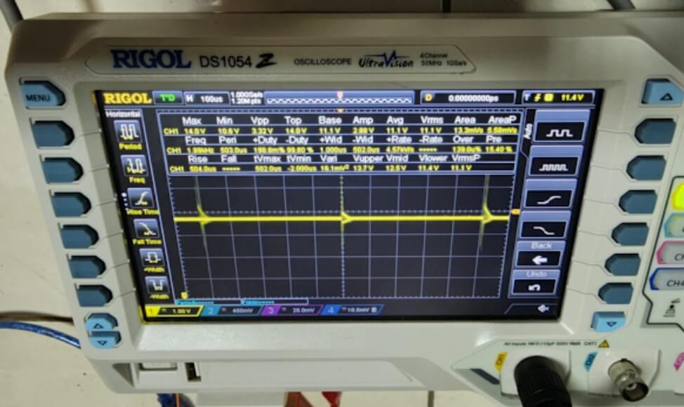
Thank you very much.
Hello Umar,
The LO pin can be measured directly with respect to ground.
But the HO pin is floating output, so it must be measured only with respect to VS, not the ground. Otherwise the waveform will appear incorrect.
But all these are not required, you can do the same by connecting the half bridge mosfets, and then check the waveform across the midpoint of the MOSFETs and ground or IC +12 supply.
Hello, sir Swagatam. I’m very sorry I gave out the wrong link, it should be this one:
umarfinalproject.blogspot.com/2026/04/final-project
Thank you very much.
Hello, sir Swagatam. I would like to ask about the trafo, I want the input from the +VDC Load is 24VDC and turn it into 24VAC. The output from the trafo is 150 Watt with a 220VAC 50Hz, the problem is I tried finding it on online and I couldn’t find it. Is there something I’m doing it wrong?
Hello Umar,
To get a 24V AC sine wave, you do not need a transformer in this circuit, you can get it directly across the H bridge MOSFETs, by applying around 24 * 1.41 = 34V DC at the +VDC.
pls I need your help, on egs002 module, can I drive a power MOSFET of 48v 5kva inverter direct with egs002 without external driver, or maybe because of the heavy power MOSFET I should put (tlp350) at the egs002 spwm output or a totem pole driver. pls give me a diagram to follow thank
Bright, you will need to employ a special arrangement such as this:
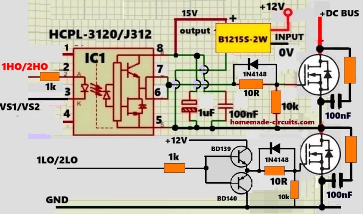
Hello, sir swagatam. It’s been a long time I haven’t contacted you, sorry for disturbing you. I would like to ask about the mosfet, what is the ideal way to connect to the circuit. I was thinking of doing it one by one, like placing the Q1 first and then check if it works. Then, the Q2, and then the rest. Or should I do it with Q1 and Q2 first, and check if it works and then the Q3 and Q4. I would like to know what do you think first or maybe you have some suggestion that works best. Thank you very much.
No problem Umar, and Thank you for your question…
Yes using Q1 and Q2 half bridge stage first is a good idea and then replace with the other half bridge, Q3, Q4.
Connect the load between the MOSFET source/drain junction and ground.
Before that, make sure to check the Arduino output waveform with an oscilloscope…
Thank you for your direction, sir swagatam. Yes, I have checked the output waveform from the arduino and also the output from the HO and the LO from the IC, and it shows the PWM waves. I would like to ask the again just to make sure. I have connected the Q1 and Q2 to the circuit. In order to test it correctly, I should turn on the arduino first, and then the +VDC load. Is this correct sir?
I would also like to ask several questions again. I want to check the VAC from ‘LOAD’, so if I put the positive probe on the ‘LOAD’ and the negative probe on ground from Oscilloscope. Is this the correct way to check the VAC?
I would also like to ask if I want to connect the +VDC Load from 24VDC Battery, what is something that I should be aware of, before it connect to the +VDC Load.
Thank you very much, sir swagatam.
You are welcome Umar,
yes…turn on the arduino first, and then the +VDC load.
yes…put the positive probe on the ‘LOAD’ (mosfet S/D junction) and the negative probe on ground from Oscilloscope, that’s the correct way to check the VAC?
Nothing to worry about connecting +24V DC for the +VDC, the half bridge IC will take care of the load and the mosfet switching correctly. For initial safety, you can connect a 24V bulb in series with the +VDC…
I would like to ask again, sir swagatam. My progress is I’ve already connected the mosfet Q1 and Q2 with the circuit. I also use 1 PSU DC and parallel it with IC Pin 3 and also at the +VDC Load, I set the PSU with 12VDC and 0.5 Ampere. I’ve also connected to the Oscilloscope and I did not get any result (no wave, just straight line). I would like directions for what I’ve been doing wrong. Thank you very much.
Umar, did you connect the HIN, LIN inputs with the Arduino? And +12, +5V DCs to the respective lines?
Pease check the waveform across HIN and LIN with respect to ground and check mosfet waveform across gate and source.