The common problem with many low cost inverters is their incapability of adjusting the output voltage with respect to the load conditions. With such inverters the output voltage tends to increase with lower loads and falls with increasing loads.
The circuit ideas explained here can be added to any ordinary inverter for compensating and regulating their varying output voltage conditions in response to varying loads.
Design#1: Automatic RMS Correction using PWM
The first circuit below can be considered perhaps an ideal approach of implementing a load independent auto output correction using PWM from a IC 555.
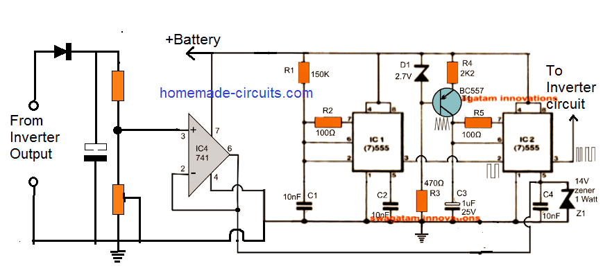
The circuit shown above can be effectively used as an automatic load triggered RMS converter and could be applied in any ordinary inverter for the intended purpose.
The IC 741 works like a voltage follower and acts like a buffer between the inverter output feedback voltage and the PWM controller circuit.
The resistors connected with pin#3of the IC 741 is configured like a voltage divider, which appropriately scales down the high AC output from the mains into a proportionately lower potential varying between 6 and 12V depending upon the output status of the inverter.
The two IC 555 circuit are configured to work like modulated PWM controller. The modulated input is applied at pin#5 of the IC2, which compares the signal with the triangle waves at its pin#6.
This results in the generation of the PWM output at its pin#3 which varies its duty cycle in response to the modulating signal at the pin#5 of the IC.
A rising potential at this pin#5 results in the generation wide PWMs or PWMs with higher duty cycles, and vice versa.
This implies that when the opamp 741 responds with a rising potential due to a rising output from the inverter causes the output of IC2 555 to widen its PWM pulses, while when the inverter output drops, the PWM proportionately narrows at pin#3 of IC2.
Configuring the PWM with Mosfets.
When the above auto correcting PWMs is integrated with the mosfet gates of any inverter will enable the inverter to control its RMS value automatically in response to the load conditions.
If the load exceeds the PWM the inverter output will tend to go low, causing the PWMs to widen which will in turn cause the mosfet to turn ON harder and drive the transformer with more current, thereby compensating the excess current draw from the load
Design#2: Using opamp and Transistor
The next idea discusses an op-amp version which can added with ordinary inverters for achieving an automatic output voltage regulation in response to varying loads or battery voltage.
If you don't want to read the following description, you can watch this video instead:
The idea is simple, as soon as the output voltage crosses a predetermined danger threshold, a corresponding circuit is triggered which in turn switches OFF the inverter power devices in a consistent manner thereby resulting a controlled output voltage within that particular threshold.
The drawback behind using a transistor could be the involved hysteresis issue which could make the switching fairly over a wider cross section resulting in a not so accurate voltage regulation.
Opamps on the other hand can be immensely accurate as these would switch the output regulation within a very narrow margin keeping the correction level tight and accurate.
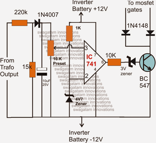
The simple inverter automatic load voltage correction circuit presented below could be effectively used for the proposed application and for regulating the output of an inverter within any desired limit.
The proposed inverter voltage correction circuit can be understood with the help of the following points:
A single opamp performs the function of a comparator and a voltage level detector.
Circuit Operation
The high voltage AC from the transformer output is stepped down using a potential divider network to about 14V.
This voltage becomes the operating voltage as well as the sensing voltage for the circuit.
The stepped down voltage using a potential divider corresponds proportionately in response to the varying voltage at the output.
Pin3 of the opamp is set to an equivalent DC voltage corresponding to the limit which needs to be controlled.
This is done by feeding the desired maximum limit voltage to the circuit and then adjusting 10k preset until the output just goes high and triggers the NPN transistor.
Once the above setting is done the circuit becomes ready to be integrated with the inverter for the intended corrections.
As can be see the collector of the NPN needs to be connected with the gates of the mosfets of the inverter which are responsible for powering the inverter transformer.
This integration ensures that whenever the output voltage tends to cross the set limit, the NPN triggers grounding the gates of the mosfets and thereby restricting any further rise in the voltage, the ON/OFF triggering continues infinitely as long as the output voltage hovers around the danger zone.
It must be noted that the NPN integration would be compatible only with N-channel mosfets, if the inverter carries P-channel mosfets, the circuit configuration would need a complete reversal of the transistor and the input pinouts of the opamp.
Also the circuit ground should be made common with the battery negative of the inverter.
Design#3: Introduction
This circuit was requested to me by one of my friends Mr.Sam, whose constant reminders prompted me to design this very useful concept for inverter applications.
The load independent/output corrected or output compensated inverter circuit explained here is quite on a concept level only and has not been practically tested by me, however the idea looks feasible because of its simple design.
Circuit Operation
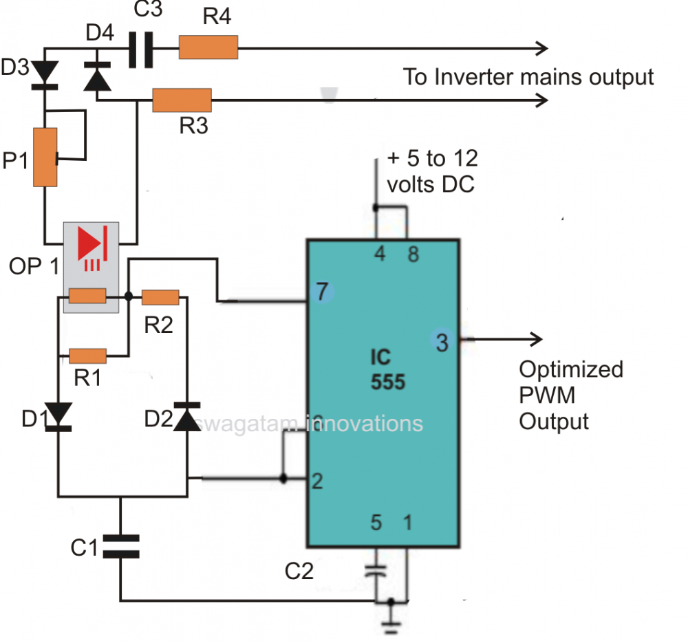
If we look at the figure we see that the entire design is basically a simple PWM generator circuit built around the IC 555.
We know that in this standard 555 PWM design, the PWM pulses can be optimized by changing the ratio of R1/R2.
This fact has been appropriately exploited here for the load voltage correction application of an inverter.
An opto-coupler made by sealing an LED/LDR arrangement has been used, where the LDR of the opto- becomes one of the resistors in the PWM "arm" of the circuit.
The LED of the opto coupler is illuminated through the voltage from the inverter output or the load connections.
The mains voltage is suitably dropped using C3 and the associated components for feeding the opto LED.
After integrating the circuit to an inverter, when the system is powered (with suitable load connected), the RMS value may be measured at the output and the preset P1 may be adjusted to make the output voltage just suitable enough for the load.
How to Set Up
This setting is probably all that would be needed.
Now suppose if the load is increased, the voltage will tend to fall at the output which in turn will make the opto LED intensity decrease.
The decrease in the intensity of the LED will prompt the IC to optimize its PWM pulses such that the RMS of the output voltage rises, making the voltage level also rise up to the required mark, this initiation will also affect the intensity of the LED which will now go bright and thus finally reach an automatically optimized level which will correctly balance the system load voltage conditions at the output.
Here the mark ratio is primarily intended for controlling the required parameter, therefore the opto should be placed appropriately either to the left or the right arm of the shown PWM control section of the IC.
The circuit can be tried with the inverter design shown in this 500 watt inverter circuit
Parts List
- R1 = 330K
- R2 = 100K
- R3, R4 = 100 Ohms
- D1, D2 = 1N4148,
- D3, D4 = 1N4007,
- P1 = 22K
- C1, C2 = 0.01uF
- C3 = 0.33uF/400V
- OptoCoupler = Homemade, by sealing an LED/LDR face to face inside a light proof container.
CAUTION: THE PROPOSED DESIGN IS NOT ISOLATED FROM INVERTER MAINS VOLTAGE, EXERCISE EXTREME CAUTION DURING THE TESTING AND SETTING UP PROCEDURES.



Questions & Answers
where can I send you the pictures
Please send it here through Google drive link, in shared mode…
hi sir the second circuit can decrease the output voltage if it exceed the threshold.but when the voltage gets reduced as a result of overload how can it be increased automatically by the circuit? thanks u sir
Hi Abubakar,
If an overload low voltage happens then the second circuit can be used to increase the PWM of an IC like sg3525 and correct the output voltage, however this can be possible only if we keep sufficient headroom for this adjustment and make sure the load is not exceeding the transformer and battery power thresholds…
Please I made this circuit but the LED wasn’t turning on to indicate that setting was successful on. I need your help. Please can I replace the 120k resistor with 100k resistor?
If your inverter output is 220V then the 220k resistor cannot be replaced with 100k.
Please measure the voltage across the 10uF, after applying 220V at the input side. It should be around 12V.
Put LED between opamp output pin and ground through a 1k resistor and check again.
How can I integrate that circuit with SG3524 inverter circuit as feedback system for voltage regulation
You just have to connect the anodes of the two diodes with the two gates of the SG3524 MOSFETs separately. One 1N4148 anode will connect with one MOSFET gate, and the other with the other MOSFET gate.
How can I integrate the AVR circuit with sg3524 PWM IC
Please explain the working you are trying to achieve, so that I can understand the purpose.
I have an inverter which uses IC SG3524
It’s voltage drops with certain loads so I wanted to add that circuit for regulating the output so that the output remains stable
Please specify how is the AVR output designed to operate regulate the inverter voltage?
Anyway if the inverter voltage is dropping due to overload, then no AVR circuit can solve it.
How can this Opamp method be used for a non center tap transformer (H-bridge)
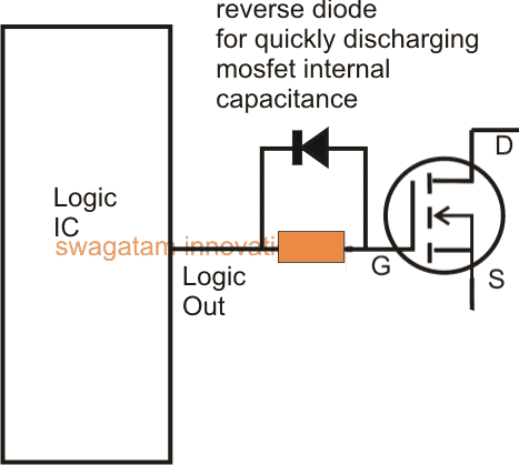
You just have to connect the diode anode ends with the gates of the two low side MOSFETs. Make sure to use a 1k resistor as the gate resistor for all the 4 MOSFETs, and connect reverse diodes across this gate resistor, as shown below:
Can we use the circuit above to regulate a diesel generator output voltage?
Yes, that is possible with this circuit…
good day sir I tried the circuit and it works fine..
I want to add an overload protection to the output side, please how do I go about it ?
which one
Sorry, I was referring to this circuit:
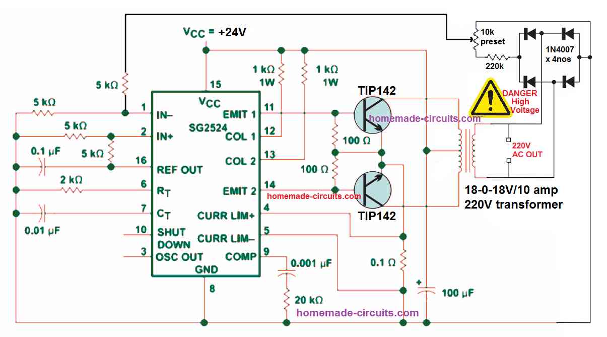
Which inverter circuit are you using?
Thank you Hillary,
The above circuits are designed to control overcurrent and overload both….
Dear swagatam,
Trust you good?.
My problem is still about the feedback control circuit. Please I need your help. Now, I have designed the arduino sine wave in your description and it is working perfectly. For the last time please where should I connect the output from the feedback control? Thanks in advance for your help.
Thanks for getting back to me. I will design it soon and when I’m done I will send you a full working picture and a video.
Sure, no problem, all the best to you!
Thank you Jonathan, glad you could build the inverter circuit.
The connection details of the feedback control circuit with the Arduino inverter is provided under the same Arduino inverter article. Please check it again, and let me know if you have any difficulty understanding it.
https://www.homemade-circuits.com/arduino-pure-sine-wave-inverter-circuit/
One more question. Please I have 5 mosfets at the low driver side. And if I’m to connect the cathode of the diode directly to the 5 mosfet gates, should I also connect the 50ohms to each of the gates or only one 50ohms to all the gates? Thank you
An H-bridge low side is supposed to have 2 mosfets only, why have you used 5 mosfets, and how are they configured? please let me know…
Swagatam please I said I did full bridge not half bridge. Thank you
H-bridge refers to full bridge….how can you have 5 low side MOSFETs in an h-bridge or a full bridge topology?