SSR or Solid state relays are high power electrical switches that work without involving mechanical contacts, instead they use solid state semiconductors like MOSFETs for switching an electrical load.
SSRs can be used for operating high power loads, through a small input trigger voltage with negligible current.
These devices can be used for operating high power AC loads as well as DC loads.
Solid State Relays are highly efficient compared to the electro-mechanical relays due to a few distinct features.
Main Features and Advantages of SSR
The main features and advantages of solid state relays or SSRs are:
- SSRs can be built easily using a minimum number ordinary electronic parts
- They work without any form of clicking sound due to the absence of mechanical contacts.
- Being solid state also means SSRs can switch at much faster speed than the traditional electro-mechanical types.
- SSRs do not depend external supply for switching ON, rather extract the supply from the load itself.
- They work using negligible current and therefore do not drain battery in battery operated systems. This also ensures negligible idle current for the device.
Basic SSR Working Concept using MOSFETs
In one of my earlier posts I explained how a MOSFET based bidirectional switch could be used for operating any desired electrical load, just like a standard mechanical switch , but with exceptional advantages.
The same MOSFET bidirectional switch concept could be applied for making an ideal SSR device.
For a Triac based SSR please refer to this post
Basic SSR Design
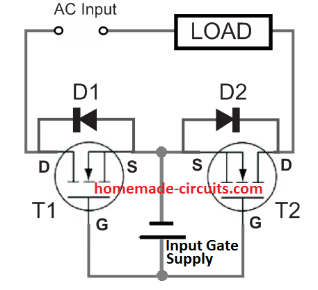
In the above shown basic SSR design, we can see a couple of appropriately rated MOSFETs T1 and T2 connected back to back with their source and gate terminals joined in common with each other.
D1 and D2 are internal body diodes across the drain/source of the respective MOSFETs.
An input DC supply can also be seen attached across the common gate/source terminals of the two MOSFETs. This supply is used for triggering the MOSFETs ON or for enabling permanent switch ON for the MOSFETs while the SSR unit is operational.
The AC supply which could be up to grid mains level and the load are connected in series across the two drains of the MOSFETs.
How it Works
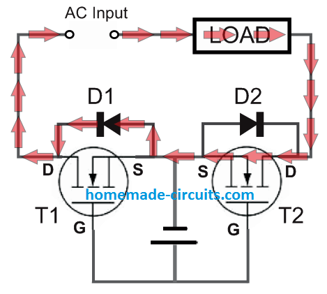
The working of the proposed sold state relay can be understood by referring to the following diagram, and the corresponding details:
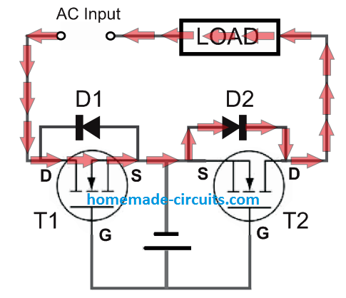
With the above setup, due to the input gate supply connected, T1 and T2 are both in the switched ON position. When the load side AC input is switch ON, the left diagram shows how the positive half cycle conducts through the relevant MOSFET/diode pair (T1, D2) and the right side diagram shows how the negative AC cycle conducts through the other complementing MOSFET/diode pair (T2, D1).
In the left diagram we find one of the AC half cycles goes through T1, and D2 (T2 being reverse biased), and finally completes the cycle via the load.
The right side diagram shows how the other half cycle completes the circuit in the opposite direction by conducting through the load, T2, D1 (T1 being reversed biased in this case).
In this way the two MOSFETs T1, T2 along with their respective drain/source body diodes D1, D2, allow both the half cycles of the AC to conduct, powering the AC load perfectly, and accomplishing the SSR role efficiently.
Here's an excerpt from the datasheet of the article.

Video showing the testing of the above SSR circuit
Making a Practical SSR Circuit
So far we have learned the theoretical design of an SSR, now let's move ahead and see how a practical solid state relay module could be built, for switching a desired high power AC load, without any external input DC.
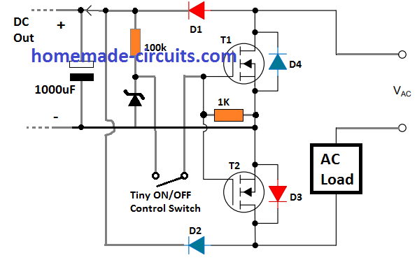
The above SSR circuit is configured exactly in the same way as discussed in the earlier basic design. However, here we find two additional diodes D1, and D2, along with the MOSFET internal body diodes D3, D4.
The diodes D1, D2 are introduced for a specific purpose such that it forms a bridge rectifier in conjunction with the D3, D4 MOSFET body diodes.
The tiny on OFF switch could be used for turning the SSR ON/OFF. This switch could be a reed switch or any low current switch.
For high speed switching you can replace the switch with a opto-coupler as shown below.
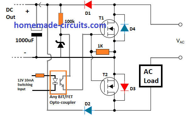
In essence the circuit now fulfills 3 requirements.
- It powers the AC load through the MOSFET/Diode SSR configuration.
- The bridge rectifier formed by D1---D4 simultaneously converts the load AC input into rectified and filtered DC, and this DC is used for biasing the gates of the MOSFETs. This allows the MOSFETs to get appropriately turned ON through the load AC itself, without depending on any external DC.
- The rectified DC is further terminated as an auxiliary DC output which could be used for powering any suitable external load.
Circuit Problem
A closer look at the above design suggests that, this SSR design might have problems implementing the intended function efficiently. This is because, the moment the switching DC arrives at the gate of the MOSFET, it will begin turning ON, causing a bypassing of the current through the drain/source, depleting the gate/source voltage.
Let's consider the MOSFET T1. As soon as the rectified DC begins reaching the gate of T1, it will begin turning ON right from around 4 V onward, causing a bypassing effect of the the supply via its drain/source terminals. During this moment, the DC will struggle to rise across the zener diode and begin dropping toward zero.
This will in turn cause the MOSFET to turn OFF, and the continuous stale-mate kind of struggle or a tug of war will occur between the MOSFET drain/source and the MOSFET gate/source, preventing the SSR from functioning correctly.
The Solution
The solution to the above issue could be accomplished using the following example circuit concept.
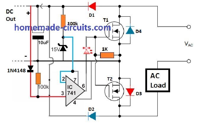
The objective here is, to make sure that the MOSFETs do not conduct until an optimum 15 V is developed across the zener diode, or across the gate/source of the MOSFETs
The op amp ensures that its output fires only once the DC line crosses the 15 V zener diode reference threshold, which allows the MOSFET gates to get an optimal 15 V DC for the conduction.
The red line associated with pin3 of IC 741 can be toggled through an opto coupler for the required switching from an external source.
How it Works: As we can see, the inverting input of the op amp is tied with the 15V zener, which forms a reference level for the op amp pin2. Pin3 which is the non-inverting input of the op amp is connected with the positive line. This configuration ensures that the output pin6 of the op amp produces a 15V supply only once its pin3 voltage reaches above 15 V mark The action ensures that the MOSFETs conduct only through a valid 15 V optimal gate voltage, enabling a proper working of the SSR.
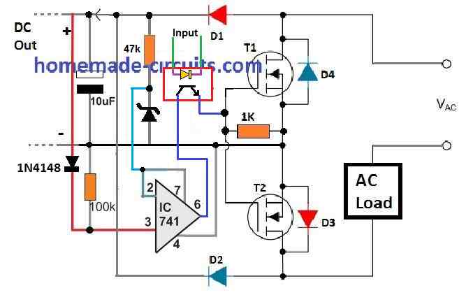
Isolated Switching
The main feature of any SSR is to enable the user an isolated switching of the device through an external signal.
The above op amp based design could be facilitated with this feature as demonstrated in the following concept:
How the Diodes Work Like Bridge Rectifier
During the positive half cycles, the current moves through D1, 100k, zener, D3 and back to the AC source.
During the other half cycle, the current moves through D2, 100k, zener, D4 and back to the AC source.
Reference: SSR
Hello, I’m building/have built a circuit that takes a 50hz ac signal from a class ab amplifier circuit and puts it as the ac input to a n channel fet relay as per fig. 3 above. I’m using a fod 3180 as the driver for the fet’s and so far everything works fine. Where I’m having issues is that I’m using a 555 timer to turn on and off the fod 3180 at about 1khz. On the positive half of the cycle the ac is shut off as expected, as a series of steps up and down the waveform; however, the bottom half of the cycle is unaltered, it’s just a negative sine wave.
I have to admit I’m just about at my wits end on this one. Do you have any idea why the negative half cycle doesn’t turn on and off like the positive half?
Thanks for any help you may provide.
Hi, did you connect the sources of the two MOSFETs with the negative (ground) of the IC 555? And I think a MOSFET driver is not required…you can directly feed the pin#3 of Ic 555 with the gates of the two MOSFETs
Hi Swagatam,
No, I didn’t connect the sources to the neutral ground and I used the driver because I thought that I read in the article that when you use N-channel FETs a driver is necessary in order to charge and discharge the gates of the FETs.
Thanks for the advice, I’ll try it and see how that works out. I’ll let you know if it works.
No problem Kurt,
Initially just connect the pin#3 of the IC 555 with the common gates of the MOSFETs, and connect the common sources with the negative or ground of the 555 circuit, also make sure to connect a 1k resistor between the gates and sources of the MOSFETs. A driver is necessary only when the load current is very high…
….I think you are right….a gate driver is strictly required for this application.
Please refer to the following post and check the following and read the “Using N-Channel MOSFET” section:
https://www.homemade-circuits.com/bidirectional-switch/
hie this diagrams are using DC 12v to genarate AC . can you provide me with a diagram which uses DC 400v to genarate AC . thanks
This circuit is not generating AC, it is controlling an AC load.
Hi, having minimal knowledge of electronics, I was wondering if the final circuit would be able to work safely on 240VAC power input and an 800W resistive load.
Hi, the above concepts are recommended only for experts in the field, not for newcomers, so I won’t recommend it to you.
If your load is a resistive load, then it can be simply controlled through a single MOSFET and a bridge rectifier, no need of the above complex design. Let me know if you would like to see the full schematic.
I have a 3d printer hotbed (resistive load 4 x 200W) and this should be controlled using PWM. So I was trying to find a solution for that, and discovered you article which seemed fit for my case. If you think that another simpler circuit, could make it work, I would like to have the schematic.
In any case, thank you for responding!
I think you should try a dimmer switch circuit such as this for PWM controlling of your load:
https://www.homemade-circuits.com/simple-ceiling-fan-regulator-circuit/
Your diagram is completely wrong. I don’t think you know what you’re talking about at all. When the MOSFET is on, current flows through the channel, not the body diode.
I know the current flows through the channel, the main thing is that, does the above concept work as intended in the application, or not.
Hi , I have a question .Is there anywhere I can find a Power mosfet Solid State relay for 20 amps using 120 VAC for sale or at least PCB kit ,maybe even pcb layout with , if possible a GERBER file, so I can order the production of a prototype Mosfet SSr for A C ?
Thanks in advance
Hi, you can try the following modified version of the first circuit: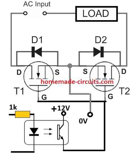
" rel="ugc">
However, I do not have the PCB details for this design.
Thank you very much !!
Hi sir, hope all is going well. Sir i need your
kind support. I want to make 40amp ssr.can you provide me diagram with components plz as usual in easy way plz
Hi Ghulam, what type of load do to want to control with the SSR, AC load or DC load?
Sir i want to run AC load, i tried with bt136, but as you know bt136 can’t handle heavy load…..i have bta41 800B. So plz guide me with diagram and components which is required. Plz
Thanks
Hi Ghulam, yes you can use BTA41800, it is rated to handle 40 amps load.
I hope you are referring to the following design
" rel="ugc">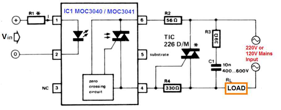
Yes sir same i want, sir what is the value of R1?all resister required qaurter watt? Sir can i use moc3021?sir plz guide me with diagram of bta41 800b. I dont have TIC 226 D/M plz
Thanks
Ghulam, R1 can be 1k 1/4 watt if the input voltage is between 5v and 15V.
All other resistors can be 1 watt CFR.
Yes MOC3021 can be also used.
The shown triac can be replaced with your specific 40 amp triac, no issues.
MT1 will go to the R4 side and MT2 will go to the R2 side.
Thank you sir, i will try and update you.
Sure, no problem, Ghulam.
Hello Sir, great document Thank you for everything.
I have a question please, can we use the basic circuit to connect or disconnect a series of 200v photo voltaic panels?
Thank you again sir
Thank you Laurent, you can use the basic circuit to connect or disconnect PV panels, however the above circuits are meant for AC supplies and loads, for DC supplies, like from a PV systems, you can employ a simpler design using a single MOSFET.
Hi , my name is Helder , I am trying to find power Mosfets S S Rs, for a project where I can’t use Triac SSRs, maybe I am looking at wrong places , I just can’t find MOSFET SSRs for A C voltages on AC currents like 10 to 15 amps , any help would be greatly appreciated
Hello Helder, the circuit explained in the above articles specifically designed to handle AC inputs, so you can use the above circuits with AC supply and AC loads.
One minor issue with the explanation of the circuit is whether or not current is conducted mainly through the body diode in the “reverse” MOSFET or whether it goes through the channel. Your second figure suggests that this current goes through the body diode but in most practical circuits, it won’t. The channel of a MOSFET can conduct in both directions when the gate is appropriately biased. Placing a voltage on the gate creates a conducting channel between the drain and source which acts like a low-value resistor. If your gate drive is adequate for the MOSFETs involved and they are sized appropriately for the current, the forward drop across the channel resistance is likely to be far lower than the forward voltage of the body diode, so the diode won’t turn on and will pass negligible current whilst the vast majority of it passes the the channel just like it does in the “forward” MOSFET.
Thank you for your quick response. Sorry to hear you haven’t yet designed one. If and when you do, will I be sent an email letting me know?
No problem! Sure, I will!
Interesting subject. Thank you for requesting questions.
Magnetic switches are essential for power equipment safety (table saws etc). Much of the older equipment, that is still effective, continues to be used but are not so equipped. Magnetic switches are expensive and, I’m sure, could be replaced my electronic ones. Have you designed/made such a switch that might be used for 120v or 240v single phase circuits?
Hall effect sensor and reed relay are the electronic magnetic sensors, but they require an additional electronic circuit to work. I haven’t yet designed a specific circuit using these sensors for the mentioned application.
¡ Exelent articule !
can this be used to switch audio signals of high power, 100W output ?
yes, it can be used..
Hi Swagatam. Great Article. Can you please tell me if i can provide the PWM signal to control the AC Voltage level through the circuit shown in the last diagram? My intention is to perform dimming of AC lights and control fan speeds using a microcontrollers PWM. Looking forward to your reply.
Thank you MJ, according to me, yes you can use PWM to the last concept, but I don’t think the dimming would work on LED lamps.
I suppose you referred to LED lamps which are driven by DC voltage, is it? I was hoping that any AC driven load would (lamps, fans be it led or helogen) would be dimmed slowed via pwm input to optocoupler of the last figure.
I am referring to AC LED bulbs which have a bridge rectifier and a filter capacitor inside. The filter capacitor will not allow the PWM frequency to work, and the LED will continue to illuminate with the same intensity even while the PWM is applied. Of course at some lower level the LED bulb will start flickering.
Yes, I agree with that. The bridge rectifier effectively converts the AC in the DC if I am correct in those sorts of bulbs, is it? And that is the reason the PWM effect will not be translated down to the DC level. And if we need to dim them as well, as we need to have some sort of DC-DC buck-boost converter. For now, it is sufficient for me to know that the AC voltage, of appliances which are directly driven by AC, can be controlled by the PWM in front of the opto-coupler.
Yes, that’s right, the filter capacitor will not allow the PWMs to vary the LED intensity and therefore the LED will not dim.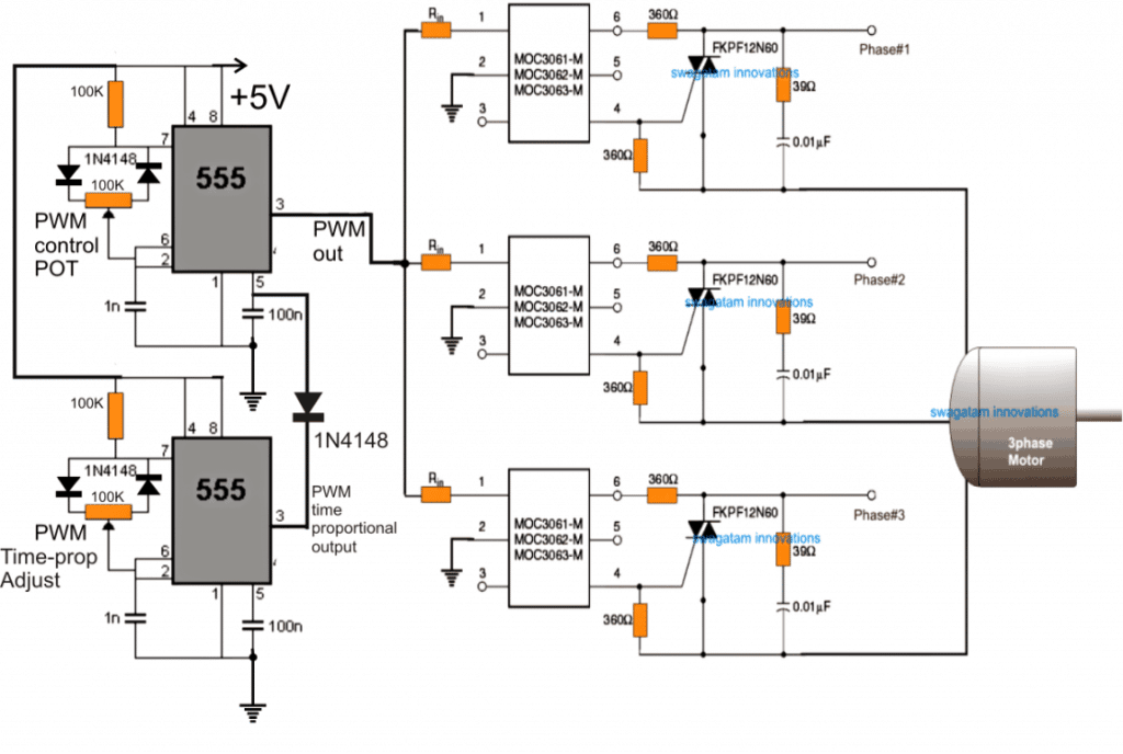
For other appliances you can simply use a MOC30XX series opto coupler with triac, which is much simpler to configure and use.
An example circuit is shown in the following diagram:
" rel="ugc">
You can remove the lower PWM 555 circuit and the two lower opto couplers for configuring a single phase PWM control on the load.
Thats great. Thanks a lot.
My pleasure!
Hello Swagatam sir,
I’m working on LED (powered by 230V AC) dimmer using MOSFET’s. I’m referring to this circuit
" rel="ugc">
While testing, the LED dims perfectly fine without any flickering but after turning the complete circuit off and checking the 15k (2W) resistors, they are getting very hot. I have read that resistive dropper circuits are not efficient but are used mostly for low current applications. Also in the article, it is mentioned the power rating of 15k resistor to be 0.5W & I’m using 2W.
What I’m assuming for now is that the MOSFETs do not have gate resistors & due to that the gate capacitor is causing a high current peak to charge its capacitor in order to switch on the MOSFETs. This may lead to heating of resistors. My assumption could be completely wrong.
How can I improve this circuit so that the resistors do not get hot as they are getting now?
Thank you
Hello Omkar,
The resistor will heat up for sure no matter what type of load you use. It is not because of the MOSFET gate resistor, rather it is because of the input and output voltage difference. The input is 230V and the output is 12V, this huge difference is causing the resistor to dissipate the difference through heat.
You can perhaps eliminate this issue by replacing the 15K resistors with a 0.22uF/400V capacitor.
But if you do this make sure to connect a 1N4007 diode immediately after the 0.22uF capacitor, with the cathode going to the capacitor and the anode to ground.
Thank you for your response.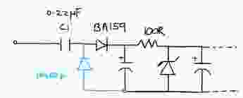
I’m attaching image of the connection you told, please check and tell me if there any changes.
Image – " rel="ugc">
You are trying to use capacitive dropper circuit to improve the efficiency?
Also do I need any extra components with what you told?
Thank you
That’s perfect! The BA159 can be also replaced with a 1N4007 according to me.
Yes, capacitive current limiter.
No additional components would be required.
Ok.
Did you calculate the value of the capacitor (0.22uF/400V) in this way?
If I put 0.22uF value in Xc=1/2.pi.F.C I get an impedance of 14.46k ohm. Also to drive the gate of MOSFET not much current is needed. So, by taking the max output current to be 15mA the voltage drop across the capacitor will be 15mA x 14.46k ~ 217V.
230-217 = 13V (which will be given further to the Zener diode)
What is the purpose of the diode you told to connect right after the 0.22uF capacitor?
In this circuit, the gate current not has to be provided constantly (only for the time the microcontroller is providing the signal). So, will this circuit be ok when there is no current requirement at the output side because the circuits that I have seen for a transformerless capacitive one, they are connecting a fixed load?
Please correct me wherever I’m wrong
Thank you
No I did not calculate because the MOSFET gate is a high impedance load so current is immaterial. Even a 0.1uF capacitor would work according to me for driving your MOSFET.
The capacitive power supply does not require a continuous load, it does not matter whether load is present or not.
The diode allows the 0.22uF capacitor to discharge during reverse AC cycle, otherwise the capacitor will get charged once and get blocked and will not provide the required output voltage.
I have also read that to limit the inrush current of capacitor (in this case 0.22uF)it is recommended a low-value resistor in series with the capacitor. But you didn’t told that because there is already a 100ohm 2W resistor in the series path of that capacitor, is that correct?
Also, I want to ask that for testing purpose if I can connect single 12V supply to both the dimmer channels? Because what I observed after looking at this circuit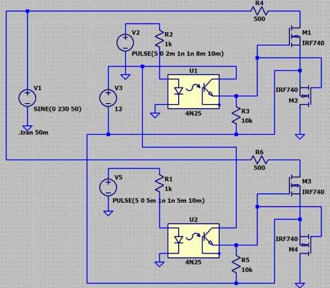
" rel="ugc">
that for example in the single 12V supply case when M1, M2 is off & M3, M4 is on then let’s say the current is flowing from +ve to -ve of AC. In this case, current will flow through R6 because both M3, M4 are conducting.
The source pin of M1, M2 & M3, M4 is now connected together due to a single supply. So now the current should also flow through the body diode of M2 towards the -ve side & this may lead to heating of M2 or anything else.
Also in another half cycle even if M1, M2 are not conducting, the current should flow through the body diode of M1 and further through R4 which is not intended.
Thank you
Yes that’s right, because of 100 ohm no other resistor is required.
I am actually having difficulty understanding the MOSFET configuration and working in your diagram.
You have a load for M1 and M3 as R4 and R6, but there’s no load for M2 M4?
Oh sorry, I didn’t give you the proper details.
M1 & M2 is a pair to control load R4. (2 MOSFETs connected back to back for AC circuit)
M3 & M4 is another pair to control load R6. It is a 2-channel dimmer circuit.
V3 is a 12V source (single supply) for both channels. You can ignore the PULSE source for now because that will be a part of the microcontroller.
R3 & R5 are gate pull-down resistors.
Source pins of M1, M2, M3, and M4 are connected together with the -ve of V3.
M1 & M3 have body diodes (not shown in the simulation), the cathode is pointing upwards. The same goes with M2 & M4 but the body diode is in opposite direction.
Is it ok to single supply for both the channels?
Thank you
No problem, so it seems your are using the MOSFEts like bidirectional switch, right?
I think a common 12 V will be OK for both the channels since the AC signal is also common and synchronized.
Yes, I’m using MOSFET as a bidirectional switch.
Yes, the AC signal is also common but after referring to this circuit-
https://docs.google.com/document/d/1M5DHuF4cN82JanBpeBDAEtk7uMGcdKistes7e4xeiL0/edit?usp=sharing
what I noticed is, for example M1, M2 are ON for only 1ms and M3, M4 are ON for 8ms. Then after 1ms M1, M2 should be off and no current should flow through them. But if you look at the yellow path then although M1, M2 is off, the current is flowing through the body diode of M2, because the source pin of all the MOSFETs is common and that is providing a path for M1, M2 to conduct.
The red color path is for the conduction of M3, M4
In -ve half cycle, the current should flow through the body diode of M1 and further through R4 which should not happen.
Thank you
OK, I can understand, but I ma having difficulty simulating the process in my mind therefore can’t suggest a solution to this problem.
Ok, no problem. I will test the circuit with what you have guided me till now.
Now I’m testing the circuit in which you told to connect a 0.22uF capacitor with a diode.
I’m having one doubt that in my circuit there are actually 2 grounds (One is the neutral & the other is the ground connected to the source pins of MOSFETs, these 2 grounds are not directly connected to each other)
So one end of diode is directly connected to capacitor & the other should be connected to which of these grounds?
Thank you
OK, I think to get rid of the confusion it is better to use a bridge rectifier with the 0.22uF. If you use a bridge rectifier then you get an isolated DC for the MOSFETs. Make sure to connect the 100 ohm resistor, the zener diode, the filter capacitor at the output of the bridge rectifier. If you use a bridge rectifier then no other diode is necessary for the 0.22uF to discharge. It can discharge through the bridge rectifier arrangement.
I have already tested this setup using a 12V AC source, it worked nicely. But in my circuit instead of a capacitive power supply I extracted the DC from the 12V AC itself. But anyway using a bridge rectifier should solve the problem for you.
Really sorry for my late response, I was busy with some other work.
Thanks a lot for your suggestion & I’ll surely take a look at it.
Also I’m having some confusion in selecting a proper TVS diode for my application. So, if you can help me in that part I’ll be thankful.
I’ll post my query regarding TVS diode in some time.
No problem Omkar,
However, I think selecting a TVS diode is a little complex and will require studying of the parameters of the diode.
I have found a very good article which explains how to select TVS diodes. Here’s the link for that:
https://www.ti.com/lit/an/slvae37/slvae37.pdf?ts=1680664959929&ref_url=https%253A%252F%252Fwww.google.com%252F
Thanks a lot for sharing this link, it is really helpful. Still I’m having one query. In some of my projects I’m using 5V-1A SMPS to power other electronics stuff & just want to make sure that the TVS diode recommended in their datasheet is proper for protection against any voltage spike. Till now 3-4 SMPS have stopped working and I’m assuming that TVS diode could be the reason for that.
The maximum AC input voltage given in the datasheet is 260V.
The recommended TVS diode given in the datasheet is P6KE550CA which is used to protect the input of the SMPS from any voltage spike.
1) The maximum clamping voltage given is 760V, what I understood is that if voltage spike appears then the TVS diode will clamp the voltage to 760V @ given Ipp and the SMPS will see 760V at its input. But the maximum input voltage for the SMPS is 260V, then is this safe for the SMPS? 2) The breakdown voltage given is 522.5V minimum. I read that breakdown voltage is the voltage at which the TVS diode starts to conduct/ starts protecting the circuit from spikes. For an example a voltage spike of 510V appears at the input of SMPS, because this voltage is less than 522.5 TVS diode will not start conducting as if it sees no voltage spike. But still 510V is greater than 260V, will it damage the SMPS? Can we use P6KE350CA/P6KE400CA to be more safe?
It is also written in the article that you shared the link for, that the clamping voltage should be nearby the working voltage of the device(considering some margin) to ensure more protection.
Thank you
You are right, the clamping voltage should be close to the maximum permissible input voltage of the device. For example for your SMPS the breakdown down voltage of the TVS diode can be around 270V and the clamping voltage can be around 300 v, otherwise the TVS diode is not going to provide any protection to your SMPS
For P6KE350CA, the clamping voltage is still very high at around 482V.
For P6KE400CA, the clamping voltage is 548 V again too high.
I am seeing that the breakdown voltages are much lower than the clamping voltage, so i am not sure what should be near the maximum device voltage, the breakdown voltage or the clamping voltage?
The SMBJ188A has a clamping voltage of 304 V which looks good, but a breakdown voltage of around 209 V which is too low.
Yes, selecting a proper TVS diode is a little tricky. Also thank you very much for your help till now.
I’m having one question regarding the protection of MOSFET & was reading your article – https://www.homemade-circuits.com/mosfet-protection-basics-explained-is/
While testing my circuit for AC light dimmer which uses two MOSFETs in series(in this way – " rel="ugc"> ), till now 2-3 times what happened is I’m getting a short across the drain & source of the MOSFET in both directions (forward & reverse bias of the internal diode).
In a new MOSFET, I get 0.5-0.7 V in forward bias & no reading in reverse bias which shows that the MOSFET is in good condition.
After replacing the MOSFET with a new one the circuit starts working again but I think this issue is nearby to avalanche protection mentioned in your article.
So, I think adding RC snubber/ MOV across the MOSFET would be a good idea. The max Vds voltage mentioned in the datasheet of IRF740 is 400V so need to select MOV around this voltage.
How can I calculate values of R & C to protect the MOSFET? Do you recommend any other type of components that can be used for protection?
Thank you in advance.
You are welcome Omkar, Is your MOSFETs blowing off due to surge current? I have not yet tested the above concept with 220V AC, I have tested it with 12 V AC only so i am not so sure about this situation. Also, calculating snubber can be quite tricky again, and I do not have the necessary formulas. Therefore I would recommend MOVs instead which are quite easy to determine.
Yes the clamping voltage can be below 400 V, maybe around 380 V, that might do the job. However if your MOSFETs are blowing without an MOV then that’s not a good thing. You can also try putting external diode across drain/source of the MOSFETs similar to the internal body diodes of the MOSFETs. I know putting external diodes does not make sense in this circuit since the MOSFETs can conduct both ways, still you can check the response by putting these external diodes whether these are able to provide any sort of avalanche protection.
I hope you have proper gate resistors installed with reverse diode, in series with the gates of the MOSFETs. Also make sure to have a 1K resistor installed across the gate/source of the MOSFETs.
I’m using this circuit for my project——–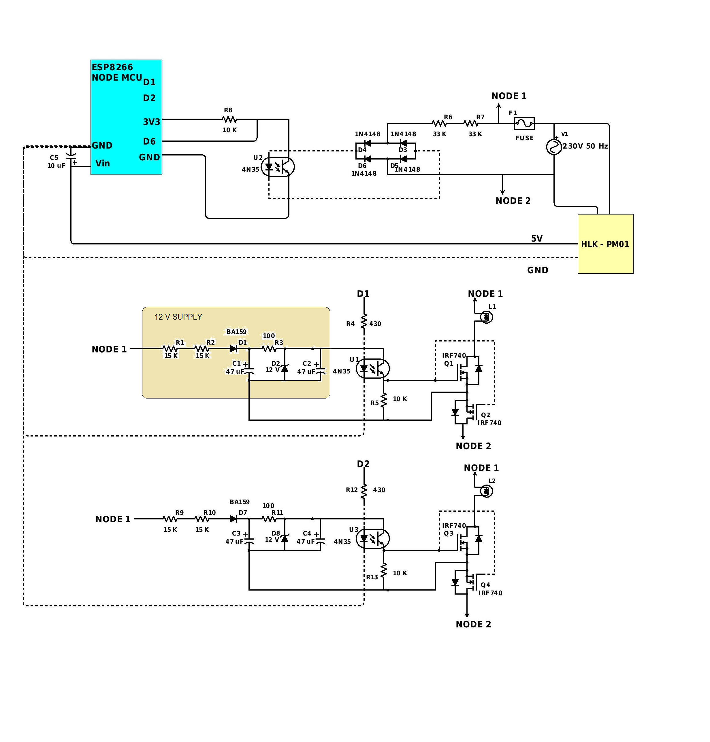
" rel="nofollow ugc">
I’m not sure if the MOSFET is getting damaged due to surge current. It can be one possibility of surge current. I’m also going to add a fuse in series with the MOSFET (also given in the reference circuit). In my current design I’ve not added the fuse (fuse can protect the MOSFETs from surge current).
Also as you said, I’m going to add a series gate resistor for individual MOSFETs.
I want to know the purpose of connecting a reverse diode in series with the gate of the MOSFET.
I’m not able to select a proper MOV for protecting the Drain-source of the MOSFET.
So I’m planning to use a TVS diode for that by changing the MOSFET number. Currently I’m using IRF740 as mentioned in the reference diagram. I can also use IRF840 after checking its datasheet. Because with IRF840 I’m able to select a proper TVS diode in that range.
I have connected a 10k resistor between the gate & source of the MOSFETs.
As you said also will try by connecting an external diode parallel to body diode.
I’m trying to make this circuit better than the current version & your response is helping me a lot.
The gate resistor and the gate diode may not be relevant for this diagram. The diode across the gate resistor is for enabling quick discharge of the MOSFET gate internal capacitance during the OFF periods of the gate switching frequency. But since here no frequency is used at the gates, it is a constant DC, the gate resistor and diode are not relevant and are not important.
The external diodes across the MOSFET drain/source is the only hope now and the TVS diode that you may be adding.
Okay.
Also there is no high frequency switching at the gate of the MOSFETs (only around 1KHz of PWM to drive the MOSFETs).
I have also read that for high frequency switching in order to provide a good turn on, turn off pulse & to reduce ringing a proper gate resistor is required.
So, as you said in my circuit it is not that important.
I will tinker with the circuit with what all discussion I had with you & will let you know.
Thanks a lot for your response.
I completely missed that the optocoupler is being used for the PWM input. In that case a 1KHz frequency is quite a large frequency, and the R5 and R13 are very high values which must be reduced to 50 ohms. Or alternatively you can try modifying the setup in the following manner by adding an extra transistor: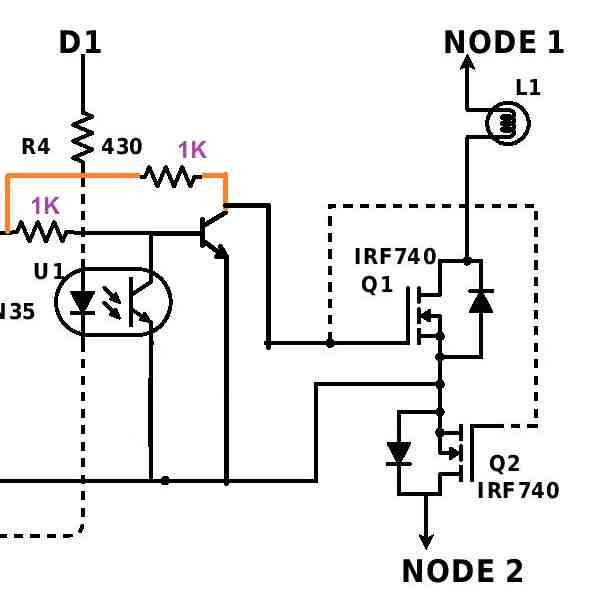
" rel="ugc">
The alternate circuit you have provided is for discharging the gate of the mosfet more faster and also to protect the gate of the mosfet by adding gate resistor?
Also I have one doubt –
Example when there is a high pulse at D1, internal transistor will turn ON and external will be OFF. Due to that the mosfet will get high at its gate.
When there is low at D1, internal transistor will be OFF and external will be ON which will connect the gate of the mosfet to ground.
The ground is also connected to one of the mains terminal (phase/neutral) through the body diode of Q2.
In this same article you explained me that there is no harm because only ground is connected to one of the mains terminal and +ve part is not.
So when external transistor is ON the +12V is now connected to the same terminal of AC where ground is connected. Is this safe? If yes how?
Thank you in advance.
If the ground connection looks confusing, then in that case you try a bridge rectifier instead of a single diode rectifier.
Ok, I will try that. But what I’m thinking is still the -ve of the DC part has to be connected to source of the mosfet which in turn will be connected to node2 (phase/neutral) through Q2 body diode.
Thank you
If a bridge rectifier is used then the there would be no issues according to me. Still, you can try confirming the present diagram through a transformer based power supply. If everything works OK then you can try the resistive transfomerless power supply with bridge rectifier.
Ok, can you provide me a reference circuit diagram for testing with a transformer.
Thank you
In the following circuit, remove the 15K resistors, and connect the 6 V or 12V AC secondary wires of the transformer with BA159 anode and the common line which connects with the ground side of the 47uF capacitor, and the 12 V zener diode anode.
" rel="nofollow ugc">
Thank you for giving the details about the connections.
I’ll let you the know the results for this and/or if I face any issue I will ask in comment section.
Sure, No problem!
The information about using MOSFET’s in AC circuits which you have provided is really good & useful.
What I really want to understand is why the -ve of your DC power supply (12V) & source pin of both MOSFET’s are connected together?
What happens if I don’t connect them?
The current which is flowing through the MOSFET is AC and it is connected to a -ve pin of DC power supply, I’m not getting.
Please guide me.
Thank you in advance.
Thank you for liking the article.
The gates of the MOSFETs require a positive supply to conduct with respect to their source terminals, which must be connected to the negative supply. If the source pins are not connected to the negative supply then the MOSFETs will not conduct or become forward biased.
Since both the MOSFETs are connected to a common 12V supply therefore their gate and source terminals are joined together.
Hope it helped!
Thank you for your response Swagatam sir. )
)
Ok, I understood why -ve of the DC power supply is connected to both of the source pins.
Now what makes me confuse is that ( I’m telling with respect to these
diagram – " rel="ugc">
Let’s say I have connected Phase wire to left of the AC input & neutral wire
to the right. In that case when I will trigger both the MOSFET’s then T1 will
act like a closed switch. Then the potential at source terminal of T1 will be
same as potential at Drain (switch is closed).
What I’m thinking is the -ve terminal of DC power supply will get 230V so is
this safe? If yes, how?
Please correct me if I’m wrong somewhere.
Thank you
Hi Omkar,
The DC source will not be harmed even while the AC phase is connected to its negative terminal.
It is because the positive source of the DC is isolated from the AC.
The battery or the DC source will explode only if both the terminals positive and negative are connected across the phase/neutral of the AC.
Consider the situation where you touch the mains phase wire with your hand wearing a non-conductive footwear on your feet. The AC will not harm you, but if your feet touches the ground then you may get an electric shock, the DC supply here also faces the same scenario.
Oh okay, now I got to know the reason.
Thank you sir, I really appreciate your help. In future can I ask my doubts in the comment section of this article if I face some other issue while testing this MOSFET circuit?
You are welcome Omkar, glad I could help! Let me know if you have any further questions.
Dear Sir
I want to switch dc voltage 35vdc to 250 vdc with Mosfet channel with Opto coupler due to isolaton require in application.Trigger voltage of opto coupler led is 3vdc to 24 vc max. pl suggest.
Hi Nitesh,
I have answered to your previous comments please check it out.
Hello sir
i want to control dc voltage from 50 to 150 vdc with mosfet via opto coupler with maximum trigger voltage of opto coupler led is 3 v to 24 v dc . pl suggest. It just on when trigger came & off when trigger pulse absent.
Hello Nitesh,
You can either use a linear control of the LED or a PWM control. In linear control you can use a series resistor with the LED and apply the DC between 3V to 12V maybe.
In PWM control you can apply a PWM to the LED with a series resistor.
In linear control the output transistor will heat up a lot during low voltage control (50V). In PWM the transistor will remain cooler but the PWM peak voltage will be always 150V, only the average voltage will be vary from 50V to 150V.
ok thanks. It is possible to shows schematics? i have a dc output voltage is max 250 vdc which is goes to mosfet drain & N channel mosfet turn on while led of opto get 3 to 12 vdc with series resistor. I want to go with linear control
I ill try to draw a schematic and upload it for you!
ok
You can try this circuit:
" rel="ugc">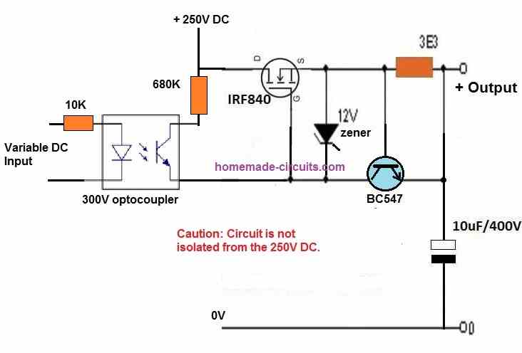
ok thanks . i will try & update
which opto coupler may i choose ?
You can search for 300 V transistor LED opto….you will many variants.
ok
pl suggest any 300 v opto coupler part number. Is 4N35 safe ? it data sheet shows 70v VBCEO . . when u used 680 k series resistor then can’t use 4N35?
4N35 will not be suitable even with 680k resistor. it won’t be safe.
You can Google search for 300V optocoupler, you will be able to find many options.
Thanks
hi dear sir i was looking a circuit that i can control through a 0 to 10 volt input,such as a PLC output .that i can creat variable voltage based on triac device with 220 voltage
i look forward to help you
Hi Sedigh, I do not have proper knowledge about PLCs, so it might be difficult for me to understand the concept and solve your query.
hello dear i do not mean circuit relation to PLCs
it was only to convey the meaning of the my request.Lamp light control circuit with 220 v and through triac but intead of using a potentiometer,use an input voltage 0 to 10 volts to control the light of the Lamp
Hello Sedigh, understood! You can try the following circuit, it should work:
Can we use this circuit as a Lithium-Ion Battery Cutoff switch? If we can do, then which changes would be required in this circuit.
I am not sure how the above circuit can be used as a Li-Ion battery cut off switch.
Swagatam, is there way to insure that switching always occurs at a 0V crossing (or near zero crossing)?
Hi Wes, which circuit are you referring to?
Dear Sir!
Can the switching of a mechanical morse be replaced by FETs?
To prevent the 2 connected parts from opening each other during ON-OFF? Thanks for the reply!
Hi Jozsef, yes, FET or BJT can be tried to replace the morse mechanical contacts.
Hello mr. Swagatam, no comment but a question.
Considering usage of your basic bidirectional SSR circuit, I take it that there N- Mosfets are being used.
Checking my ham shack spare parts I only find P-Mosfets.
My question: Is it OKay tot use these P-Mosfetd instead with the only difference to reverse the polarity of the Gates trigger signal ?
If not, what more should be done ?
73 PE0DVD
Hello Ad, yes it is possible to use P channel mosfets also….you can connect them in the following manner, and see how it responds:
Good morning mr. Swagatam,
Thank you very much sir
71 Ad
You are welcome Ad.
Hi,
What voltage the capacitor should be rated?
I simulated your circuit, and V on capacitor terminals raises almost up to the AC source’s peak.
Is this right or have I something wrong in my simulation?
I have some more questions if you what kindly answer:
1. Why the capacitor is only 10uF in the circuit with de op amp?
2. Why you lowered the resistor over the zener from 100K to 47K?
3. What does the new 100K resistor going to pin3 of the op amp do, is just for discharge the capacitor?
Thank you.
Hi, yes that’s right, the output voltage may be almost equal to the input peak voltage, however this may not be true also, because the moment 15V is reached across the filter capacitor, the MOSFETs would conduct causing the voltage across the capacitor to drop to almost zero. So the effective voltage across the output could be 15V DC
1) I reduced the value to 10uF since the charge value will be sufficient to hold the pin3 voltage to 15V for many milliseconds. Also this 10uF voltage can be increased upto 300V if required.
2) Because the current through 100k may not be sufficient for the zener to conduct.
3) It keeps the pin3 of the op amp referenced to the relevant supply line which is a standard practice for all opamps and CMOS ICs.
Hi Swagatam,
Looking at the back-to-back MOSFET relay for AC load you have provided in this example, How do you think about its advantage over Triac Relay on Inductive/Capacitive load? Can MOSFET relay survive without a snubber circuit if an inductive device is wired up to the load size?
Thank you very much for your attention.
Dang Dinh Ngoc
Hi Ngoc, the MOSFETs already have an in built diode so the effect of reverse EMF is minimal for these devices, moreover today’s mosfets are much more advanced with their protection features than the triacs.
Hi
you have great ideas.
need you help to design bi directional switch (MOSFET) . i need to pass thru in both directions signal (analog) that might have spikes up to 300V ,RDS On for both MOSFETS together is less than 10 Ohms and SW time is less than 80uS.
will appreciate your help
Thank you! the required circuit is already explained in the above article….you can customize it according to your own needs!
thanks, my problem is that i dont know which components to use in the design.
like part numbers of components and which design to select (i think that the NMOS because its low RDS On)
will appreciate any help here 🙂
many thanks
eli
You can try the first circuit initially using a battery for the gate/source switching, which will confirm the basic working of the bidirectional mosfets. You can use IRf540 for the mosfets.
If everything works fine, then you can assemble the last circuit and check the response!
many thanks !
Hi Swagatam,
Do we need snubber circuit for this model (the last schematic)? I dont have sufficient knowledge to explain myself when the load is inductive and does spike kill the Mosfet?
Ngoc
Hi Dang, I don’t think a snubber would be required as long as the reverse diodes are rated adequately high. Still for better safety you additionally add a 1uF/40V capacitor right across the inductive load terminals.
Thanks Swagatam,
I am thinking of making a home switch with back2back Mosfet to turn on up to 700W AC loads (any type). Since I was noticed that MOSFET in saturation mode will have very low resistance. Will it be possible to make mosfet relay without heatsink?
It seems that MOSFET relay should be more expensive than triac Relay?
THank you very much for your attention!
Hi Dang, MOSFETs will heat up when the load wattage is high enough….so if your load wattage exceeds the MOSFETs optimal threshold, then the device will heat up.
Yes MOSFET SSR is expensive than triac SSR.
The statement that the load current will pass through the body drain diode of one of the mosfets when the circuit is conducting is wrong. If a n-channel mosfet gate is biassed and the channel conducts, the mosfet channel will conduct in both directions. Due to the presence of the diode, it will only block in one direction.
Commenter is correct … MOSFET Drain-to-Source is directional (and if you think of it in terms of the Field Effect on the device Channel, it makes sense that the channel cannot sense the applied polarity) … BUT … the intrinsic diode is what prevents a single device from functioning as an bi-directional SSR. When the SSR is ON, both MOSFETS conduct bi-directionally. When the SSR is OFF, it relies on whichever intrinsic diode is reverse-biased to block, since the other will be no help (forward-biased). Which FET’s diode does the blocking depends on the polarity being applied to the SSR.
Yes,what you said,I think, is correct.
Good day Swagatam, well done Sir, please I want a circuit using MOSFET to operate as relay to have NO and NC with common function.
I want to avoid the clicking sound of relay, thanks
Thanks Seun, you can try employing the following design:
Solid State Relay (SSR) Circuit using MOSFETs
This guide contains the same lame error as multiple appnotes from TI. MOSFET body diodes never conduct when MOSFETs are open, and they are always open simultaneously. Here is fixed article on TI forum where audience noticed the mistake and it was fixed. It’s appaling that TI never bothered to fix appnotes for years. https://e2e.ti.com/blogs_/b/industrial_strength/archive/2016/07/26/a-modern-approach-to-solid-state-relay-design
Hi friend! I really enjoyed the class, it was magnificent; his way of narrating is that of a great Professor.
I would like, if it were possible a tip on how to create a circuit to keep the soldering iron of 30w, with an ideal temperature, constant. Thank you for the class and Congratulations!
Thank you friend, you can use the second circuit explained in the following post:
https://www.homemade-circuits.com/fan-speed-controller-for-heatsink/
Hi !
What is AC load?
Any appliance…
Hi Swagatam,
I have few doubts referring to the figure 2 of current flow.
1) since both the mosfets are turned on at a time the current should flow from both the mosfets rather than the diode, though the current only flows from the drain to source and not from the S to D, it taken a path from the diode please correct me if I’m wrong.
2) when the gate is powered or triggered with the DC supply voltage and the positive half cycle AC signal is passed from the mosfet, since the negative terminal of the DC supply is connected to the common source then why the positive half AC signal did not taken that DC supply ground path rather than flowing through the diode.
please let me know the above doubts I’m new to the electronic design thanks.
Hi Steven,
1) the current will take the easiest path which is through the forward biased diode, and therefore the associated MOSFET will remains completely ignored and turned OFF
2) Referring to the first diagram, the opposite pole of the AC is across its own supply points not the DC negative, so it will flow towards its own negative/positive points not the external DC negative. The points indicated as “AC Input” are referenced with each other, not to an external DC
Hi Swagatam
I have been looking for ideas to allow the use of FETs on AC lines, and these ideas have sparked my interest.
But isn’t Stephen correct that both FETs will be switched on simultaneously, and the (FET) diodes are redundant as FETs conduct current on both directions? (I am aware that TI indicates current flow though a FET diode, but with both FETs on the diode would be bypassed.)
Diagram Labelled ‘The Solution’
I am a little confused about the voltages on the 741 OpAmp pins. The capacitor will have the peak AC voltage minus 1 diode voltage drop, and a little ripple depending upon current draw. The OpAmp power supply voltage will be around 15V, limited by the zener. The non-inverting input will have the same voltage as the positive power supply. The inverting pin will have the rectified and smoothed AC line minus a couple of diode voltage drops. For a 230Vac supply, that peak would be 325V.
Forgive my stupidity, but I do not understand the operation of the OpAmp, the voltages on the pins of the OpAmp and timing of the FET switching.
Take care,
Mike
Hi Michael,
I have tried to explain what I have studied and understood in the ti.com article, so these are not my own ideas. You are correct, after going through some online artciles it seems the mosfets act like low value resistors, and the current pass through the mosfets rather than their body diodes.
But then I have a few questions which are as follows:
1) If the diodes are not used then why are they shown inside most mosfets? What s their actual use?
2) During an avalanche reverse current flow through mosfets why these diodes are referred to as the protective elemts, which protect the mosfets from avalanche current.
3) If mosfets can conduct either ways without the body diodes then what is the need of using two mosfets for the bidirectional SSR, why not do it using a single mosfet?
To answer your second question….the peak across the zener diode will never reach 310V even if 230V is used as the AC input. It will be always restricted by the zener diode voltage, because the moment the zener voltage reaches 15V, 741 pin3 becomes higher than its pin2, and the 741 output becomes positive, this switches ON the mosfets which conduct and bypass the current to the op amp and the zener, cutting off the voltage to the op amps until the next cycle arrives.
Hi Swagatam,
The diodes are intrinsic to the MOSFET, i.e. they are created as part of the manufacturing process. So they are present whether we like it or not. That is why two MOSFETs are placed back-to-back, so that one intrinsic diode is reverse biased on the positive half cycle and the other is reverse biased on the negative half cycle ensuring the FET switch combination does not conduct until switched on via their gates.
If 1 MOSFET was used then its intrinsic diode would be forward biased on one of the half-cycles, no matter which way around it was connected. If there were no intrinsic diodes then only 1 MOSFET would be required.
The intrinsic diodes are often of use when switching inductive loads, such as in an H-bridge. An external protective (free-wheeling) diode can be omitted but sometimes the intrinsic diode does not behave as well as an external diode so an external diode can be used in addition to the intrinsic MOSFET diode.
As both sources are connected together and both gates are connected together, then the gate-source voltage is always the same on both transistors. Therefore they are both either switched on at the same time, or off at the same time.
Thank you for the explanation of the OpAmp voltages. Would it be possible to add some diagram of the voltage waveforms, so idiots like me can see this better?
Take care,
Mike
Thank you very much Mike,
That’s very well explained, and has cleared all my doubts. Nevertheless I wouldn’t change the diagrams in the article, as it somehow helps to understand the conduction process of the mosfets with the help of the intrinsic diodes, and moreover modifying the article would be a lot of hard work for me.
Regarding the op amp question, I think you are correct, due to the presence of the 10uF capacitor, the voltage across the DC line would eventually reach 310V peak, and this would also reach the pin3 of the IC 741.
To rectify the issue we could probably do a few changes in the diagram.
We can allow pin7 to get the 15V from the zener, clamp the pin2 with a separate resistor and a 12V zener diode, so that pin2 now is fixed with a 12V reference, and next add an additional 15V zener across pin3 and ground.
Also the 10uF filter capacitor will now need to be rated at 400 V.
The waveform now can be a 310V DC across the DC out lines, and a AC 230 V across the AC load.
Do you think it makes sense now?
Hi Swagatam,
Thanks for the work you have done on this.
But I am horrible when it comes to ‘visualising’ signals.
I will ask one question.
What is Ground?
That means different things, in different circumstances.
I would argue here that ‘Ground’ is whatever voltage is on the FET sources. And this voltage is the mains input, which is altering between +325Vpeak and -325Vpeak (for 230V RMS).
And I don’t think we can say that ’15V is applied’ to OpAmp pin 7. All we can say is that pin 7 will have a voltage 15V greater than the FET sources.
As the voltage on the FET sources is AC – varying from -230V (RMS) to +230V (RMS), then the voltage on pin 7 of the OpAmp will (or might) also vary from -230V +15V (325peak+15, or 340V) to -230V +15V (-325+15, or -310V).
But…
But the voltage cannot be greater than the input peak voltage, so the voltage on pin 7 of the OpAmp can never reach +340V. (Which also means that the gate voltage cannot be 15V greater than the source to turn on the FET at this point.)
And when the input (AC) voltage swings negative, the voltage on the sources will go to around -325V peak. With +325V still on the capacitor…
Well, I’m not sure pin 3 of the OpAmp would like that very much.
And when the FETs are off, what voltage is on the sources?
But I might be missing something. I often do.
But there must be a way to create a gate switch on voltage that would track the varying voltage on the sources. Hopefully a simple way. Hopefully a way that does not need to be ‘topped up’ at regular intervals, because this would interfere will a configuration where the FETs need to be switched on for a long time.
Take care,
Mike
Thanks again Mike for your detailed explanation and expert hints on the subject.
Yes the ground here refers to the negative DC line which joins the sources of the mosfets.
I designed the op amp based ssr by referring to the ">ti.com suggestions, in which they have said that the 4 diodes work like a bridge rectifier, regardless of whether the mosfets are turned ON or OFF. And I assumed that the DC from this bridge rectifier could be used to power the mosfet gates.
I am actually having difficulty understanding and simulating your explanation regarding the voltage swings across the various points in the circuit.
However after reading you explanation I now feel that there are certainly some confusions in the op amp ssr design and the design may have some flaws.
As you said there should be a simpler way of creating the SSR design, after some thinking I could come up with the following simple design. I hope this should do the job as expected from an SSR. Let me know your thoughts on this.
Hi Swagatam,
I took a quick look at the link you provided (" rel="ugc">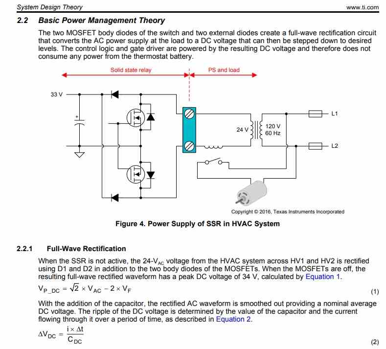 ).
).
Might an idiot like me make a few comments?
1) The text seems to make two claims that contradict each other
(a) The control voltage is provided by the FETs, in conjunction with two separate diodes
(b) The control voltage is used to switch the FETs
If there is no control voltage (at the beginning) to switch the FETs, how can the FETs create the control voltage?
2) In your mind, remove the 2 FETs. The remaining 2 diodes form a full-wave rectifier. The FETs are not needed for this, despite what the text suggests.
3) Both FETs switch together, as both gates and both sources are connected. Therefore the FETs would short out the AC supply when switched on.
But perhaps I am just being particularly stupid today.
Thoughts on your new design…
1) There could be a large inrush current if the supply was connected (switched on) at the peak of the AC waveform. A small value series resistor – maybe 100 Ohm 1/2W – might be useful
2) it might be good idea to put a bleed resistor across the 400V capacitor, to bleed off any stored voltage should the supply be disconnected (switched off) at or near the AC waveform peak.
3) The ‘Neutral’ of the AC supply is at or near the ‘Earth’ voltage. (These are connected together at the point where the mains enters the building.) Connecting the FET sources to another ‘Ground’ and connecting this to the bridge output ‘ground’…
Well, I am not good at visualising waveforms as I said earlier, but this doesn’t look quite right.
Hi Michael, You are right the FETs would switch together and short out the AC supply, so that makes the working even more confusing with respect to the 4 diodes. Honestly I am finding it difficult to simulate the whole process in my mind.
Regarding the new design, I was also worried about the inrush current that’s why I used a small value 0.1uF capacitor which might create an inrush only for microseconds and the 1 watt zener diode might be quite effective in neutralizing it, but as you said adding a 100 ohm resistor would be safer option. A bleed resistor across the capacitor also recommended in order to discharge the capacitor and safeguard the user from a possible momentary shock, when the unit is unplugged from the mains.
I am quite confident that this circuit will work. According to me the bridge rectifier does the trick here and it effectively creates a separate DC for the MOSFET gates. I wish somebody builds it and tests the results.
Hi Swagatam,
Instead of trying to visualise signals and waveforms, let’s create an imaginary circuit.
Let the upper AC input be the AC Live (Hot) and the lower AC input be the Neutral.
Let there be a load that takes 1A.
Let the ‘on’ resistance of the FETs be 0.1 Ohm.
Therefore the drain-source voltage drop will be 0.1V (when ON).
As the AC supply voltage swings between -325Vpeak and +325V peak, this 0.1V drain-source voltage drop is effectively nothing.
That means the voltage on the FET sources is the same voltage as the mains Live, assuming Live (or ‘Hot’) is connected this side.
The bridge ‘ground’ is connected to the FET sources. So the bridge ground is as the same potential as the AC Live. Further, the bridge +15V output must be 15V greater than the bridge ground, or +15V greater than the supply, to be able to turn on the FETs.
But this cannot be.
Now let’s make the upper AC input the Neutral, and the lower the Live. (Swap the 400V capacitor onto the ‘new’ Live also.)
The FET sources are now almost at Neutral (0V) potential.
The bridge output ‘ground’ is now 1 diode voltage drop higher than Neutral. If connected together, large currents can flow between the bridge ground and the FET sources. (Maybe this could be ameliorated with the use of a diode-resistor between these.)
So, this might work if use as a ‘low-side’ AC switch, i.e. if placed on the Neutral.
But, please, please, please, don’t take my reasoning as the law of the land.
These are just my ramblings.
I, myself, have been considering how to achieve this another way.
What we really need is an independent, ‘floating’, power source, where one side can be
connected to the sources and the other switched onto the gates as needed.
Would it be possible to use a transformer? A very small 230V-9V transformer? The rectified, smoothed, output of such a transformer would be around 12V, which would be perfect. The current required would be very small. Maybe such a transformer could be the size of an 8-pin DIP (such as a dual comparator or OpAmp), or maybe even smaller.
Research has, so far, shown that small magnetic cores seem to be all ferrite, which might not be the most suitable material for a 50Hz transformer. So I got to thinking…
How about stacking steel washers and using this as a core? Basic checks show that washers with a 3.2mm ID, 7mm OD and thickness of about 0.5mm are available. 50 of those stacked would be about 25mm (1″) tall, and about 7mm in diameter. The inner diameter would allow about 200 turns of 0.1mm wire without overlapping.
So…
Any thoughts Swagatam?
Take care.
Mike
Thanks Mike, I read your explanation, it makes sense and seems to be correct. I understand the working to a great extent now.
Surely a transformer based DC can be used and designing it is quite easy. But whether it is a ready-made transformer or a custom made transformer, these can be quite cumbersome and bulky. It is not required according to me.
An SSR is supposed to be very sleek, light weight and compact, so a transformer may not be a recommended option here.
A capacitive based power supply looks a better option to me.
Hi Swagatam,
Yea, transformer *can* be bulky. But the power requirement of the transformer would probably be less than 100mVA, and maybe a tiny fraction of that. It would be interesting to see how small this could be fabricated. If it could be made with the same PCB footprint as an 8-pin DIP or a bridge rectifier, or even smaller, then the solution would be no larger than those that use an OpAmp or a bridge rectifier.
I need a pair of switches to isolate the output of a grid-tie inverter from the grid. Unfortunately the bridge-zener solution would not work for this.
Take care
Mike
Hi Michael,
I agree a transformer would be a very clean method of implementing the ssr switching, and also it can be designed to be very small in size, but still we would have to calculate the number of turns, which could be a lot complicated, unless we do it do through some trial error.
If you know how to accomplish the number of turns then the problem can be quickly solved.
Hi Swagatam,
Sorry for not responding sooner, but I have been brutally tired of late.
I had hoped, based on your earlier responses, that you might be best placed to look at such a transformer.
Such a transformer – if possible – would also allow the isolated monitoring of mains level voltages by lower voltage control circuitry, which might be useful.
By the way, the ‘Reply’ button to your latest comments has disappeared, and I am using the ‘Reply’ button from earlier comments to respond.
No problem Michael,
Unfortunately I do not have the information regarding how to build a small low current transformer. I have a related article but that involves E/I core and the whole procedure looks quite complex. I think only a professional transformer maker would be able to provide a proper solution to this problem.
How to Make Step Down Transformers
The comment section is set to hold only 6 threaded comments, so may be after 6 replies the reply button disappears.
Hi Swagatam,
Perhaps it could be thrown out to the community for suggestions?
Spec:?
A toroid based small, low power transformer 230V – 9V 50Hz, maybe around 50mVA
Toroids can be stacked. The height of the resulting transformer can be as high as the tallest other device and it will take up no more enclosure space. (In my case, I have FETs mounted onto 50mm high heat sinks, with an overall height of about 60mm. So ‘small’ stacked toroids could be up to 60mm high and take up no more board space than a single toroid.)
Identifying the most suitable toroid material might not be easy, and is certainly outside my areas of expertise.
All the best.
Take care
Mike
Thanks Michael,
Yes I hope somebody will know how to build small customized transformers, and guide us through.
A alternative simple way is perhaps to stack up many small iron washers and wind around 300 turns for the primary and 20 turns for the secondary, using a thin copper wire, and then adjust the turns by checking the results.
Iron core will be most suitable since the AC mains frequency we use is 50 or 60 Hz.
Hi Swagatam,
My winter vanished over the space of a couple of days, and it is now time for me to put aside my winter projects and take back up with those outside. I have much to do there.
However, over these warmer months, I hope to be able to spend a little time ordering the items I would need for testing the concept, including the item needed for an inductor current saturation tester.
Perhaps we’ll meet again next winter.
Best wishes.
Mike
Thanks for the update Michael, hope you enjoy the summer months. Please keep up the good work.
Dear Swatagam
I love your site and its amaze me everytime thank you for opening site like this
Can you give a specific value of diodes?
Dc out? How much voltage needed for circuit first stage(capacitors,resistor,part)?
You say for fast switching add opto coupler so triggering opto coupler need another voltage input?
Thank you for your patience and answering <3
Thank you Trishpota, The diode rating will be twice of the load current rating. If load is 2 amp, then diodes must be 4 amps. Only 12V to 17 V DC will be enough for the MOSFET switching. Yes the opto will need to be switched externally from an external trigger source, because in an SSR the input and output is supposed to be completely isolated.
What about zener diode?
zener diode is 15 V, please make the last circuit which will ensure correct working of the SSR. Once confirmed you can break the red line and introduce an opto based switching through that line.
Hey Swagatam,
i am wondering how your rectifier can supply the Zener after the SSR has been switched on.
Imagine we are in the positive Half of the Sinewave.
If one of the Mosfets is swicthed on (lets say T1) then D3 of T2 is also in conducting mode. So lets say over T1 is 0.3V and over D3 is 0.7V then you have 0.3V+0.7V=1V for your Zener diode (after rectifier Diodes…), which tries to hold the OnState of the SSR. So, please correct me, but this will not work.
Best regards Tim
Hi Tim, During the half cycle before T1 can conduct the capacitor will be charged and this will hold the supply across the zener diode and also for the MOSFET gates.
Here’s the original link from where I referred the concepts:
https://www.ti.com/lit/ug/tiduc87a/tiduc87a.pdf
Thanks for your answer. Please have a look at page 12; “2.4 Undervoltage Lockout Design Theory”.
The cap will discharge as long as the SSR is in switched on and after some time it must be switched off to reload the cap again. So this is a good solution for something, that is switched on only for a short time, like a thermostat or something. The Texas guys seem to switch it at a certain point off and on again, so the cap reloads. Well its not a problem, but one have to know it before.
Nice article, how would you drive this from an Arduino if the load is 400 watts?
Then a totem pole would be needed to drive T1 & T2?
Glad you liked it, I think the last concept would be suitable for interfacing with an arduino
Hello, great tutorial, but I had a question. Since half of the time, the one mosfet has current going through its body diode which often has a voltage drop of 1-2V in the models I’ve seen, wouldn’t the mosfets get very hot for higher loads? Or do they not because they are only in this state half of the time? Thanks.
Hi, to ensure an efficient working you will have to complement the mosfets with more number if parallel mosfets
This is exactly what I want. However I need to switch AC on/off by means of 12v dc. If I connect +12v to the combined gates I don’t think it will work, will it? So how do I do this please?
It will work if you connect the the 12V DC across the gates and the sources of the MOSFETs as indicated in the first diagram.
You mean -12 connected to 240ac? Also if the gates are left floating will it switch of?
Tks for your help
yes that’s right….
gates must not be kept open…
I disconnected +12v from gates and have a 10k resistor between gates & sources but it’s still on,
so how do I switch it off?
Can be difficult to judge without seeing your circuit practically??
Hello Sir,
I have a question about this project. I like this project and may use it. However I would like to use something like this that would take the place of a standard SPDT relay for DC. Basically to replace the relays in one of your other circuits used to charge two 2 batteries flip-flop style. Thank you much for all you do.
Hello Joel, for a SPDT DC version you can probably try this concept:
https://www.homemade-circuits.com/12v-dc-solid-state-relay-ssr-100-amps/
Thank you I found it and it looks like it will fit just the way I wanted. I enjoy your site and play with your circuits to draw pc boards with. Just for fun.
Glad you are enjoying my site, please keep up the good work!
I have a question about the circuit that you directed me to. I have used your split 12v charger and the above mosfet circuit you directed me to, for a project I want to build. My question is by looking at what you showed me it seems that the mosfets switch the ground and not the positive side? If that is true the common is nothing more than the positive side of the battery? Y or N. Have not done much work with mosfets which is why I ask.
Thanks much for your help.
yes, that’s correct, even in a relay you have one of the load terminals connected to + or the – line.
Ok I thought so just wanted to make sure I was seeing things right. Thanks again
Swagatam: Thanks mate. In my 50+ years of work in the IT industry I have been taught many a lesson by the old “240”. Many faulty power switches, many incorrectly wired extension cables, many mistakes by unknown “dodgy” sparkies. I am still here, but I wonder if the fibulation I suffer from can be attributed to those “shocking” events…
Jeff
That’s awesome mate, I appreciate your knowledge and help! Please keep up the good work!
Sir can you give a system for a full bridge topology using 4 N channel mosfets?
Is this system suitable for powering inductive loads? The reason why I am asking this is because,power is rectified to DC before reaching the load.
All types of AC load can be powered, please see the arrow diagram.
I can see the arrows show that power passes through the forward biased diodes in either cycles,this will in turn be rectified to DC. Am I right or wrong?
The DC is rectified and used for the gates, not for the load. The load will be switched with the input AC only.
If I connect the gates directly without a switch,is there any issues?
The MOSFETs and the load will be permanently switched ON then.
Thanks you for publishing this, however I must make one very important point:
When dealing with the AC Grid mains, you must provide some sort of isolation between the low voltage trigger input and the mains. Maybe an opto-isolator or a reed switch?
Also, what is the purpose of the second circuit (with the 12 volt DC power supply?) How do the mosfets get triggered to control the AC load?
Note, that circuit requires isolation for the low voltage DC as well.
Thanks
Thank you, the SSR explained above is designed to derive the gate voltage from the load itself, not from any external source, therefore isolation is not necessary. Moreover the entire configuration is supposed to be enclosed inside a sealed module. Also the Opto coupler would require more current than a 100k resistor so that may not be appropriate for an SSR design.
The first two designs are for explaining the concept and the conduction path of the module. The battery sign at the mosfet gate shows a biasing DC input for the gate.
I am sorry…Yes an opto coupler should be added for an external low current switching, in my earlier diagram I completely missed that if the gates were connected with the 100K/zener output that would keep the SSR permanently ON. I have changed the design now for your reference.
Sir swagatam,any diagram with p channel mosfets?
pchannel is not recommended due to its higher resistance compared to N channel
Hello sir swagatam,help me understand;
1. 100k and zener act as voltage divider/step down?
2. I understand that during the positive half cycle,power goes through D1,100k zener and D3 back to load, so my question is, Can 12v zener diode and 100k hold a huge load say 5000w load ac?
3. Can I this idea be used to switch more than 200A DC? How?
4. Can this circuit be used as a 12v step down for inverter change over? Also how?
Evans, the 100k and the zener are for biasing the MOSFET gates, the load is switched through the MOSFETs and the internal body diodes and therefore can be dimensioned for switching any desired load.
Understood sir swagatam,I think was missing a point but got it. Now please correct me if I’m wrong, is it true that the load will be powered by dc since power goes through the mosfets internal body diode? If so , isn’t there any way this can be made to pass ac to the load?
The devices will conduct alternately for switching the AC input, please see the arrow diagram