In the following paragraphs I will try to explain the most basic foundations of digital electronic circuits: namely logic gates and logic flip-flops. Whether it is a complex and larger digital circuits, or as simple as a BCD counter, for example the 7490, or a large-scale integration (LSI) microprocessor chip, eventually all of these comprise of a many, and several types of digital-logic gates.
In this article we would be discussing 12 basic digital circuits, which can be used as building blocks for making complex digital designs.
Let us explore the features of all those fundamental digital circuits below.
Logic Families
Digital-logic families or integrated circuits are units that are structured or built using the common circuit components like transistors, capacitors, resistors, so that it becomes simple to interface them with each other through direct electrical conductors such as wires or PCB tracks.
The complex interfacing job is therefore eliminated since we don't have to think a lot about matching signal levels and impedance values etc.
The a couple of contemporary digital-logic families include the transistor-to-transistor logic (TTL) and complementary metal-oxide semiconductor (CMOS) devices.
The TTL logic ICs are built using NPN/PNP bipolar transistors or BJTs, whereas CMOS digital ICs are structured around field-effect transistors FETs or MOSFET's). It is possible to identify a CMOS IC through their "4xxx- series" part numbers (for examplle the IC 4049).
TTL ICs can be recognized by their printed numbers that begin with 74xx (for example IC 7490) or 74xxx (for example the IC 74161).
Military level TTL ICs are occasionally witnessed in amateur components vendors as industrial surplus. These ICs have the same printed figures like the ordinary hobbyist version, barring the the initial "7" which may be found substituted with a "5." Put simply, these have numbers like IC 5490 which may be equivalent to a 7490.
Digital Vs. Analog
Digital electronics is different from analog electronics with their characteristics of pulses or the signals that are processed. In an analog circuit, a signal may have just about any value across a particular range.
As an example, let's assume there's an opamp is connected for analog functioning. Furthermore, assume that it is possible for the output voltage to move from -12 to + 12 volts DC.
With an analog circuit, the output voltage can usually accept any value from -12 volts to + 12 volts; no supply values are barred.
On the contrary, digital circuits will accept only a single value out of the two permitted values, all the remaining values are prohibited. Due to the fact that in digital circuits only a pair of signal voltage values are acceptable, we express these circuits to be binary in nature.
Both of these levels are usually known as 1 and 0 (or logical 1 and logical 0), or simply true and false, or they may be also represented as high and low.
In this post, we will be using the terms "high" and "low" to indicate the various states, apart from for a couple of instances where 1 and 0 may appear to be specifically suitable.
There are two logic IC families or the digital devices that work with different voltage levels for high and low. One example is, the TTL logic IC family that functions using +2.4 to +5 volts for the high logic levels, and voltage or signal levels between 0 volts and + 0.8 volts, for low logic levels.
However, with CMOS logic family, you are able to work with absolutely any voltage or signal levels between -15 to 0 volts for low logic levels, and 0 to +15 volts for high logic levels.
Generally speaking, one of either scenarios are normal in CMOS circuits. Thus in CMOS ICs either we denote low as zero and high as +5 volts (in situations when interfacing with TTL becomes necessary), or low can be a negative voltage and high can be a positive voltage of the identical value.
The phrases "positive logic" and "negative logic" may at times mix up folks who are just understanding digital electronics. For logic systems that are positive, a high will be a more positive voltage than a low. In negative logic systems, a low will be more positive than a high.
Gates
The most standard digital component are the gates. Just about all digital circuits could be created by configuring just three of these standard gates: the NOT gate, the AND gate, and the OR gate.
Despite the fact that these three gates can fulfill most of the digital functions, we additionally incorporate the other popular gates namely the NOR, NAND, and OR gates amongst the basic ones.
While we talk about each of these gates, we will look at their schematic symbols, an equivalent circuit crafted from switches that switch ON/OFF a lamp, and its truth table (which tells us the conditions that determine 1= high and 0 = low).
Last but not least, we're going discuss about a wavetrain graphical example. You may want to analyze the wavetrain illustrations so that it helps you to gain an in-depth understanding regarding how these gates work in dynamic circuits.
1) Inverter Gates
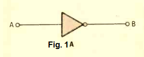
Inverters, which are also referred to as NOT gates. They are called inverters because they generate an output which is just the opposite of the input.
When the input signal to the NOT gate is HIGH input, the output generates a LOW signal, and vice versa. The alphabet "A" is used as an expression which symbolizes the input, therefore "A" can be applied with a high or a low. Similarly, the letter "B" signifies the output, and can be a high or low depending on the logic at "A".
An inverter gate is displayed with a triangle sign, having a tiny circle at the apex of the triangle, which is also the output of the gate (see Fig. 1A). Whenever we find a circle on any lead (input or output) of a digital circuit that signifies inversion, as we're going to learn the same with a few of the other gates.
Often we are able to obtain better understanding of a circuit functioning by exploring at its basic equivalent circuit. In Fig. 1B we find a straightforward DC circuit which symbolizes the basic working of an inverter gate.
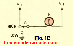
Switch S1 is positioned to select either a high signal (V +) or a low signal (ground or 0 volts) as being the input to the circuit. The lamp shows the output condition: a switch ON for a high output and switch off for a low output. While the switch is in the HIGH position, each sides of the lamp get exactly the same voltage difference, which causes the lamp to remain shut off.
This signifies a low output. As soon as the switch S1 is selected in the low position, the lamp obtains both ground and V+ therefore the lamp illuminates to demonstrate a high output.
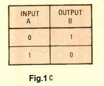
The truth table for the NOT gate can be found in Fig. 1C. Here we see that the input is A and the output is B, which means that a low input at A delivers a high output at B, and a high input at A delivers a low output at B.
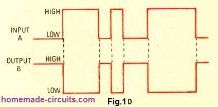
This circuit operation is demonstrated in Fig. 1D. Here, the A is the input, while the B or ̅A signifies the output. The line or the bar shown above the input or output in logic notation signifies an opposite signal to whatever the "unbarred" signal may be having.
As an example, if suppose A is high, then ̅A will be low. This notation allows us to signify the relationship between the input and the output as represented in the following expression:
B = ̅A
This is a manifestation can be found in Boolean algebra, and it represents the mathematics of digital logic.
2) OR Gates
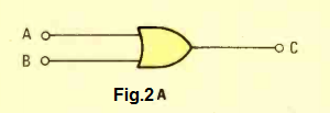
An OR gate (Fig. 2A) generates a high output when at least one of its inputs is high. Therefore when, A or B, or both A and B are high, then it gives a high output. An alternate way to explain this is, to get a low output from an OR gate, it is necessary for both of its inputs to be low.
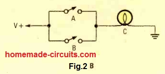
Figure 2B exhibits a clear-cut equivalent circuit for the OR gate. Here we see that the lamp (output) is switched ON (high) when either switch A "or" switch B is high. That is exactly why these gates are known as "OR" gates.
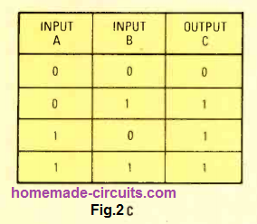
A truth table for the OR gate can be seen in Fig. 2C. What it affirms is that the output is low as long as all inputs are likewise low, and a high signal on any one of the both inputs generates a high output.
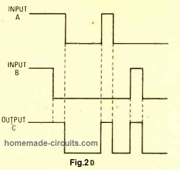
The behavior of the circuit with the above specified rules can be witnessed in a realistic form in Fig. 2D. Each of the inputs get a series of pulses, and the variations in its output demonstrates how the gate operates in accordance to these input levels.
3) NOR Gates

The NOR gate can be made by interconnecting an OR gate with an inverter gate or NOT gate. (Observe the ring around the output pin in Fig. 3A.) The gate could be described as a NOT/OR gate. The NOR gate generates a low output when any one or both of its inputs are high.
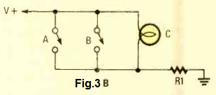
A comparable circuit for the NOR gate using mechanical switch can be seen in Fig. 3B. So long as each of the switches are in the open condition, the lamp remains switched ON, however if any one of the switch is closed then it causes the lamp to be switched off.
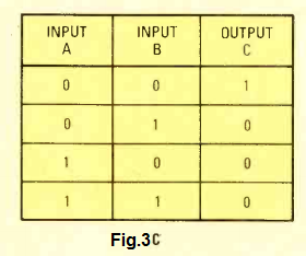
The truth table for this circuit can be witnessed in Fig. 3C, which may be understood in a nutshell through the following guidelines:
You will get a HIGH from a NOR gate output when, and only when, both of its inputs are supplied with low logic (meaning the output will be logic low only if any of its inputs is high.)
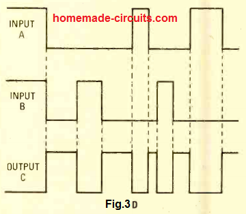
Talking about an NOR gates, the same regulations can be understood in a graphical manner as shown in Fig. 3D
4) AND Gates

The AND gate as indicated in the Fig. 4A will generate a high output in a condition when both its inputs are high.

We can witness a equivalent switch and bulb replicating the AND gate function in Fig. 4B.
The lamp is switched when both its switches A and switch B are turned ON.
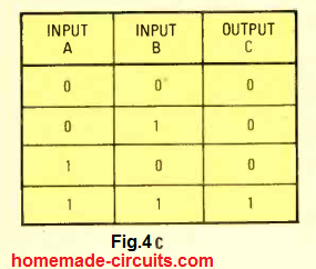
As given in Fig 4C we can summarize the truth table in the following manner:
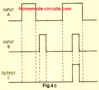
The output of an AND will turn low when both its inputs are is low and its output will be high only when both of its inputs are high). The very same rules can be described in practical circuits through the graphical diagram as depicted in the Fig. 4D.
5) NAND Gates

A NAND gate can be seen in the Fig. 5A which is yet another gate built with a combination of an AND gate with a NOT inverter gate.
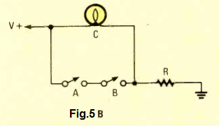
We can witness an equivalent lamp/switch circuit of the same in Fig. 5B.
In a situation when both the indicated switches are in the open state, the lamp will be switched ON. The lamp will be turned OFF only in a situation when both the switches are toggled OFF.
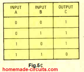
The appropriate functional rules for a NAND gate can be witnessed in the truth table as indicated in the fig. 5C. The same maye be comprehended at a glimpse by reading the following:
The output of a NAND gate will be high when one or both of its inputs are held low. In other words, the output of a NAND gate will be low only when both of its inputs are held high.
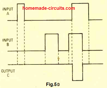
Just like in our previous examples, the same rules can be expressed in a graphical manner as depicted in Fig. 5D.
6) XOR Gates

This is last in the list of our basic standard gates which is known as the Exclusive-OR (XOR). That image of the XORR gate can be witnessed in the Fig. 6A which appears to be a bit uncommon, however it can be used for a plenty of practical digital circuit applications.
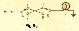
For a pictorial working circuit of this XOR gate you may refer to the Fig. 6B. The lamp/switch circuit is built using a a couple of SPDT switches interconnected with each other.
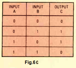
From the supplied the truth table as in Fig. 6C we are able to learn a few useful actions: When both the inputs of a XOR gate are low, then it provide a low output. In case both of its inputs are high, then we get an output that is yet again low.
In a situation when one of its inputs is applied with a high signal, and the other input is applied with a low signal, then the output produces a high signal.
To put it differently, the output will be low only in a situation when both of its inputs are applied with identical signals, meaning when both the input are either high, or both are low.
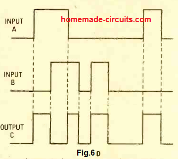
That working pattern of a XOR gate can be witnessed in the Fig. 6D.
7) Flip-Flops
A flip-flop can be understood as a one-bit memory device built using a few fundamental gates, however it is hardly given any importance today, due to modern technologies producing chips capable of handling 256KB and 1MB dynamic-memory ranges.
Nevertheless, for specific applications flip-flops continue to be widely used in digital electronics, both in computers related applications or even in circuits which don't have any connection with computers. Normally, flip-flop configurations possess a two outputs identified as Q and Q-not (or ̅Q).
The Q output works like the primary output, while ̅Q functions like a complimentary for the Q output. Meaning, if Q generates a high signal, then ̅Q will become low logic, and vice versa.
Additionally, whenever an input supply line on a circuit diagram drawing is indicated with a tiny ring on the body of the flip-flop, then it implies that input will be active when low. Or else, the input will be active when high.
8) R-S Flip-Flops
The R-S, flip flops which stand for "Reset-Set," flip -flop can be defined as a configuration which includes a pair of inputs: namely set and reset.
If the reset input is held in the active mode, the Q output is pushed to produce a low (if it has a ̅Q output in that case it will be pushed high). The set input generates exactly the reverse result: a positive input signal causes the Q output high and the ̅Q output low.
We can normally find two types of R-S flip-flop: NOR-logic and NAND-logic. The NOR-logic R-S flip-flop configurations are built using a pair of input NOR-gates for example by using the gates from the 7402 ICs.
The NAND-gate configurations are designed by employing Two-input NAND-gates, for example by using gates that are available inside the 7400 ICs.
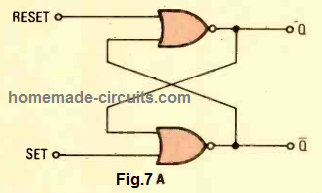
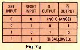
The NOR-logic flip-flop circuit can be witnessed in Fig. 7A, and the truth table for the same is provided in Fig. 7B.
The NOR logic configuration makes use of active-high inputs. To put it differently, when a low signal is applied on both of its inputs simultaneously, it causes no change or variations in its output. However in case, any one of its input is applied with a high logic, with a low logic applied to the other input, then this actions results in a change in its output-state.
What change in the state of the output happens will depend on which of the inputs (the set or reset) had been rendered active. Applying both the inputs simultaneously with a high signal is prohibited simply because in that case the output results can become unpredictable and unstable.
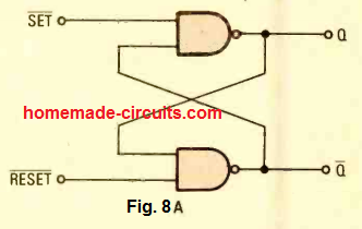
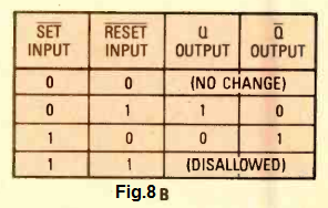
The NAND logic configuration as depicted in Fig. 8A works by using two-input NAND gates as opposed to NOR gates for creating a flip-flop circuit. They behave exactly oppositely to the NOR-gate flip-flops (you can compare the truth table results from Fig. 8B with Fig. 7B).
In NAND logic flip flop we find a couple of R-S flip-flop ICs obtained from the CMOS family of ICs. The IC 4043 is a quad NOR-logic R-S flip -flop ("quad" name is given since it includes four R-S flip -flop's internal to the IC).
Likewise, we have the IC 4044 which is a quad NAND logic R-S flip -flop.
9) Clocked R-S Flip-Flops
One of the main problems associated with R-S flip-flop configurations is that, any form of noise appearing on its inputs can cause an spurious chnage in the output state.
Additional issues associated with R-S flip -flop is that these are asynchronous or these are not time-dependent and can function simply in the presence of a legitimate input signal.
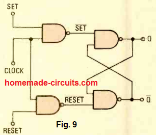
A remedy to these sorts of challenges can be the implementation of clocked R-S flip -flop configuration as shown in the Fig. 9.
The two gates on the right side constitute a NAND gate logic R-S flip -flop in the identical fashion as done in Fig. 8A. The control of inputs of this flip-flop are implemented by the outputs of the other two NAND gates.
For so long as the clock input stays at a low logic, the outputs of each of the left gates stay latched in the high logic mode, which means that the R-S flip-flop is unable to operate now.
However, if the clock pulse to the turns high, then the R-S flip flop outputs respond and change the output state either to set or to reset.
10) Master-Slave Flip-Flop
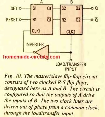
Another type of flip flop called the "master-slave" flip-flop, which is also known as the load/transfer flip-flop, can be seen in the Fig. 10. This flip flop configuration is built using two clocked R-S flip-flops, A and B as indicated in the diagram. The configuration is designed in such a way that the left side flip flop's outputs trigger the inputs of the right side flip flop.
The two clock lines are operated with signals that are out of phase with each other but the signals come from a common clock source, called the load/transfer, or the L/T input.
When the L/T line has a high signal, then the clock at the A flip-flop is turned low and the B side flip flop is turned high.
In this situation, B will be active, and A will be inactive. Whatever logic levels show up on the A outputs are instantly shifted to the B outputs on account of CLK2 being high.
However once the L/T line becomes low, flip flop B gets disabled (although its outputs continue to remain the same) and flip flop A becomes enabled. Any variations caused on the S and R inputs are reproduced on the Q1/ ̅Q outputs of flip flop A. When the L/T line is applied with a high signal again, these new quantities are shifted to the outputs of flip flop B.
The master-slave flip-flop is used in applications where noise or synchronization can be an issue. In certain flip-flops we find a differences between the clock triggering.
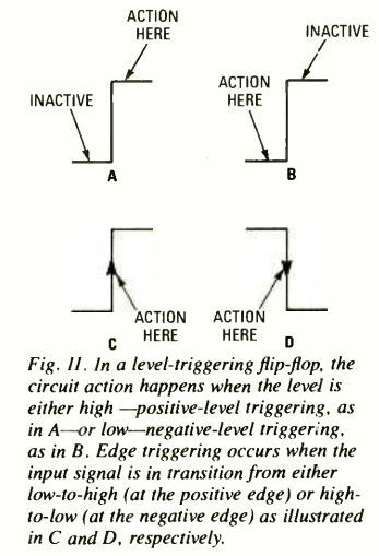
Figures 11A and 11B indicate the difference between positive and negative level triggering. With level triggering, the circuit reacts once the level is either high (positive-level triggering) or low (negative-level triggering).
Triggering at the edge of the signal happen when the input signal is just changing over from either low-to-high (referred to as positive-edge triggering), as in Fig. 11C, or high-to-low (referred to as negative-edge triggering), as displayed in Fig. 11D.
11) Type-D Flip-Flops
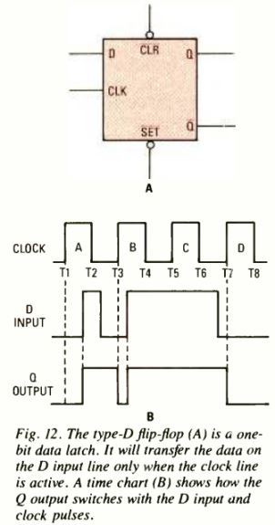
The type-D flip-flop, also referred to as one-bit data latch. As shown in the Fig. 12A it is a digital device designed to send the data on the D input line only in the situation when the clock (CLK) line is active.
In the majority of type-D flip -flop's, the clock is rendered active whenever a high signal is applied to the CLK line. Therefore the rule can be interpreted as:
The data level on the D input is delivered to the Q output as soon as there's a high signal on the CLK line. Hence, the type-D flip-flop is known to "latch" the D input data for one clock cycle.
In other words: As long as the CLK line has a high signal, the state of the Q output follows the D input. All of the transitions or the changeovers taking place at the D input are goes through an inversion (gets inverted) and then it is transferred to the Q output.
Meaning, a high signal at the input delivers a low output, and a low signal at the input generates a high output. In Figure 12B we are able to witness a graphical picture showing how the type-D flip-flop actually performs.
We find four clock pulses depicted as: A, B, C, and D. These are exihibited in the form of periodic square-wave string of pulses, but it is not necessary for them to be this much regular.
It is possible to connect the CLK line to an input source which only turns high occasionally.
Suppose the Q output is low at the beginning. At a time T1 the CLK turns high and the D input is low. As a result, the Q output will hold low during this period.
But remember, during the time pulse A is still high, the D input will make a sudden changeover to high. At this stage, the Q output instantly turns high and continues to be in that position after pulse A has terminated at time T2.
In a situation where the D input turns low again, the Q output would follow the sequence. You can take a look at the the rest of the pulses for understanding the relationship between the output and input levels in response to the the clock signal. Good examples of typeD flip-flop is the IC 7474 dual edge-triggered TTL flip-flop, and the IC 4013 CMOS device.
The IC 7475 is a TTL quad-latch device, however it includes just a couple of clock-inputs. Each one clock input is hooked up to a set of two flip-flops. If the two clock lines are joined with each other the 7475 functions like a four bit data latch.
12) J-K Flip-Flops
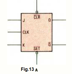
Fig. 13A shows an illustration of J-K Flip-Flop device which could be powered through one of the two methods: direct and clocked.
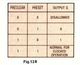
The truth table logic for the direct mode can be witnessed in Fig. 13B. While they are held in the low logic positions, the direct inputs of the device (clear and set) remain active. For implementing direct function the J and K inputs are usually attached to the inactive state. In this case the inactive state is low logic.
The working of the J-K flip-flop configuration depends on these inputs, and the clock input is unimportant (while held in the "don't-care" condition).
Observe that the figure indicates all four possible combinations of clear-and set-input states. In a situation when both set and clear are in the low logic, the J-K flip-flop is unable to "understand" what it needs to do, therefore this condition is forbidden. In this condition the outputs can be erratic, therefore such combination of inputs are no allowed.
In any situation while the clear input is applied with a low logic and the set input is applied with a high logic, in this situation the Q output quickly attains the low logic and the ̅Q output turns high. However as soon as the set input is applied with a low logic and the clear input with a high, the results turn opposite:
Q now becomes high and ̅Q becomes low.
Now observe how the device behaves when set and clear both the inputs are applied with high logic levels: the J-K flip-flop now gets organized in the clocked operation mode and we have a different set of rules being implemented.
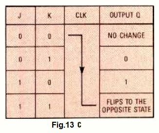
The truth table for the above discussed clocked operation for the J-K flip-flop can be learned from the Fig. 13C.
The J-K flip-flop works with a negative-edge triggered clocks. Meaning , the output changeover for these devices can only take place during the high-to-low transition at the input clock pinout (CLK).
In case if both J and K inputs of the deviceare applied with are low signals, then it produces absolutely no change in the output condition, even if the clocks are being applied.
However when J is applied with a low logic and K is applied with a high, in this situation during the transition of the input clock causes Q to go low and ̅Q to go high. In the same way, in a situation when J is applied with a high logic and K is applied with a low, we get the opposite results: now Q turns high and ̅Q turns low.
If we apply high logic signal to both J and K inputs, in this condition Q output will switch to the opposite state during the negative-edge clock changeover of the input clock.
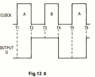
The above situation can we winessed in the Fig. 13D. Here, it looks like that the input frequency is getting divided by two.
At time T1 the clock happens to be positive-edged, therefore we don not find any switching taking place. However during time T2, we have a negative-going transition, which leads to the output suddenly changing state from low to high.
During the upcoming negative-going clock transition at time T4, the output line suddenly becomes low again.
The above procedures tells us that supplying a pair of input pulses to the clock lines (A and B) is necessary so that the output pulse is able to generate one full cycle, hence we get the following relationship:
fin = 2fout
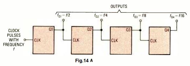
When we configure J -K flip -flops in a cascaded manner, as shown in Fig. 14A, it results in the creation of a binary-division chain. The figure exhibits a four-bit scenario, where the input clock frequency applied at the input is denoted as f, and the frequency at the Q1 input becomes f /2, at Q2 the frequency turns into f/4, at Q3 = f /8, and at Q4 it becomes f/16.
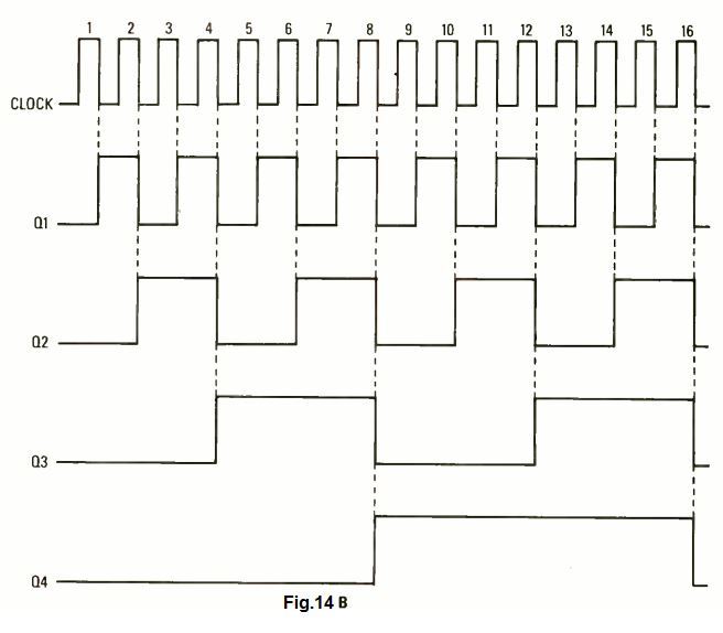
We can witness the above explained series of clock pulses and the resultant outputs in the example figure 14B.
So these were the 12 basic digital circuits typically incorporated in most advanced digital devices. If you have any further designs to add in the above list, please feel free to suggest them through the comments below.


Need Help? Please Leave a Comment! We value your input—Kindly keep it relevant to the above topic!