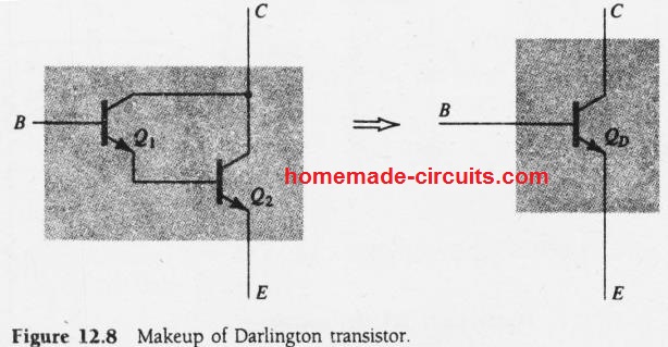
Darlington transistor is a well known and popular connection using a pair of bipolar transistor junction transistor (BJT), designed for operating like an unified "superbeta" transistor. The following diagram shows the details of the connection.
Definition
A Darlington transistor can be defined as a connection between two BJTs that allows them to form a single composite BJT acquiring a substantial amount of current gain, which may range beyond thousand typically.
The main advantage of this configuration is that the composite transistor behaves like a single device having an enhanced current gain equivalent to the product of the current gains of the each transistor.
If the Darlington connection comprises of two individual BJTs with current gains β1 and β2 the combined current gain can be calculated using the formula:
βD = β1β2 -------- (12.7)
When matched transistors are used in a Darlington connection such that β1 = β2 = β , the above formula for the current gain gets simplified as:
βD = β2 -------- (12.8)
Packaged Darlington Transistor
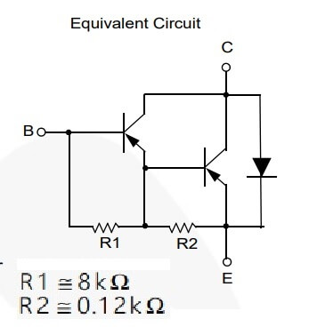
Due to its immense popularity, Darlington transistors are also manufactured and available ready made in a single package which have two BJTs internally wired up as one unit.
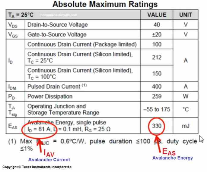
The following table provides the datasheet of an example Darlington pair within a single package.
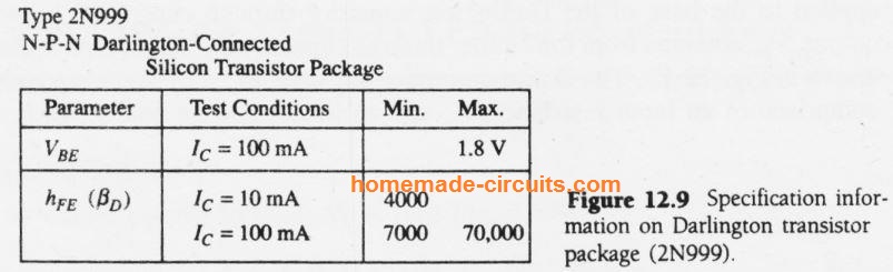
The indicated current gain, is the net gain from the two BJTs. The unit comes with 3 standard terminals externally, namely base, emitter, collector.
This kind of packaged Darlington transistors have external features similar to a normal transistor but have very high and enhanced current gain output, compared to the normal single transistors.
How to DC Bias a Darlington Transistor Circuit
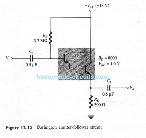
The following figure shows a common Darlington circuit using transistors with a very high current gain βD.
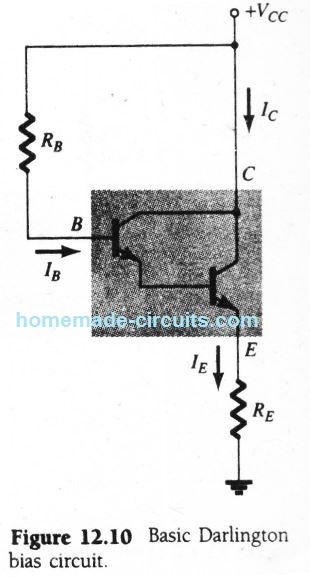
Here the base current can be calculated using the formula:
IB = VCC - VBE / RB + βDRE -------------- (12.9)
Although this may look similar to the equation which is normally applied for any regular BJT, the value βD in the above equation will be substantially higher, and the VBE will be comparatively larger. This has been also proven in the sample datasheet presented in the previous paragraph.
Therefore, the emitter current can be calculated as:
IE = (βD + 1)IB ≈ βDIB -------------- (12.10)
DC voltage will be:
VE = IE RE -------------- (12.11)
VB = VE + VBE -------------- (12.12)
Solved Example 1
From the data given in the following figure, calculate the bias currents and voltages of the Darlington circuit.
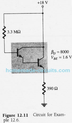
Solution: Applying Eq.12.9 the base current is determined as:
IB = 18 V - 1.6 V / 3.3 MΩ + 8000(390Ω) ≈ 2.56 μA
Applying Eq.12.10, the emitter current may be evaluated as:
IE ≈ 8000(2.56 μA) ≈ 20.28 mA ≈ IC
Emitter DC voltage can be calculated using equation 12.11, as:
VE = 20.48 mA(390Ω) ≈ 8 V,
Finally collector voltage can be assessed by applying Eq. 12.12 as given below:
VB = 8 V + 1.6 V = 9.6 V
In this example the supply voltage at the collector of the Darlington will be:
VC = 18 V
AC Equivalent Darlington Circuit
In the figure shown below, we can see a BJT emitter-follower circuit connected in Darlington mode. The base terminal of the pair is connected to an ac input signal through capacitor C1.
The output ac signal obtained through capacitor C2 is associated with the emitter terminal of the device.
The simulation result of the above configuration is presented in the following figure. Here the Darlington transistor can be seen replaced with an ac equivalent circuit having an input resistance ri and an output source of current represented as βDIb
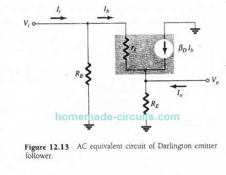
The AC Input Impedance can be calculated as I have explained below:
Ac base current passing through ri is:
Ib = Vi - Vo / ri ---------- (12.13)
Since
Vo = (Ib + βDIb)RE ---------- (12.14)
If we apply Eq 12.13 in Eq. 12.14 we get:
Ib ri = Vi - Vo = Vi - Ib (1 + βD)RE
Solving the above for Vi :
Vi = Ib[ri + (1 + βD)RE]
Vi / Ib = ri + βDRE
Now, examining the transistor base, its ac input impedance can be evaluated as:
Zi = RB ॥ ri + βDRE ---------- (12.15)
Solved Example 2
Now let's solve a practical example for the above AC equivalent emitter follower design:
Determine the input impedance of the circuit, given ri = 5 kΩ
Applying Eq.12.15 we solve the equation as given below:
Zi = 3.3 MΩ ॥ [5 kΩ + (8000)390 Ω)] = 1.6 MΩ
Practical Design
Here's a practical Darlington design by connecting a 2N3055 power transistor with a small signal BC547 transistor.
A 100K resistor is used at the signal input side to reduce the current to a few millamps.
Normally with such low current at the base, the 2N3055 alone can never illuminate a high current load such as a 12V 2 amp bulb. This is because the current gain of 2N3055 is very low to process the low base current into high collector current.
However as soon as another BJT which is a BC547 here is connected with 2N3055 in a Darlington pair, the unified current gain jumps up into a very high value, and allows the lamp to glow at full brightness.
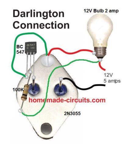
Th average current gain (hFE) of 2N3055 is around 40, while for BC547 it's 400. When the two are combined as a Darlington pair, the gain shoots up substantially to 40 x 400 = 16000, awesome isn't it. That's the sort of power we are able to get from a Darlington transistor configuration, and an ordinary looking transistor could be turned into a hugely rated device just with a simple modification.


Questions & Answers
A friend has an old Ademco alarm which has a circuit for supplying regulated 12 volts from raw 20v dc capacitor filtered full wave bridge rectified 16 v ac. It uses an old, Motorola Darlington with internal resistors. I can’t find any catalog mention of the transistor or a diagram showing what internal resistor values were used to supposedly cancel the effects of leakage. It is the JE370. (MJE 370?). Any ideas?
Yes, it seems it is nowhere mentioned in the datasheet. The following diagram is for the TIP125 transistor, which has similar features like MJE370, so possibly the internal resistor configuration for MJE370 also could be per this variant:
Hi sir i am New in the world of Electronic i have a deed darlington transistor 2sd798 and i need to make the same transistor with 2 simples bjt transistor
Sure Murad, I can help you. You can try the circuits explained in the following article:
Easy Two Transistor Projects for School Students
Build Simple Transistor Circuits
Let me know if you need any further help.
That’s the sort of power we are able to get from a Darlington transistor configuration
is it ? or we just control big current with little current ?
the power we can take is limited with the second transistors maximum current capacity i think .
Very impressive site! Was hoping I would find exactly what I am looking for and this seems to be as close as any, but not an exact match. I have a microcontroller outputting to a DAC via I2C. The DAC outputs from 0 to 4.5VDC, and that changes slightly every 125 msec. It can be driven thru the whole 4.5V range. The DAC can only source about 20 ma max. What I am looking for is a circuit stage that can provide unity voltage gain, but amplify the current capacity. This stage should have a high enough input impedance to limit the DAC current to 20 ma at a max DAC voltage output of 4.5 VDC. The output of the stage should mimic the input voltage, and be able to a 10 ohm load. So at 4.5VDC, it should be able to source 450 ma indefinitely. Looks like the a darlington pair would suffice, but I am not an electronics engineer. Any ideas would be vastly appreciated!!
Thank you! Yes a emitter follower design seems to be the best option for your specific requirement. You can certainly go ahead with it.
hi Sagatam, can you please use voltage divider biasing to establish the overall gain of Darlington pair? is always a law that the two transistors must be the same? cos I am yet to come across any rule that emphasizes that.
thanks.
Hi Abdulalim, it’s not compulsory to use matching transistors for Darlington, the gain can be easily calculated by multiplying their beta values.
Good and clear esplanation as always.
Thank you.
You are most welcome!