In this post I have explained how the internal body diodes of MOSFETs could be exploited for enabling the charging of battery through the same transformer which is being used as the inverter transformer.
In this article we will investigate a full bridge inverter concept and learn how the in-built diodes of its 4 MOSFETs could be applied for charging an attached battery.
What is a Full Bridge or H-Bridge Inverter
In few of my earlier posts we have discussed full bridge inverter circuits and regarding their working principle.
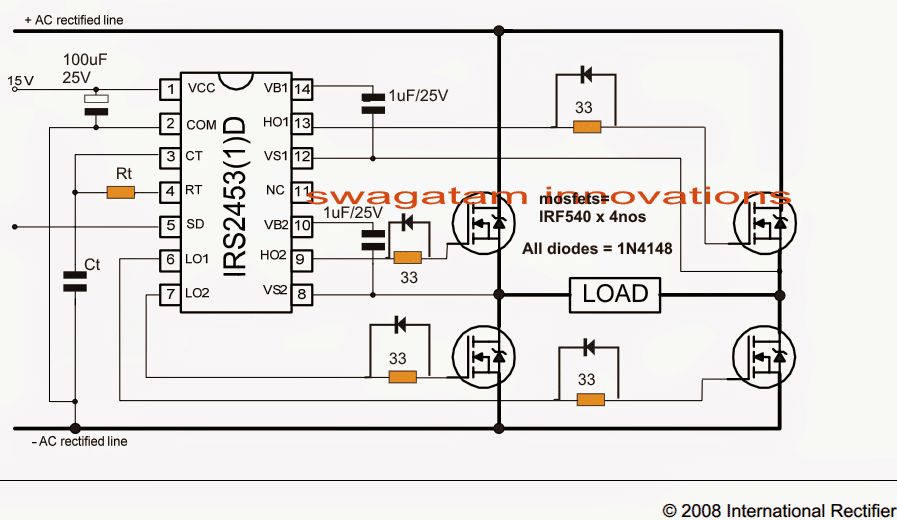
As shown in the above image, basically, in a full-bridge inverter we have a set of 4 MOSFETs connected to the output load. The diagonally connected MOSFET pairs are alternately switched through an external oscillator, causing the input DC from the battery to transform into an alternating current or AC for the load.
The load is normally in the form of a transformer, whose low voltage primary is connected with the MOSFET bridge for the intended DC to AC inversion.
Typically, the 4 N-channel MOSFET based H-bridge topology is applied in full bridge inverters, since this topology provides the most efficient working in terms of compactness to power output ratio.
Although using 4 N channel inverters depend on specialized driver ICs with bootstrapping, yet the efficiency overweighs the complexity, hence these types are popularly employed in all modern full bridge inverters.
Purpose of MOSFET Internal Body Diodes
The internal body diodes present in almost all modern day MOSFETs are primarily introduced to safeguard the device from reverse EMF spikes generated from a connected inductive load, such as a transformer, motor, solenoid etc.
When an inductive load is switched ON through the MOSFET drain, electrical energy gets stored instantaneously inside the load, and during the next moment as the MOSFET turns OFF, this stored EMF is kicked back in the reverse polarity from MOSFET source to drain, causing a permanent damage to the MOSFET.
The presence of an internal body diode across the drain/source of the device thwarts the danger by allowing this back emf spike a direct path through the diode, thus safeguarding the MOSFET from a possible breakdown.
Using MOSFET Body Diodes for Charging Inverter Battery
We know that an inverter is incomplete without a battery, and an inverter battery inevitably requires charging frequently to keep the inverter output topped-up and in the standby condition.
However, charging a battery requires a transformer, which needs to be a high wattage type to ensure optimal current for the battery.
Using a additional transformer in conjunction with the inverter transformer can be quite bulky and costly too. Therefore finding a technique in which the same inverter transformer is applied for charging the battery sounds extremely beneficial.
The presence of the internal body diodes in MOSFETs fortunately makes it possible for the transformer to be switched in the inverter mode and also in the battery charger mode, through some easy relay changeovers sequences.
Basic Working Concept
In the diagram below we can see that, each MOSFET is accompanied with an internal body diode, connected across their drain/source pins.
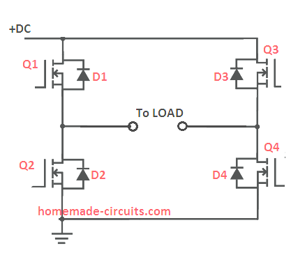
The anode of the diode is connected with the source pin, while the cathode pin is associated with the drain pin of the device. We can also see that since the MOSFETs are configured in a bridged network, the diodes also become configured in a basic full-bridge rectifier network format.
A couple of relays are employed which implement a few quick changeovers for enabling the grid AC to charge the battery via the MOSFET body diodes.
This bridge rectifier network formation of the MOSFET internal diodes actually makes the process of using a single transformer as an inverter transformer and charger transformer very straightforward.
Current Flow Direction through MOSFET Body Diodes
The following image shows the direction of current flow through the body diodes for rectifying the transformer AC to a DC charging voltage
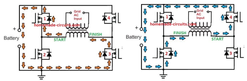
With an AC supply, the transformer wires change their polarity alternately. As shown in the left image, assuming the START as the positive wire, the orange arrows indicate the flow pattern of current via D1, battery, D3 and back to the FINISH or the negative wire of the transformer.
For the next AC cycle, the polarity reverses, and the current moves as indicated by the blue arrows via body diode D4, battery, D2, and back to the FINISH or the negative end of the transformer winding. This keeps repeating alternately, transforming both the AC cycles to DC and charging the battery.
However, since MOSFETs are also involved in the system, extreme care has to be exercised to ensure that these device do not get damaged in the process, and this calls for a perfect inverter/charger changeover operations.
Practical Design
The following diagram shows a practical design set up for implementing MOSFET body diodes as a rectifier for charging an inverter battery, with relay changeover switches.
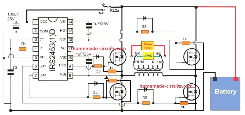
To ensure 100% safety for the MOSFETs in the charging mode and while using the body diodes with the transformer AC, the MOSFET gates must be held at the ground potential, and completely cut-off from the supply DC.
For this we implement two things, connect 1 k resistors across the gate/source pins of all the MOSFETs, and a put a cut-off relay in series with the Vcc supply line of the driver IC.
The cut-off relay is an SPDT relay contact with its N/C contacts connected in series with the driver IC supply input. In the absence of AC mains, the N/C contacts remain active allowing the battery supply to reach the driver IC for powering the MOSFETs.
When mains AC is available, this relay changes over to the N/O contacts cutting off the IC Vcc from the power source, thus ensuring a total cut off for the MOSFETs from the positive drive.
We can see another set of relay contacts connected with the transformer 220 V mains side. This winding constitutes the output 220V side of the inverter. The winding ends are connected with the poles of a DPDT relay, whose N/O an N/C contacts are configured with the mains grid input AC and the load respectively.
In the absence of mains grid AC, the system works in the inverter mode, and the power output is delivered to the load via the N/C contacts of the DPDT.
In the presence of an AC grid input, the relay activates to N/O contacts allowing the grid AC to power the 220V side of the transformer. This in turn energizes the inverter side of the transformer and the current is allowed to pass through the body diodes of the MOSFETs for charging the attached battery.
Before the DPDT relay is able to activate, the SPDT relay is supposed to cut off the Vcc of the driver IC from the supply. This slight delay in activation between the SPDT relay and the DPDT relay must be ensured in order to guarantee 100% safety for the MOSFETs and for the sound operations of the inverter/charging mode via the body diodes.
Relay Changeover Operations
As suggested above, when mains supply is available the Vcc side SPDT relay contact should activate a few milliseconds before the the DPDT relay, at the transformer side. However, when the mains input fails, both the relays must switch OFF almost simultaneously. These conditions could be implemented using the following circuit.
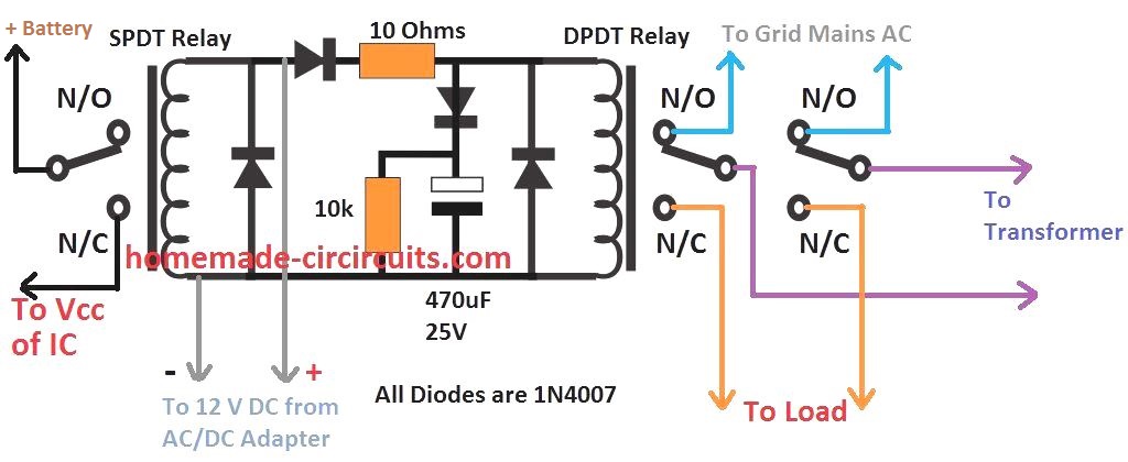
Here, the operational DC supply for the relay coil is acquired from a standard AC to DC adapter, plugged with the grid mains.
This means, when grid AC is available, the AC/DC adapter powers ON the relays. The SPDT relay being connected directly to the DC supply activates quickly before the DPDT relay can. The DPDT relay activates a few milliseconds later due to the presence of the 10 ohm and the 470 uF capacitor. This ensures that the MOSFET driver IC is disabled before the transformer is able to respond to the grid AC input at its 220 V side.
When mains AC fails, both the relay switch OFF almost simultaneously, since the 470uF capacitor now has no effect on the DPDT due to the series reverse biased diode.
This concludes our explanation regarding using MOSFET body diodes for charging an inverter battery through a single common transformer. Hopefully, the idea will allow the many hobbyists to build cheap, compact automatic inverters with built-in battery chargers, using a single common transformer.



Questions & Answers
hi… swagatam , I have once contributed about this mosfet body diode inverter circuit.here are the research I did about it which give clear explanation on bi-directional inverter with voltage boosting and current regulations when charging and inverting.
my request here is to ask you if you can create an article with schematics for it.
this are the research documentary should I post it here or via your email what’s your email if u decide?
Thank you David,
However I will need a schematic for updating the information. Without a schematic it will be difficult for me to create the article.
If you have done the experiment yourself then please provide the images of the prototype, if possible I will try to figure out the diagram…
okay, I can draw the circuit related to block diagram but I want you to go through the research I did which can will still make it easy and understanding with that you can create a schematics with reference to the research on chatgpt
I understand your desire to learn more on this subject, however I cannot use chatgpt information to publish on this site, because Google does not like AI based research, Google always prefers practical research based on real human analysis.
okay then, I will try to sketch out the schematics diagram for you to see it.
That would be great, let me know when it is ready with you….thanks very much for your kind efforts.
Very interesting post… My experience working with inverters (mostly modified sine) has built in chargers and they usually use a triac when the public grid is present. They switch through a CH relay (sometimes use DTDP relays to do this task and transfer), botton line is that triac is controlling a “Chargin tap” in the transforner normally 90VAC tap (fed with 120AC) on a 120AC transformer (double for 220VAC) which increase the charging voltage at Mostef Side. Microcontroller takes care of the 3 stages charging profiles. My question is that I’m building a sine wave inverter with 3 stages charger, the controller is meant to work 12,24,36 and 48vdc depending of some jumpers. I’m using the traditional Triac on charging Tap in the Hivoltage side of the transformer . But my Power board (6KW) it has the snubber circuit and polarizing circuit (resistor and diode) and a 20kohm resistor across gate/source instead the 1kohm as you stated . This 20k resistor will work for the same task of charging (full bridge config is used by this sinewave inverter). Thanks in advance
Hi, thanks for the feedback, and glad you liked the post.
The resistor values across the gate/source of the MOSFFETs is not critical, so a 20k resistor should also be fine. It is simply because MOSFET gates have extremely high impedance in many Megaohms, therefore a 20k will be sufficient enough to hold the gates to the ground level while they are switched OFF.
Perfect. Thanks for your kind reply.
You are welcome…
Chinonso you cannot increase your output current when charging because input mains is low all you have to do is to design a switching stabilizing unit using a ferosonite system for your inverter mains input