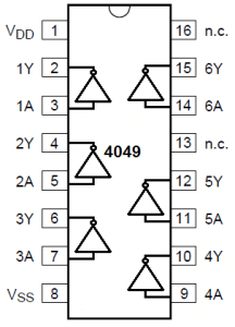
The IC 4049 is a hex inverter chip, meaning it contains six independent NOT gates inside a single 16-pin package. In this inverter design, every single gate is put to work so none of them are left floating or wasted, which prevents erratic behavior or unwanted current draw.
How it Works
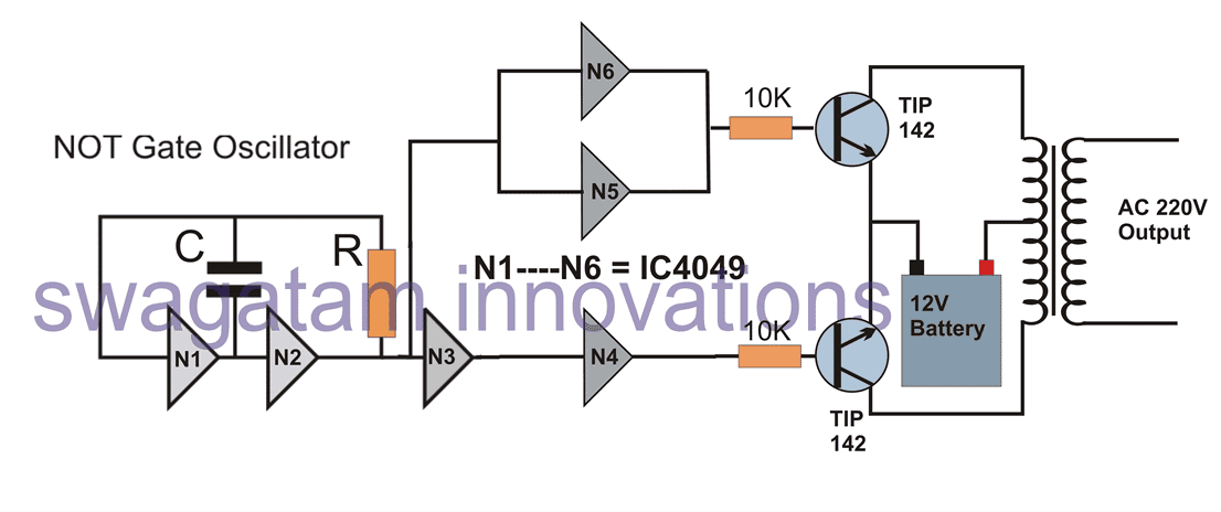
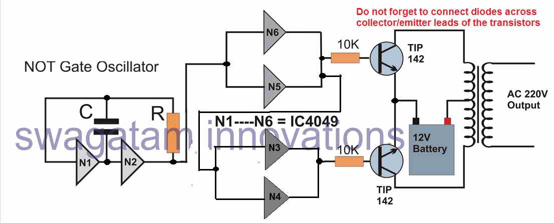
Gates N1 and N2 are wired together with an external resistor and capacitor to form an astable multivibrator oscillator. This section generates the base timing pulses at either 50 Hz or 60 Hz depending on your regional power grid requirements.
The remaining four gates, N3 through N6, are chained together in series to act as buffers and inverters. This buffering stage strengthens the weak oscillator signal and splits it into two alternating, out-of-phase square wave signals.
These alternating pulses are then fed into the power transistors or MOSFETs, forcing them to switch back and forth.
Detailed Explanation
In this simple inverter circuit we use a single IC 4049 which includes 6 NOT gates or 6 inverters inside. In the diagram above N1----N6 signify the 6 gates which are configured as oscillator and buffer stages. The NOT gates N1 and N2 are basically used for the oscillator stage, the C and R can be selected and fixed for determining the 50Hz or 60 Hz frequency as per country specs
The remaining gates N3 to N6 are adjusted and configured as buffers and inverters so that the ultimate output results in producing alternating switching pulses for the power transistors. The configuration also ensures that no gates are left unused and idle, which may otherwise require their inputs to be terminated separately across a supply line.
The transformer and battery may be selected as per the power requirement or the load wattage specifications.
The output will be purely a square wave output.
Formula for calculating frequency is given as:
f = 1 /1.2RC,
where R will be in Ohms and F in Farads
USING IC 4093 (QUAD SCHMITT TRIGGER NAND)
How it Works
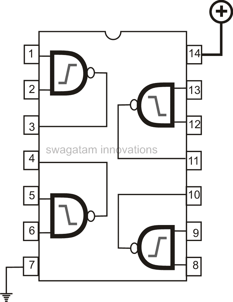
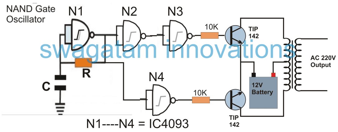
Quite similar to the previous NOT gate inveter, the NAND gate based simple inverter shown above can be built using a single 4093 IC. The gates N1 to N4 signify the 4 gates inside the IC 4093.
N1, is wired as an oscillator circuit, for generating the required 50 or 60Hz pulses. These are appropriately inverted and buffered using the remaining gates N2, N3, N4 in order to finally deliver the alternately switching frequency across the bases of the power BJTs, which in turn switch the power transformer at the supplied rate for generating the required 220V or 120V AC at the output.
Although any NAND gate IC would work here, using the IC 4093 is recommended since it features Schmidt trigger facility, which ensures a slight lag in switching and helps creating a kind of dead-time across the switching outputs, making sure that the power devices are never switched ON together even for a fraction of a second.
Detailed Circuit Analysis
The IC 4093 is a quad 2-input NAND gate chip where each gate features built-in Schmitt trigger inputs. This specific characteristic makes the IC 4093 extremely popular for simple inverter designs.
Gate N1 is configured as an oscillator to produce the required 50 Hz or 60 Hz switching frequency. Gates N2, N3, and N4 are used as buffers and inverters to drive the output stages. The main advantage of using a Schmitt trigger IC here is hysteresis. Hysteresis creates a slight, controlled delay and sharpens the edges of the square wave pulses.
This natural delay introduces a brief "dead-time" during transitions, ensuring that both opposing power transistors or MOSFETs are never switched on at the exact same moment. This prevents dangerous short-circuits (shoot-through currents) that can instantly fry your power semiconductors.
SIMPLE NAND GATE INVERTER USING MOSFETS (IC 4011 + IRF540)
Another simple yet powerful inverter circuit design is explained in the following paragraphs which can be built by any electronic enthusiast and used for powering most of the household electrical appliances (resistive and SMPS loads).
The use of a couple of mosfets influences a powerful response from the circuit involving very few components, however the square wave configuration does limit the unit from quite a few useful applications.
Introduction
Calculating MOSFET parameters may seem to involve a few difficult steps, however by following the standard design enforcing these wonderful devices into action is definitely easy.
When we talk about inverter circuits involving power outputs, MOSFETs imperatively become a part of the design and also the main component of the configuration, especially at the driving output ends of the circuit.
Inverter circuits being the favorites with these devices, we would be discussing one such design incorporating MOSFETs for powering the output stage of the circuit.
Referring to the diagram, we see a very basic inverter design involving a square wave oscillator stage, a buffer stage and the power output stage.
The use of a single IC for generating the required square waves and for buffering the pulses particularly makes the design easy to make, especially for the new electronic enthusiast.
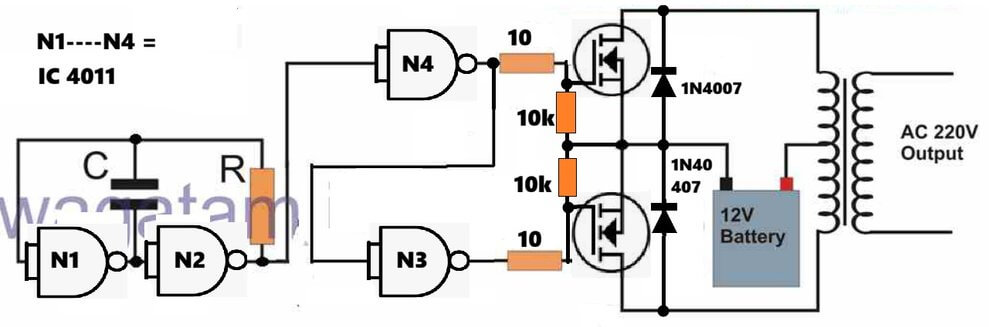
This circuit is another very popular and simple way to build a small power inverter using a quad NAND gate chip called the IC 4011. Just like the IC 4093 version, it takes 12 volt direct current from a battery and turns it into alternating current to run household appliances.
HOW THE OSCILLATOR WORKS
The first two NAND gates, labeled N1 and N2, are hooked up together with a resistor (R) and a capacitor (C) to act as an electronic pulse maker or oscillator. This part creates the steady back-and-forth ticking or frequency needed for the inverter, which is usually set to 50 Hz or 60 Hz.
THE BUFFER AND MOSFET SWITCHING STAGE
The remaining two gates, N3 and N4, take the pulses from the oscillator and split them into two opposite signals. These signals pass through small 10 ohm resistors and trigger the gates of two power MOSFETs. The 10k resistors placed between the gate and source help drain the charge quickly so the MOSFETs turn off cleanly.
The two MOSFETs act as heavy duty electronic switches that pull the 12 volt battery current alternately through the halves of the transformer's primary winding.
PROTECTION DIODES AND TRANSFORMER OUTPUT
You will also notice 1N4007 diodes connected across the MOSFETs. These are flyback or catch diodes that protect the transistors from dangerous voltage spikes when the transformer's magnetic field collapses.
Finally, the center-tapped transformer takes this rapid switching action and steps the low battery voltage up to a high 220 volts AC on the secondary output side.
Parts List for the above explained 150 watt inverter circuit diagram:
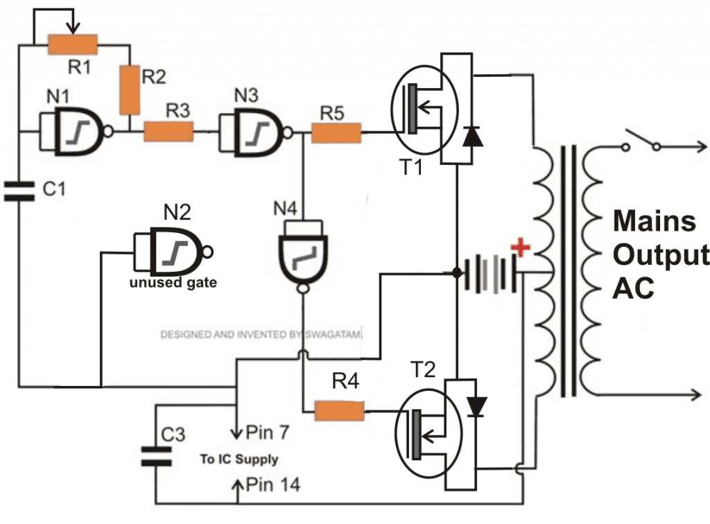
- R1 = 220K pot, needs to be set for acquiring the desired frequency output.
- R2, R3, R4, R5 = 1K,
- T1, T2 = IRF540
- N1—N4 = IC 4011
- C1 = 0.01uF,
- C3 = 0.1uF
TR1 = 0-12V input winding, current = 15 Amp, output voltage as per the required specs
Formula for calculating frequency will be identical to the one described above for IC 4049.
f = 1 /1.2RC. where R = R1 set value, and C = C1
6) Using IC 4060
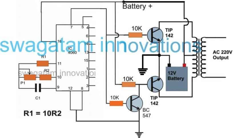
If you have a single 4060 IC in your electronic junk box, along with a transformer and a few power transistors, you are probably all set to create your simple power inverter circuit using these components. The basic design of the proposed IC 4060 based inverter circuit can be visualized in the above diagram. The concept is basically the same, we use the IC 4060 as an oscillator, and set its output to create alternately switching ON OFF pulses through an inverter BC547 transistors stage.
Just like IC 4047, the IC 4060 requires an external RC components for setting up its output frequency, however, the output from the IC 4060 are terminated into 10 individual pinouts in a specific order wherein the output generate frequency at a rate twice that of its preceding pinout.
Although you may find 10 separate outputs with a rate of 2X frequency rate across the IC output pinouts, we have selected the pin#7 since it delivers the fastest frequency rate among the rest and therefore may fulfil this using standard components for the RC network, which may be easily available to you no matter in which part of the globe you are situated in.
For calculating the RC values for R2 +P1 and C1 and the frequency you can use the formula as described below:
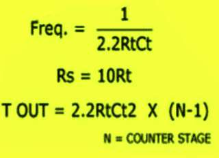
Or another way is through the following formula:
f(osc) = 1 / 2.3 x Rt x Ct
Rt is in Ohms, Ct in Farads
More info can be obtained from this article


Need Help? Please Leave a Comment! We value your input—Kindly keep it relevant to the above topic!